Photoluminescence (PL) is a classical contact-less and well-established tool for semiconductor characterization [
1]. It is, thus, highly applicable to the direct band gap semiconductor gallium nitride (GaN) and its relatives, all of which are well-known for their high PL quantum efficiency. Although the required technical components have already been available for many years, the quasi-continuous PL scanning of GaN and InGaN epitaxial layers at high temperatures—typically at 700 °C or even higher if, e.g., metal organic chemical vapor deposition (MOCVD) is considered—was, however, developed and reported quite recently [
2,
3,
4]. We have already demonstrated that reasonably strong PL spectra from GaN and InGaN layers were obtained during growth in a quasi-commercial MOCVD reactor at temperatures around 1050 °C for GaN and 730 °C for InGaN, which provided a useful correlation with the composition of the deposited In
xGa
1−xN layers, permitting MOCVD process optimization at the earliest possible stage. This is interesting because device optimization in the sense of targeting, e.g., a particular emission wavelength, as well as a better yield for the designated light emitting diode (LED) structure is now accessible within such an in situ PL technique. The in situ PL signal also carries other information from the epitaxial layer growth [
2,
3], e.g., it correlates with the layer thickness and, hence, with the growth rate (while exploring the interference pattern in the PL spectra), with the layer temperature (via redshift, broadening, and attenuation of the PL with increasing temperature), with the interface roughness (while analyzing, e.g., the modulation depth of the interference pattern in the PL spectrum), and with the (self-) absorption coefficient (given by the attenuation of the PL interference pattern toward shorter wavelengths). Interestingly, we observed in our various in situ high-temperature PL measurements [
2,
3,
4] that the general PL behavior at high temperatures was quite similar [
4] (regardless of a potential difference in peak wavelengths) for a bulk GaN substrate layer and a multi-quantum well (MQW) InGaN structure for LED devices. Therefore, our considerations apply for both the bulk GaN and also for the more complex InGaN structures, rendering such a high-temperature PL characterization/monitoring scheme quite general.
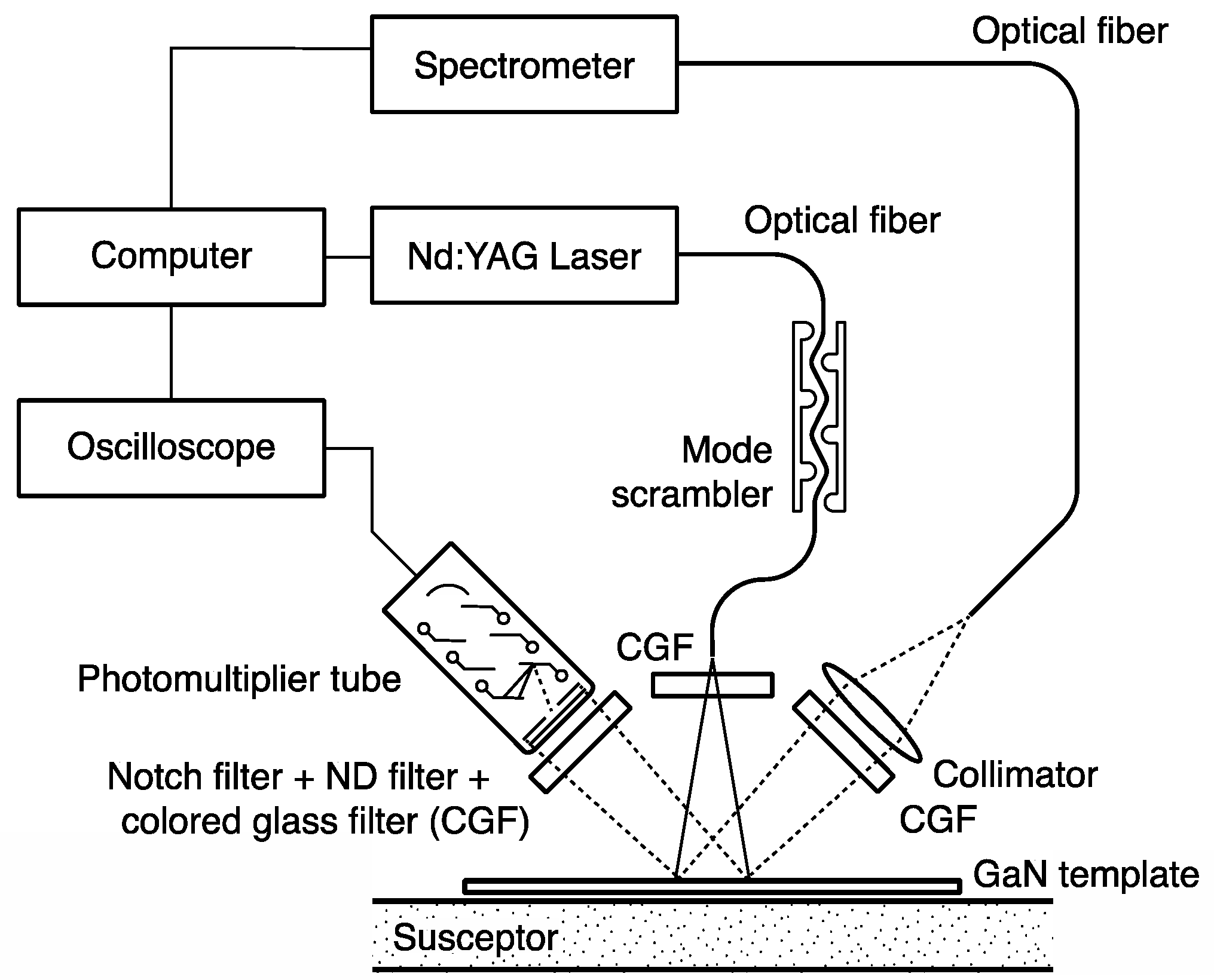
In an MOCVD growth process high UV excitation densities are needed to obtain reasonable PL signals at high temperatures [
2,
3,
4]. The excitation is provided by a repetitive (up to 20 Hz) pulsed near-UV laser with a high peak power density (in the order of MW/cm
2) providing short pulses in the order of ns, with approximately 1–10 mW average power. As previously shown, a repetitive pulsed excitation (a) promotes sufficient PL at high temperatures and (b) neither damages the material nor interferes with the epitaxial growth [
3]. In contrast, a continuous UV laser with equivalent power emission (e.g., 10 mW, continuous wave, CW) is hardly capable to excite reasonably efficient PL at those high temperatures. Even when increasing the CW laser power and power density by focusing the beam to small spot sizes, the PL signal remains poor, whereas the semiconductor material gets damaged, or even fully destroyed, by the intense CW laser spot.
The obtained PL spectra regularly contain interference fringes, which could be analyzed for a thickness or growth rate determination. Similar—but not identical—interference measurements with external light sources are already well established in thin film monitoring. However, there are subtle differences between thin film interference fringes from external illumination and from an internal PL process. These differences are frequently missed in the scientific discourse of PL spectra from thin films. This contribution describes and models these two different and photonic effects in thin films. For better clarity, the photonic effects are presented and discussed separately from the electronic transitions.
1.1. Considerations for Characteristic Electronic Transitions in High-Temperature PL
Referring to the above mentioned and superlinear excitation mechanisms [
2,
3,
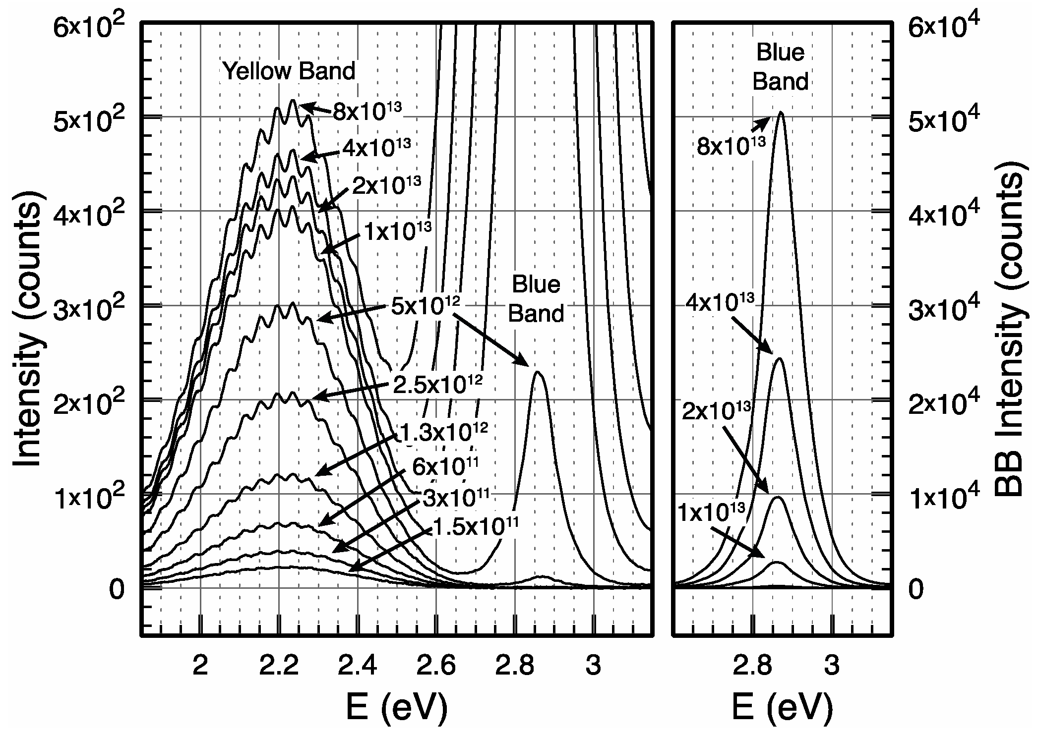
4] it is to note that a similar non-linearity in the GaN material or InGaN MQW material is already present at room temperature and can be readily visualized using, e.g., a sapphire wafer coated with GaN/InGaN MQW layers (representing the standard material system for LEDs) illuminated by a conventional UV fluorescence lamp (i.e., a “black light” at 350–400 nm) with a low irradiation density in the order of 10
1–10
2 µW/cm². At these low excitation densities, the LED wafer will not emit the characteristic emission wavelengths of the LED (e.g., blue light around 450 nm). Instead, a rather effective and pale-yellowish fluorescence (centered at approximately 570 nm, 2.2 eV) is observed, which is readily visible to the naked eye. This yellowish emission, which we term as the “yellow band” (YB) is attributed to defects in the GaN lattice [
5,
6].
When increasing the excitation density on the wafer, e.g., by using a CW HeCd pump laser beam at 325 nm with some mW/mm2 or with an ordinary electronic injection current of several mA/mm² through the LED chip, the designated wavelength, namely, the blue light at 450 nm, clearly dominates the PL emission. This is the expected emission associated to the InGaN band gap and herein denoted as the “blue band” (BB); however, it certainly also covers the near-UV wavelength range for GaN at room temperature.
Both the YB and BB emissions emerge from competing relaxation processes, and the interplay between these processes is found to be similar for simple GaN or complex InGaN MQW [
4].
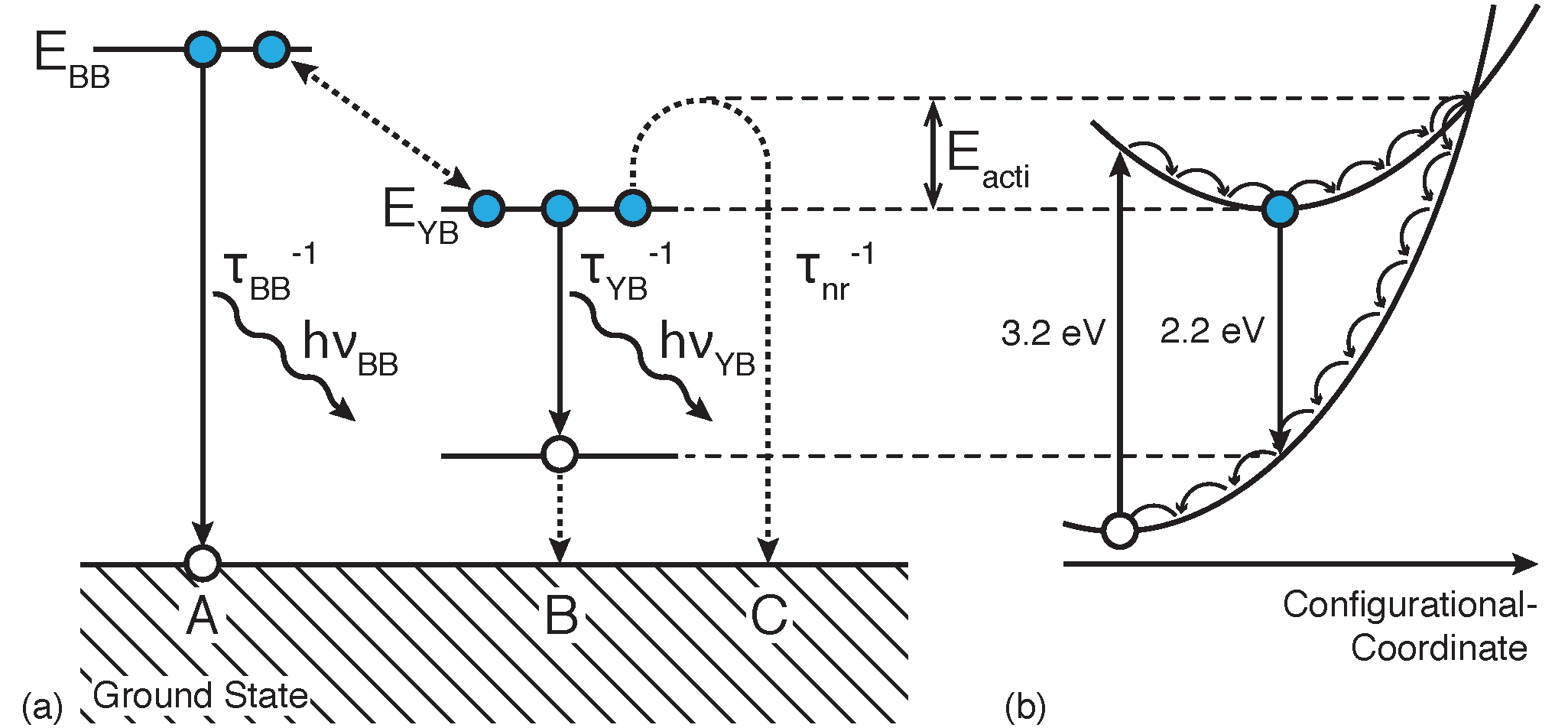
A non-equilibrium carrier in a BB state can relax into a vacant YB state (
Figure 1) and, subsequently, emit a yellowish light at the expense of the BB emission. Since both the YB defect density and the defects’ individual recombination rates at room temperature are limited, the YB provides a quenching process for the BB that is easily saturated [
5] (e.g., in a conventional LED at few mA injection current). Thus, above certain excitation thresholds, the BB gains intensity and will clearly dominate the PL emission at room temperature; however, the saturated YB is still present with considerably weaker relative intensities (as later shown in
Section 3.1). The competition between BB and YB is experimentally observable in GaN bulk material and also—very similar—in more complex InGaN MQW samples, as shown later in
Section 3.1. As very common in luminescence, a transfer from BB inside an InGaN quantum well to YB even outside of the quantum well (GaN) can readily occur via energy transfer, an actual escape of carriers from the QW is not required for this process. Energy transfer over a distance of several nm between two insulated luminescence centers (=high potential barrier between them) is a common, efficient, and fast process, such as non-radiative near-field dipole-dipole interactions, like Förster resonance energy transfer (FRET). The energies, but not the particles are transferred. In the resonance case (the emission level fits the absorption level), the transfer can quickly occur over several nm and energy transfer readily passes potential barriers. This explains the similar behavior of GaN and InGaN MQW.
As a conjecture of this research, the YB defects not only convert the excitation energy into an emission of yellowish light with a comparably slow and saturable recombination process [
5,
8], but such defects (or those which closely interact) also establish an additional parallel recombination channel, which is thermally activated and non-radiative. At room temperature, this non-radiative recombination is slow and not very effective. Hence, the luminescence efficiency of high quality GaN samples reaches rather high internal quantum yields virtually at 100% [
9,
10,
11]. However, at higher temperatures, the non-radiative recombination process drastically accelerates and efficiently overtakes—i.e., quenches—both the YB and BB emissions rendering the overall PL to be affected at higher temperatures.
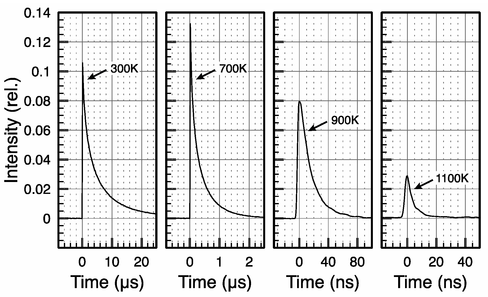
Nevertheless, when providing UV excitation at a higher rate (i.e., at higher power densities) that exceeds the thermally-quenching process, reasonably intensive BB and YB emissions are possible. The thermally-activated fast non-radiative recombination pathway over a limited number of defects is finally limited and can, therefore, be saturated with sufficient excitation power. As experimentally observed, this single mechanism turned out to be well-suited to describe the non-linear PL phenomena at high temperatures. The nonlinear behavior, as described here, may promote the irreplaceability of high (peak) power density UV excitation when sufficient PL emission at high temperatures is needed, e.g., for monitoring the growth of InGaN quantum wells inside a quasi-industrial MOCVD system via PL emission [
2,
3]. At room temperature (and above) only the near band gap BB and the broad YB emissions are visible. Other, more detailed, spectral features associated with, e.g., excitons or defined defect levels [
5], are merely present at low temperatures, rendering them either blurred or dark at high temperatures, or even unobservable.
Since the prominent YB defects, together with closely-interacting dark defect states, are conjectured to play a governing role as a temperature-activated quenching path [
7], their nature must be discussed in more detail. Although the YB luminescence and associated defects have been extensively studied, a detailed prescription towards an efficient PL at high temperatures is still lacking. In the following, the characteristic features of YB defects are briefly outlined along with the comprehensive review by Reshchikov et al. [
5].
A considerable number of rather different, but mostly point-like, defects are associated with the YB-PL, such as Ga vacancies, complexes, and intentional or unintentional impurities [
5]. For investigating the nature of the YB, 35 elements were implanted in GaN and most of them appear to increase the YB luminescence [
5,
12]. Additional experiments and calculations support the theory of gallium vacancies or impurities (such as carbon) are responsible for the YB [
5,
6]. The diversity of such luminescent defects in GaN and their possible transitions are considerably high. Therefore, it is remarkable that the collective behavior of all of these different defects can be represented just by one effective defect around the YB level modeled with rather few parameters, such as a single defect density and the relevant transition channels. With its broadband emission at around 2.2 eV, the apparent significant Stokes shift at excitation energies >3 eV and the temperature-independent peak emission wavelength [
1,
5], this defect can be associated with a typical luminescence center with strong electron-lattice coupling, whose configuration coordinate (CC) model is illustrated in
Figure 1b [
1,
5,
7]. Furthermore, the effective YB defect must be considered as an acceptor because the luminescent GaN layers are typically n-conducting, with free electron densities of approximately 10
18 cm
−3 at room temperature [
13]. Therefore, the relevant non-equilibrium carriers are usually holes, and these interact with, more or less, deep acceptor levels above the valence band. The ground state of the YB acceptor in
Figure 1a was achieved by a complete filling of the defect with electrons. In the ground state, the acceptor can capture a hole, which in
n-GaN can be generated by a UV photon, from the valence band.
Alternatively, a UV excitation at around 3.2 eV [
5] can directly lift an electron from the acceptor to the conduction band, or to suitable donor levels, leaving a hole behind. The bound hole in the acceptor represents the excited state of the YB defect. The excited state quickly relaxes via multiphonon emissions (as indicated in
Figure 1b by the cascaded relaxation process) to a minimum, i.e., to a somewhat shifted coordinate of the underlying nucleus. The more the apparent shift of the coordinate of the excited state with respect to the ground state, the stronger the electron-lattice coupling of the system, which is characterized by the Huang-Rhys factor [
1,
5]. This factor is approximately 6.5 for the YB defect [
14], which indicates a strong electron-lattice coupling. For this reason, only approximately 2.2 eV is available for the photon emission at the typical YB center wavelength, however, for an excitation energy of 3.2 eV. The excess energy is thermalized by multiple phonon emissions. The strong Stokes shift results in negligible self-absorption of the emitted light. In contrast, the short-wavelength wing of the BB luminescence usually undergoes notable self-absorption in either the GaN or InGaN material system. The YB transition back to a ground state occurs via capturing a free or bound electron (from a donor level) followed by photon emission and the elimination of the bound hole while restoring the ground state of the defect.
It should be noted that, for a luminescent center with strong electron-lattice coupling and, thus, with a significant coordinate offset between both dispersion parabolas in the schematic CC diagram (cf.
Figure 1b), a crossover point between the excited and the ground exists at a certain energy level. At elevated temperatures, the electrons in the excited state can absorb a sufficient number of phonons (i.e., thermal excitation from the environment) while approaching the crossover point from which they can thermalize to the ground state without any photon emission. This is a well-known mechanism [
1,
5,
15,
16] for a thermally-activated non-radiative recombination channel of a luminescent center with high electron-lattice coupling, which is capable of providing the aforementioned quenching of the YB and BB.
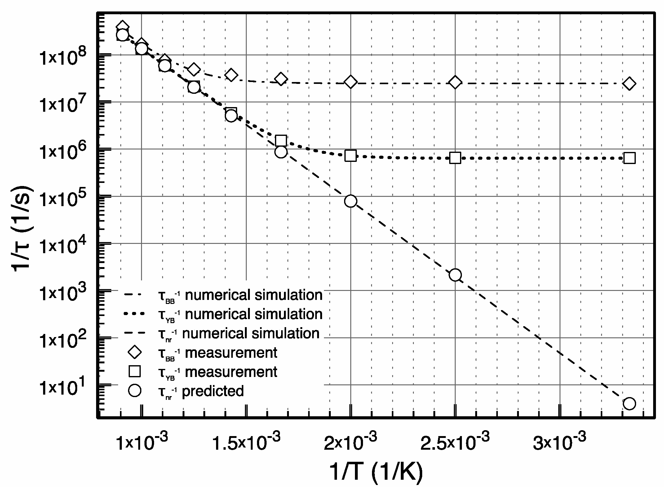
The activation energy for such temperature quenching of the YB luminescence is reported [
7] in the order of approximately 0.9 eV at low excitation densities, as well as at relatively moderate temperatures (<700 K) [
5]. However, when reaching a high excitation power at typically 20 W/cm² [
5,
15,
16], which is actually far less than applied here, a lowered activation energy of around 0.65 eV was observed in [
5,
15], which is similar to the values found in this study. It remains unclear how the proper quenching mechanism becomes effective: whether at high temperatures the YB defects, themselves, either quench the excitation or whether an energy transfer occurs towards certain other invisible defects providing a similar outcome for the temperature activated quenching. Currently, these two contributions are hardly distinguishable for the reported PL methods. However, the proposed PL model neither requires, nor involves, such additional transitions for explaining the above observations. In our model for rather high temperatures and high-quality samples (the designated application), just the broad BB and the broad YB remain. There is nothing more observable, as mentioned above and as previously shown [
2,
3,
4] in high-temperature PL spectra. Just these two bands, their individual behavior, and their interaction are modeled.
Thus, to flesh out the proposed model the aforementioned three major recombination pathways have to be considered (cf.
Figure 1b): the BB emission (transition A) with a certain rate over the material band gap, which is tapped and eventually quenched by the luminescent and saturable YB defects (transition B), where the YB defects are simultaneously depopulated by a temperature activated non-radiative relaxation process (transition C).
1.2. Considerations for Characteristic Photonic Effects in Thin Luminescent Layers
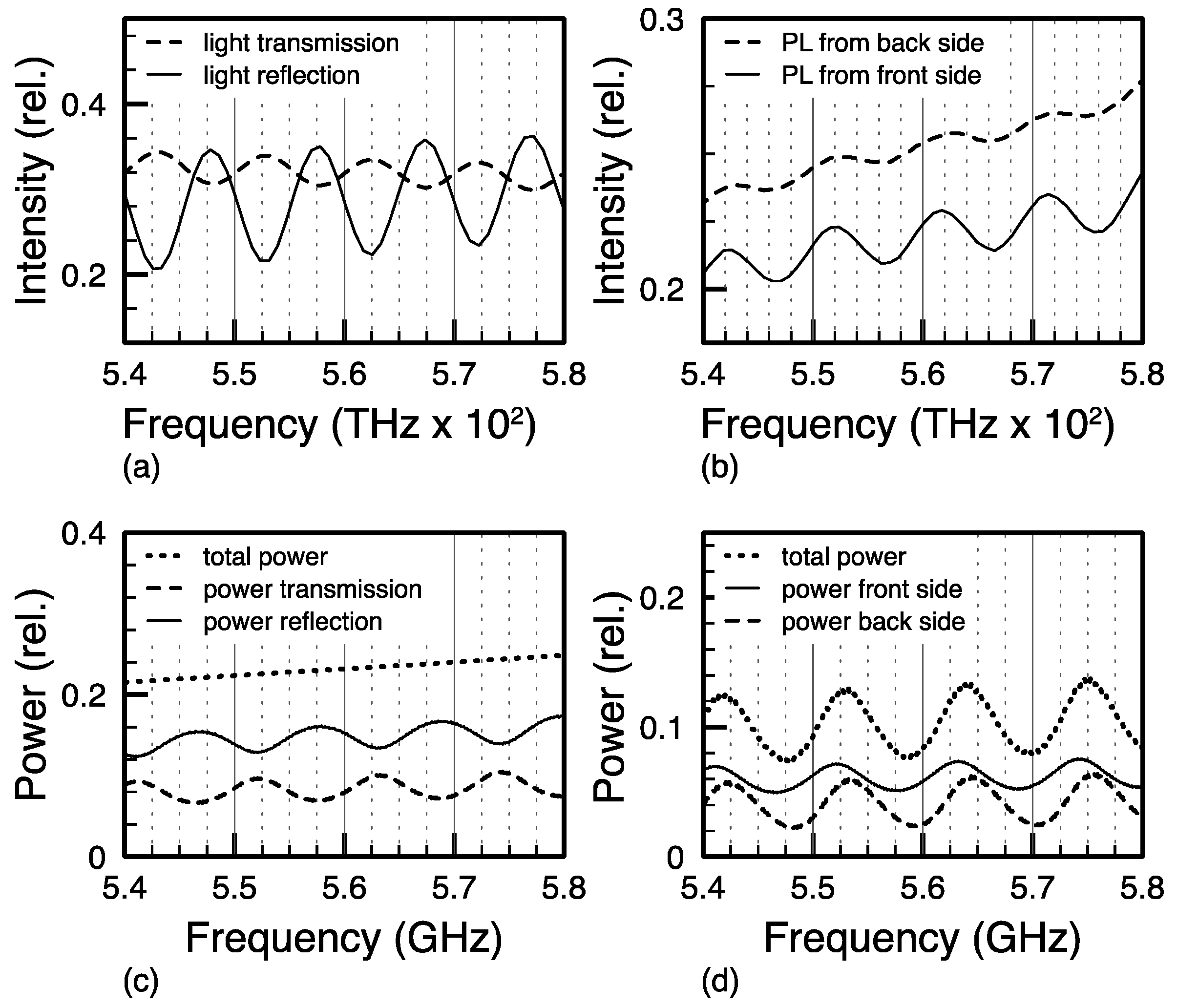
In addition to the microscopic electronic PL mechanism, macroscopic photonic effects have to be taken into account. The broadband YB emission (with strong stokes shift and virtually no self-absorption) from the thin GaN layer showed a typical and almost regularly observed modulation in the luminescence spectra (e.g.,
Section 3.1) that is commonly linked to Fabry–Pérot interference fringes. The latter can be directly assigned to the layer thickness and the index of refraction of the thin film. Interestingly, this interpretation seems to not be exactly right as the actual Fabry–Pérot oscillations (FPO) are usually retrieved from
external white light illumination of thin films, whereas the nearly-identical modulation pattern observed in the present experiment stems from the PL as an
internal light source intrinsic to the luminescent thin film.
It can be argued that a FPO cannot be held responsible for the modulation pattern of internal PL due to principal reasons: When considering a lossless optically-smooth thin film with a certain index of refraction, energy conservation is immediately applicable. Given an experiment with external white light illumination, the interference fringes of the thin film´s reflection spectra must find its exact counterparts to a 180° phase shift in the film´s transmission spectra. Both spectra, when superimposed, must reproduce the smooth spectrum of the original white light source, without any interference modulation. Such results are regularly achieved in sufficiently careful experiments. Hence, when looking at the modulation of the YB’s luminescence spectra from thin GaN films (e.g.,
Section 3.1), similar interference fringes can be observed in the PL spectra emitted from the film´s front side. Inside the film an internal white light source is active and no self-absorption of the emitted white light is assumed. However, when inspecting the back side of the thin film, the modulation pattern in the emitted PL spectra looks the same, but without a 180° phase shift. This is due to symmetry because there is no difference between the front and back of a free-standing, homogeneous thin film with a built-in light source (i.e., the PL). In the lossless case this necessarily implies that the atomic emission itself has to undergo a spectral modulation, aiming at what is known as the Purcell effect [
17,
18,
19,
20,
21]. Therefore, the Purcell effect presented here represents not only a conventional interference, but an imprint of the (macroscopic) thin film cavity on the spontaneous emission process itself.
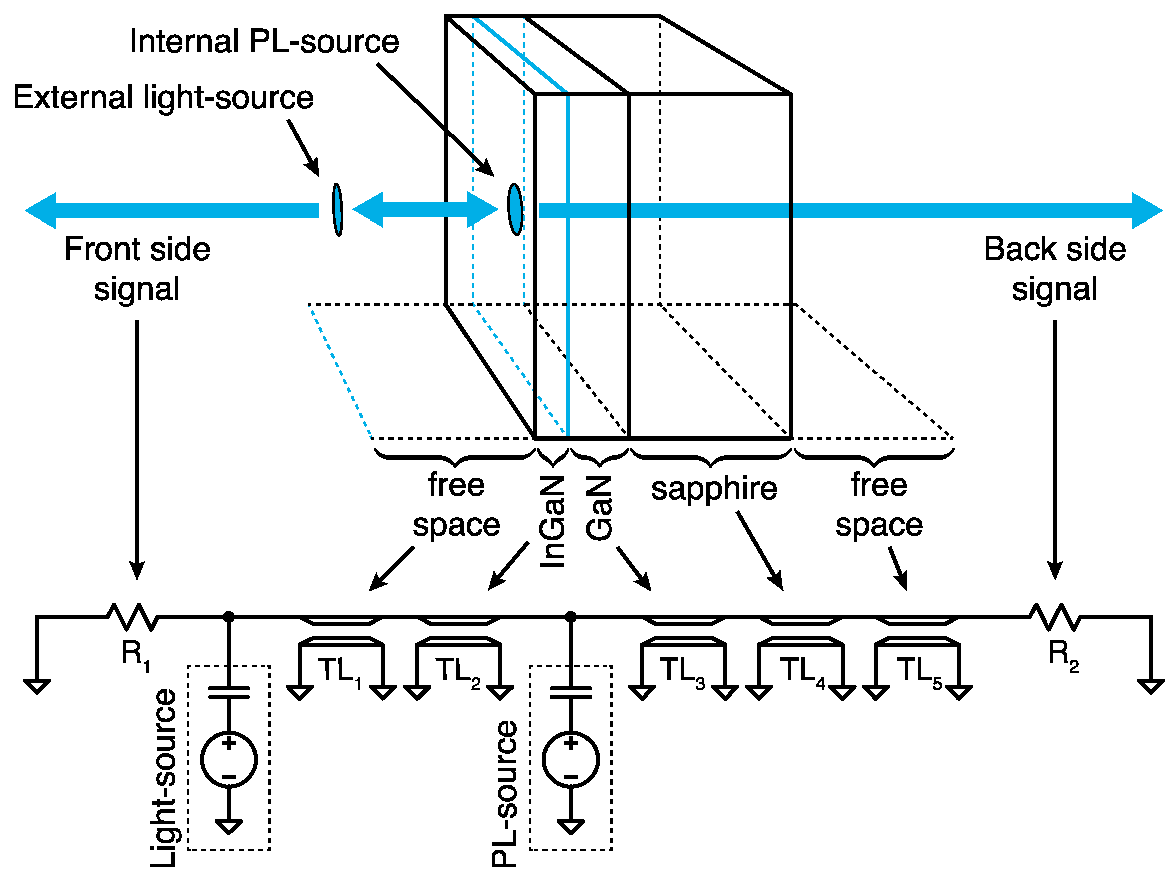
In order to scrutinize the various aforementioned contributions to the PL modulation an intuitive frequency-scaled 1D equivalent circuit model of the optically-activated one-dimensional InGaN/GaN thin-film layer system is presented (cf.
Section 2.2). The model is based on RF transmission lines mimicking the light propagation in the corresponding layers while using broadband voltage sources either placed externally (white light illumination) or internally (active luminescence) for the optical excitation of the layer system. The electrical equivalent circuit model, thus, allows a one-dimensional simulation of the spectral features of PL emission from the overall layer stack providing clarification of the observed interference/luminescence effects, even for arbitrarily complex layer structures.


