
Effect of Annealing Time of GaN Buffer Layer on Curvature and Wavelength Uniformity of Epitaxial Wafer

Abstract
1. Introduction
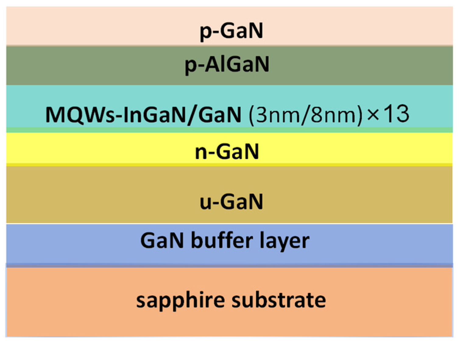
2. Experiment
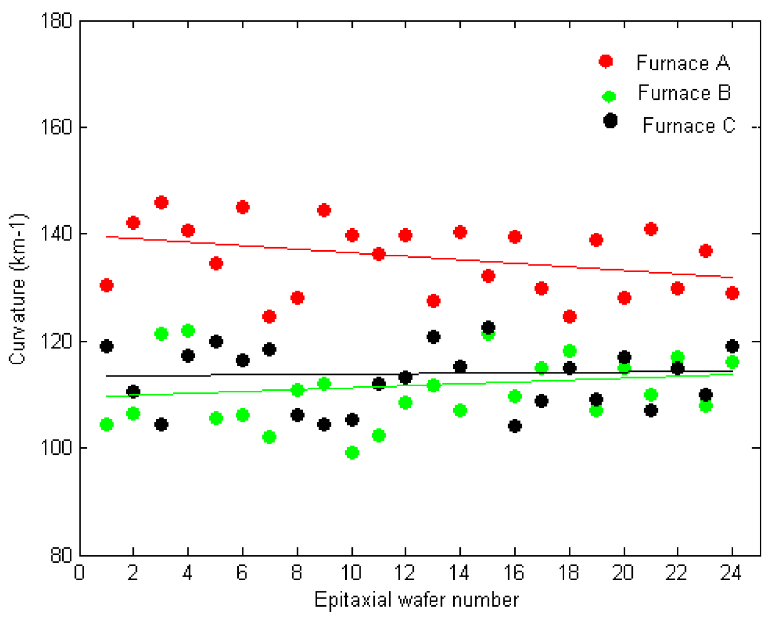
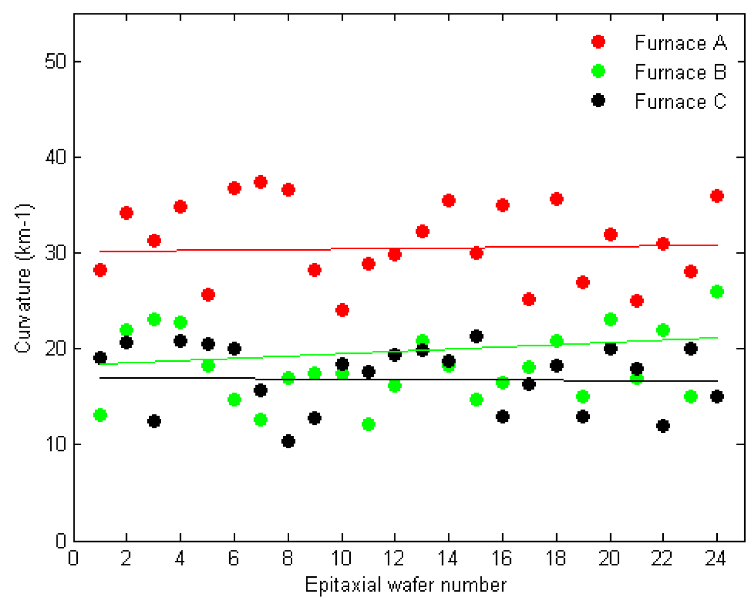
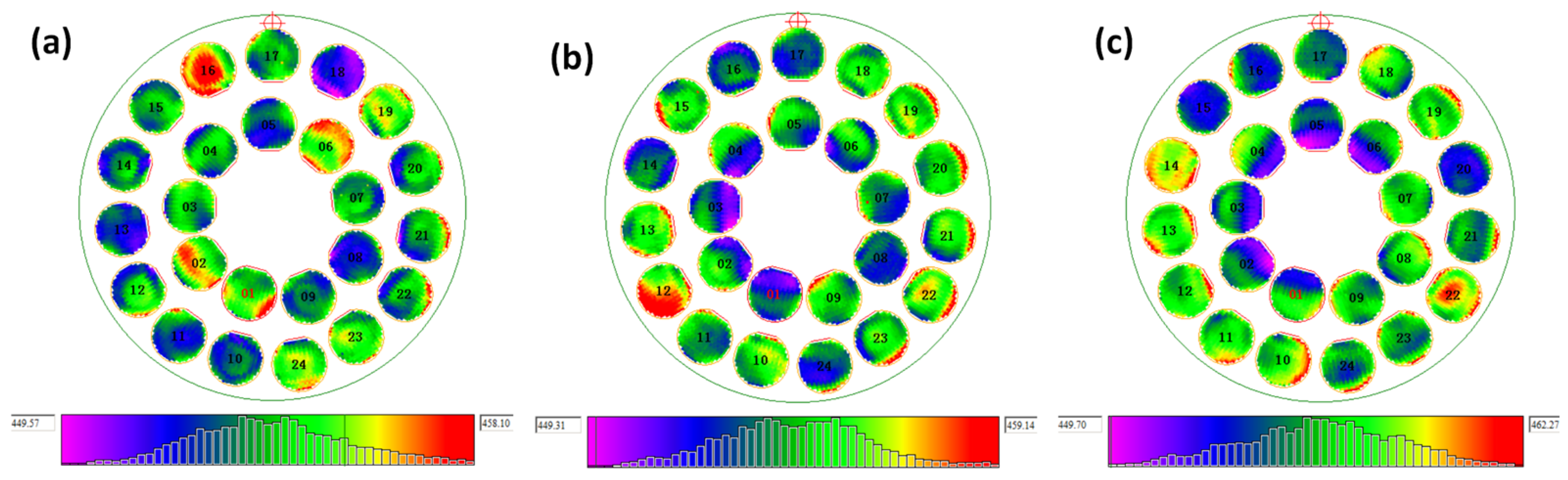
3. Results and Discussion
4. Conclusions
Author Contributions
Funding
Data Availability Statement
Conflicts of Interest
References
- Lee, J.H.; Kang, M.H.; Yi, S.C.; Park, J.H.; Oh, N. Counterbalancing effects of bowing in gallium nitride templates by epitaxial growth on pre-strained sapphire substrates. Ceram. Int. 2024, 50, 47666–47676. [Google Scholar] [CrossRef]
- Serafińczuk, J.; Moszak, K.; Pawlaczyk, Ł.; Olszewski, W.; Pucicki, D.; Kudrawiec, R.; Hommel, D. Determination of dislocation density in GaN/sapphire layers using XRD measurements carried out from the edge of the sample. J. Alloys Compd. 2020, 825, 153838. [Google Scholar] [CrossRef]
- Aida, H.; Kim, S.; Suzuki, T. Estimation of bowing in hetero-epitaxial GaN-on-sapphire substrate at elevated temperatures by X-ray diffraction rocking curve measurement. J. Cryst. Growth 2015, 412, 60–66. [Google Scholar] [CrossRef]
- Huang, C.Y.; Hagedorn, S.; Walde, S.; Tsai, C.L.; Fu, Y.K.; Weyers, M. The optimal threading dislocation density of AlN template formicrometer-thick Al0.63Ga0.37N heteroepitaxy. J. Cryst. Growth 2022, 600, 126910. [Google Scholar] [CrossRef]
- Chena, F.; Jia, X.H.; Lau, S.P. Recent progress in group III-nitride nanostructures: From materials to applications. Mat. Sci Eng. R 2020, 142, 100578. [Google Scholar] [CrossRef]
- Cui, S.Y.; Sun, K.; Liao, Z.F.; Zhou, Q.; Jin, L.; Jin, C.; Hu, J.; Wen, K.-S.; Liu, S.; Zhou, S. Flexible nanoimprint lithography enables high-throughput manufacturing of bioinspired microstructures on warped substrates for efficient III-nitride optoelectronic devices. Sci. Bull. 2024, 69, 2080–2088. [Google Scholar] [CrossRef]
- Zhou, Y.; Xu, L.; Liu, S. Optimization for warpage and residual stress due to reflow process in IGBT modules based on pre-warped substrate. Microelectron. Eng. 2015, 136, 63–70. [Google Scholar] [CrossRef]
- Liu, J.; Zhang, J.; Mao, Q.; Wu, X.; Jiang, F. Effects of AlN interlayer on growth of GaN-based LED on patterned silicon substrate. CrystEngComm 2013, 15, 3372–3376. [Google Scholar] [CrossRef]
- Xiang, R.F.; Fang, Y.Y.; Dai, J.N.; Zhang, L.; Su, C.; Wu, Z.; Yu, C.; Xiong, H.; Chen, C.; Hao, Y. High quality GaN epilayers grown on Si (111) with thin nonlinearly composition-graded AlxGa1-xN interlayers via metal-organic chemical vapor deposition. J. Alloys Compd. 2011, 509, 2227–2231. [Google Scholar] [CrossRef]
- Ma, J.B.; Zhang, Y.C.; Li, Y.F.; Zhang, T.; Yao, Y.; Feng, Q.; Bi, Z.; Zhang, J.; Hao, Y. Mechanistic influence on uniformity of sheet resistance of AlGaN/GaN HEMT grown on Si substrate with the graded AlGaN buffer layers. Vacuum 2022, 199, 110966. [Google Scholar] [CrossRef]
- Xu, C.Z.; Cai, L.; Zheng, J.J.; Lin, H.X.; Chen, Z.C.; Niu, K.; Cheng, Z.J.; Xiong, F.B. The effect of different AlGaN insertion layer thicknesses on the photoelectric properties of InGaN/AlGaN near UV light emitting diodes. Results Phys. 2023, 55, 107111. [Google Scholar] [CrossRef]
- Wang, W.; Gan, X.W.; Xu, Y.; Wang, T.; Wu, H.; Liu, C. High-quality n-type aluminum gallium nitride thin films grown by interrupted deposition and in-situ thermal annealing. Mat. Sci. Semicon. Proc. 2015, 30, 612–617. [Google Scholar] [CrossRef]
- Wang, M.T.; Brunner, F.; Liao, K.Y.; Li, Y.L.; Tseng, S.H.; Weyers, M. Optimization of GaN wafer bow grown on cone shaped patterned sapphire substrates. J. Cryst. Growth 2013, 363, 109–112. [Google Scholar] [CrossRef]
- Zhe, L.; Wang, X.; Wang, J.; Hu, G.; Guo, L.; Li, J.; Li, J.; Zeng, Y. Effects of buffer layers on the stress and morphology of GaN epilayer grown on Si substrate by MOCVD. J. Cryst. Growth 2007, 298, 281–283. [Google Scholar]
- Ryu, J.H.; Chandramohan, S.; Kim, H.Y.; Kang, J.H.; Hong, C.-H.; Cho, H.K.; Song, H.D.; Kwon, H.-K. Minimization of wafer bowing in GaN-based vertical light-emitting diodes by selective area growth using metal-organic chemical vapor deposition. J. Cryst. Growth 2011, 314, 66–70. [Google Scholar] [CrossRef]
- Kozawa, T.; Kachi, T.; Kano, H.; Nagase, H.; Koide, N.; Manabe, K. Thermal strain in GaN epitaxial layers grown on sapphire substrates. J. Appl. Phys. 1995, 77, 4389. [Google Scholar] [CrossRef]
- Nakamura, S. The Roles of Structural Imperfections in InGaN-Based Blue Light-Emitting Diodes and Laser Diodes. Science 1998, 281, 956–961. [Google Scholar] [CrossRef]
- Lim, S.H.; Dolmanan, S.B.; Tong, S.W.; Liu, H.F. Temperature dependent lattice expansions of epitaxial GaN-on-Si heterostructures characterized by in- and ex-situ X-ray diffraction. J. Alloys Compd. 2021, 868, 159181. [Google Scholar] [CrossRef]
- Yao, Y.Z.; Sato, K.; Sugawara, Y.; Okada, N.; Tadatomo, K.; Sasaki, K.; Kuramata, A.; Ishikawa, Y. Three-dimensional curving of crystal planes in wide bandgap semiconductor wafers visualized using a laboratory X-ray diffractometer. J. Cryst. Growth 2022, 583, 126558. [Google Scholar] [CrossRef]
- Brunner, F.; Knauer, A.; Schenk, T.; Weyers, M.; Zettler, J.-T. Quantitative analysis of in situ wafer bowing measurements for III-nitride growth on sapphire. J. Cryst. Growth 2008, 310, 2432–2438. [Google Scholar] [CrossRef]
- Wang, H.Y.; Wang, W.L.; Yang, W.J.; Zhu, Y.; Lin, Z.; Li, G. Effect of residual stress on the microstructure of GaN epitaxial films grown by pulsed laser deposition. Appl. Surf. Sci. 2016, 369, 414–421. [Google Scholar] [CrossRef]
- Brunner, F.; Mogilatenko, A.; Knauer, A.; Weyers, M.; Zettler, J.-T. Analysis of doping induced wafer bow during GaN:Si growth on sapphire. J. Appl. Phys. 2012, 112, 353–361. [Google Scholar] [CrossRef]
- Gröger, R.; Leconte, L.; Ostapovets, A. Structure and stability of threading edge and screw dislocations in bulk GaN. Comput. Mater. Sci. 2015, 99, 195–202. [Google Scholar] [CrossRef]
- Nix, W.D. Mechanical properties of thin films. Metall. Mater. Trans. A 1989, 20, 2217–2245. [Google Scholar] [CrossRef]
- Bernstein, B.T. Elastic Constants of Synthetic Sapphire at 27 °C. J. Appl. Phys. 1963, 34, 169–172. [Google Scholar] [CrossRef]
- Zhao, D.G.; Xu, S.J.; Xie, M.H.; Tong, S.Y.; Yang, H. Stress and its effect on optical properties of GaN epilayers grown on Si(111), 6H-SiC(0001), and c-plane sapphire. Appl. Phys. Lett. 2003, 83, 677–679. [Google Scholar] [CrossRef]


| Inner SD | Outer SD | All SD | Wavelength Yield | SD Yield | |
|---|---|---|---|---|---|
| Furnace A | 1.620 | 3.324 | 2.482 | 72.02% | 36.01% |
| Furnace B | 1.569 | 2.815 | 2.152 | 91.47% | 41.47% |
| Furnace C | 1.543 | 2.777 | 2.137 | 83.13% | 41.47% |
Disclaimer/Publisher’s Note: The statements, opinions and data contained in all publications are solely those of the individual author(s) and contributor(s) and not of MDPI and/or the editor(s). MDPI and/or the editor(s) disclaim responsibility for any injury to people or property resulting from any ideas, methods, instructions or products referred to in the content. |
© 2025 by the authors. Licensee MDPI, Basel, Switzerland. This article is an open access article distributed under the terms and conditions of the Creative Commons Attribution (CC BY) license (https://creativecommons.org/licenses/by/4.0/).
Share and Cite
Wang, H.; Xie, G.; Zhan, Y. Effect of Annealing Time of GaN Buffer Layer on Curvature and Wavelength Uniformity of Epitaxial Wafer. Condens. Matter 2025, 10, 28. https://doi.org/10.3390/condmat10020028
Wang H, Xie G, Zhan Y. Effect of Annealing Time of GaN Buffer Layer on Curvature and Wavelength Uniformity of Epitaxial Wafer. Condensed Matter. 2025; 10(2):28. https://doi.org/10.3390/condmat10020028
Chicago/Turabian StyleWang, Huanyou, Guangqi Xie, and Yingying Zhan. 2025. "Effect of Annealing Time of GaN Buffer Layer on Curvature and Wavelength Uniformity of Epitaxial Wafer" Condensed Matter 10, no. 2: 28. https://doi.org/10.3390/condmat10020028
APA StyleWang, H., Xie, G., & Zhan, Y. (2025). Effect of Annealing Time of GaN Buffer Layer on Curvature and Wavelength Uniformity of Epitaxial Wafer. Condensed Matter, 10(2), 28. https://doi.org/10.3390/condmat10020028