Article

BPAP: FPGA Design of a RISC-like Processor for Elliptic Curve Cryptography Using Task-Level Parallel Programming in High-Level Synthesis

by
Rares Ifrim
1,2,*,† and
Decebal Popescu
1,†
1
Department of Computer Science, National University of Science and Technology POLITEHNICA Bucharest, 060042 Bucharest, Romania
2
School of Computing, National University of Singapore, Singapore 119077, Singapore
*
Author to whom correspondence should be addressed.
These authors contributed equally to this work.
Cryptography 2025, 9(1), 20; https://doi.org/10.3390/cryptography9010020
Submission received: 12 February 2025 / Revised: 9 March 2025 / Accepted: 17 March 2025 / Published: 19 March 2025
(This article belongs to the Special Issue Interdisciplinary Cryptography)

Abstract

:
Popular technologies such as blockchain and zero-knowledge proof, which have already entered the enterprise space, heavily use cryptography as the core of their protocol stack. One of the most used systems in this regard is Elliptic Curve Cryptography, precisely the point multiplication operation, which provides the security assumption for all applications that use this system. As this operation is computationally intensive, one solution is to offload it to specialized accelerators to provide better throughput and increased efficiency. In this paper, we explore the use of Field Programmable Gate Arrays (FPGAs) and the High-Level Synthesis framework of AMD Vitis in designing an elliptic curve point arithmetic unit (point adder) for the secp256k1 curve. We show how task-level parallel programming and data streaming are used in designing a RISC processor-like architecture to provide pipeline parallelism and increase the throughput of the point adder unit. We also show how to efficiently use the proposed processor architecture by designing a point multiplication scheduler capable of scheduling multiple batches of elliptic curve points to utilize the point adder unit efficiently. Finally, we evaluate our design on an AMD-Xilinx Alveo-family FPGA and show that our point arithmetic processor has better throughput and frequency than related work.

1. Introduction

Elliptic Curve Cryptography (ECC), which has been in wide use for nearly two decades, plays a vital role in securing communication protocols through encryption, authentication, and digital signatures. Its significance has grown with the adoption of emerging technologies like blockchains and zero-knowledge proof (ZKP) systems that rely on its security principles, both in decentralized and private contexts. Elliptic Curve Cryptography (ECC) is primarily utilized in blockchain applications to secure transactions through digital signatures, ensuring data authenticity and integrity [1]. ECC also supports applications in verifiable and trusted computing [2].
The use of ECC offers several advantages, but it also has drawbacks such as performance issues and low efficiency. ECC schemes rely on complex mathematical computations for encryption and decryption, causing a slowdown in processing high-volume transactions in systems such as blockchains and ZKP-related applications. The process of multiplying a scalar and a point on an elliptic curve, known as point multiplication, is a crucial mathematical operation that underpins the security of cryptographic schemes like ECDSA, batch signature verification, homomorphic encryption, and commitment schemes in ZKP protocols. This operation’s complexity is influenced by parameters such as the field size (key size), which directly impacts the overall security of ECC. Currently, the U.S. government mandates the use of ECC with a 256- or 384-bit key size, ensuring that all integers involved meet this bit-size for security [3]. Furthermore, all integer operations are performed over finite fields, involving the overhead of modulo operations over a large prime number of the same bit size. This impacts scalability and increases power consumption, especially when using current solutions like CPUs and GPUs [4].
An alternative to improve performance metrics and power efficiency is the use of Field Programmable Gate Arrays (FPGAs). The FPGA architecture, known as a spatial architecture, is designed as a massive array of small logical processing units, configurable memory blocks, and math engines (commonly referred to as DSP blocks), all being connected by a mesh of programmable switches that can be activated on an as-needed basis. Data processing can be parallelized and pipeline tuned exactly as needed with no need for control, instruction fetch, and other execution overhead, as in the case of a CPU. Another advantage is the fact that FPGAs can be reconfigured to accommodate different functions and data types, including non-standard data types.
In our research, we examined the effectiveness of High-Level Synthesis (HLS) using the AMD-Xilinx framework to implement an ECC point multiplier for the secp256k1 elliptic curve, as referenced in [5]. As shown in [6], the nature of the point multiplication algorithm and the underlying group operation causes a significant latency when computing a single point multiplication at a time, impacting the system’s throughput. To address this, we propose a pipeline design based on classic five-stage RISC processor architectures like RISC-V or MIPS. Additionally, we present a novel architecture to process multiple points and time-share the central execution unit among them, enabling the processing of an entire batch of points at each instruction.
Traditionally, HDL (Hardware Description) languages like Verilog/VHDL were used in the RTL (Register Transfer Level) development flow, while HLS C++, not considered suitable for control-driven designs like microprocessors, was mainly targeting statically scheduled algorithms. However, as shown in Table 1, HLS C++ has some advantages over HDL languages and with the maturity and advancement of HLS technology, and the productivity benefits and performance-optimized libraries provided by the Vitis ecosystem from AMD to the open-source community, we demonstrate how we successfully implemented a microprocessor using task-level parallel programming and data streams. This microprocessor is capable of performing point addition or point doubling, the two operations used in point multiplication, and utilizes streaming blocks of data to overlap the two units carrying out these operations, thereby enabling the processing of multiplication for multiple batches of points and scalars in parallel.
To summarize, we make the following contributions:
  • We implement and show how High-Level Synthesis and the task-level parallel programming paradigm can be used to design a microprocessor-like unit capable of performing point addition and point doubling
  • We present our novel architecture where the processor can execute each instruction in the point addition/doubling formula for an entire batch of points in order to efficiently time-share the resources
  • As our point arithmetic processor is completely implemented in HLS C++ and its design is modular, it can be easily templated and customized to support different other elliptic curves, field sizes, and point operations formulas
  • We present a point multiplication scheduler unit capable of processing batches of multiple points, and overlapping multiple batches concurrently between the point addition and point doubling units
  • We detail how the out-of-the-box libraries of Vitis HLS, such as hls::task, hls::stream, and hls::stream_of_blocks can be used to efficiently implement the point addition and point multiplication designs
The structure of this paper is as follows: Section 2 presents more details on the ECC point multiplication algorithm in the context of blockchains and ZKP and introduces High-Level Synthesis. Related articles on high-performance FPGA point multipliers are presented in Section 3. Section 4 presents the HLS abstract parallel programming model and how parallel tasks and stream models are used in our implementation. The main design of the point addition and point doubling processing units, together with the point multiplication scheduler unit, is depicted in Section 5. The results obtained, together with a comparison with related works, are shown in Section 6. Finally, the conclusions of the authors are drawn in Section 7.

2. Background

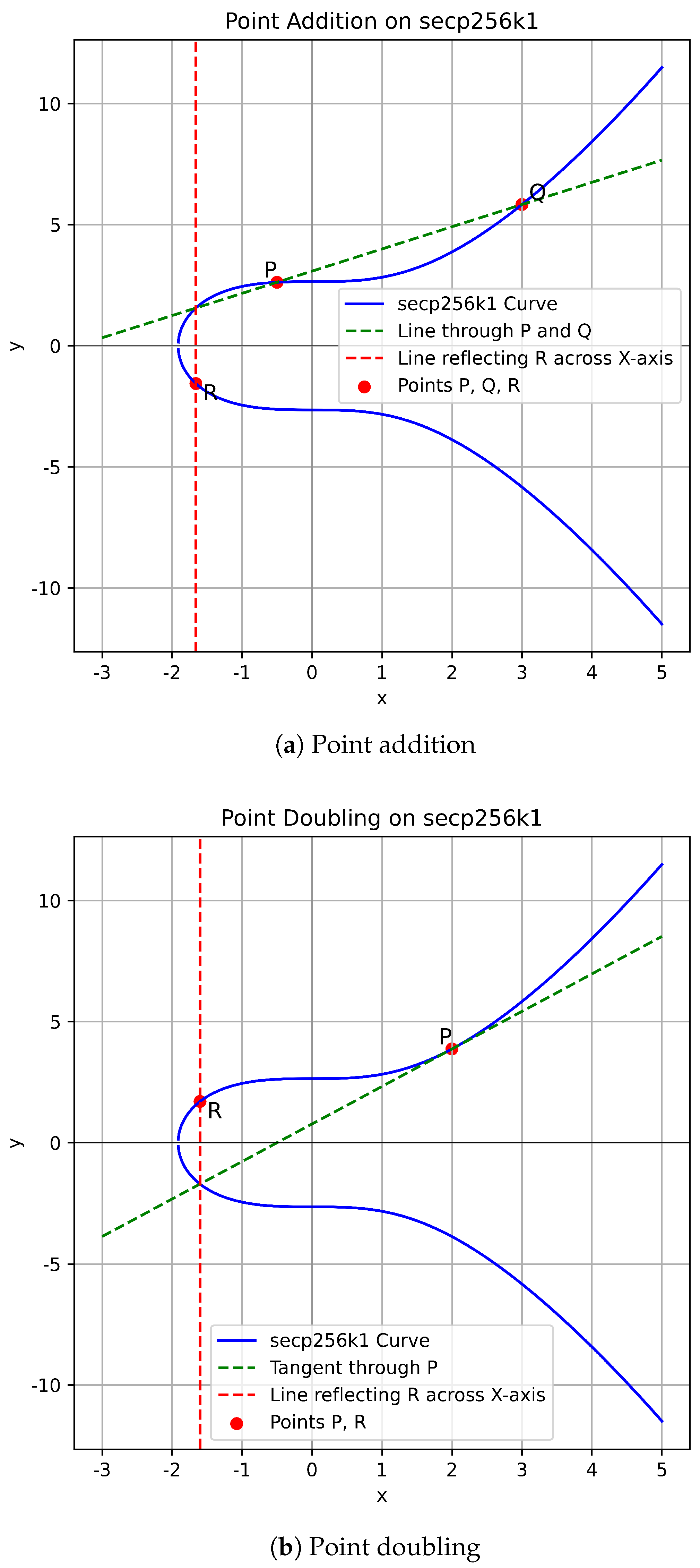
2.1. ECC and Point Operations

Elliptic Curve Cryptography (ECC) is built on elliptic curves over finite fields. It belongs to the public-key cryptography (also known as asymmetric cryptography) domain where a pair of public and private keys is used to encrypt, decrypt, sign, and verify messages. ECC has the advantage of smaller keys for the same security level when compared with other approaches, such as Rivest–Shamir–Adleman (RSA). The intractability of specific mathematical puzzles serves as the foundation for public-key encryption. In ECC, the basic premise is that it is very hard or impossible to find the discrete logarithm of a random elliptic curve point when a base point on an elliptic curve is given. This is known as the “elliptic curve discrete logarithm problem” (ECDLP) [7].
An elliptic curve is represented by a group of points that satisfy a cubic equation over two coordinates x and y, such as
y 2 = x 3 + a x + b
where a and b are two of many more curve parameters on which two parties need to agree before engaging in an ECC scheme. The elliptic curve if defined over F p , a finite field of integers modulo p. This means that a , b , x , y F p and that the field operations available over this field are addition, multiplication, subtraction, and multiplicative inverse (instead of division), all modulo p, where p is a large prime number [8].
For our implementation, we chose the secp256k1 [9] curve defined by the equation y 2 = x 3 + 7 , which is one of the most popular curves, being used by the most dominant blockchain systems in terms of market share: Bitcoin and Ethereum  (https://www.coingecko.com/research/publications/market-share-nft-blockchains accessed on 20 February 2025). As the name suggests, the curve’s key size is 256 bits (for both public and private keys) and is defined over the field F p with p = 2 256 2 32 2 9 2 8 2 7 2 6 2 4 1 .
On top of the four field arithmetic operations mentioned before, the elliptic curve group itself has addition as the characteristic group operation, also referred to as point addition. In elliptic curve arithmetic, the point addition of two points P and Q that are on the curve means finding a point R on the curve such that R = P + Q . Figure 1 shows a visual representation of the point addition (a), and also a special case of addition called point doubling (b), where a point P is added to itself such as R = 2 P .
Point addition can be defined by the following steps:
  • Select two distinct points P and Q on the elliptic curve.
  • Draw a straight line passing through P and Q.
  • Identify the third point of intersection with the elliptic curve, denoted as R.
  • Reflect R across the x-axis to obtain the result P + Q.
Meanwhile, point doubling is defined as follows:
  • Select a point P on the elliptic curve.
  • Draw the tangent line at point P.
  • Identify the second point of intersection with the elliptic curve, denoted as R.
  • Reflect R across the x-axis to obtain the result 2P.
These operations are fundamental to Elliptic Curve Cryptography. They are used in various cryptographic protocols such as digital signatures and key exchange, and most recently in applications involving zero-knowledge proofs (ZKP) [10]. What strengthens the ECDLP problem for these protocols is the order n of the group, another public parameter, which is a large number of size 256 bits in the case of the secp256k1 curve. The final public parameter, a generator point G on the curve, generates all points P that two parties are allowed to use in a protocol for a given elliptic curve such that
P { G ( x , y ) w h e r e x , y F p | G , 2 G , 3 G ( n 1 ) G } n G = G + G + + G
As the elliptic curve group is a finite group but defined over a large-order number (256 bits), the repeated addition that can be seen in Equation (2), also called point multiplication, is the operation that hardens the ECDLP problem, as given a random point P = s G , with G known, it is computationally infeasible for a classic computer to recover s if both s and n are large enough. Furthermore, if we define Multi-scalar multiplication as a function that takes a vector of N scalars (positive integers) and a vector of N elliptic points and performs the vector product of the two, as it can be seen in Equation (3), the resulting point can be any point P defined in Equation (2), thus making it even more difficult for a possible attacker to try and recover any possible value part of the two vectors. The MSM operation is heavily used in ZKP systems, while the special case of N = 2 is used in the Elliptic Curve Digital Signature Algorithm (ECDSA) [11].
M S M ( P , S ) = i = 0 N 1 p o i n t M u l t ( p i , s i )
Function p o i n t M u l t used in Equation (3) is defined in Algorithm 1 and represents the double-and-add algorithm, where both point addition and point doubling are employed in order to compute the point multiplication between a scalar and a point. The for loop iterates m times, where m is the bit size of the scalar s, thus, in our case, iterating for 256 times. Point addition and point doubling on their own are complex operations. In a classical mathematical approach, if we take point addition as an example, computing R = P + Q using their Cartesian coordinates as ( x P , y P ) + ( x Q , y Q ) = ( x R , y R ) is performed through the use of the slope equation that crosses the two points, as depicted in Equation (4).
λ = y Q y P x Q x P x R = λ 2 x P x Q y R = λ ( x P x R ) y P
Algorithm 1 Double-and-add for point multiplication
Input: Point P, scalar s in binary form with m bits
   Let R = O be a point at infinity
   for  i m 1 to 0 do
       R = 2 R ▹ Point doubling
      if  s [ i ] = = 1  then
          R = R + P ▹ Point addition
      end if
   end for
   Return R
Even if the equation seems simple at first sight, the processing unit such as a CPU, or even a GPU, has a difficult time computing a point addition operation, mainly because of the division operation employed by the slope equation. As we operate over a finite field, classic division is not possible, and instead, the multiplicative inverse operation must be used. Even with meaningful research regarding this operation, as well as its optimization for different architectures (CPU/GPU/FPGA), the latency of the current algorithms is high, counting for hundreds of iterations, and increasing with the bit size [12]. As point addition, and similarly point doubling, are repeated multiple times for the computation of a point multiplication, the multiplicative inverse operation becomes a burden for the system, and if we look into a ZKP protocol where a high number of point multiplications are performed (up to 2 20 operations), this results in execution times of seconds and tens of seconds.
One common way to avoid the multiplicative inverse is to switch from Cartesian coordinates (also referred to as affine coordinates) to another system of representation, such as the Jacobian system. This translates our points from a pair of two coordinates to a pair of three, adding more modulo additions, subtractions, and multiplications for computing point addition and point doubling, but without the need to use the multiplicative inverse at each point operation encounter. The multiplicative inverse is used only two times at the end of a point multiplication, or the end of the entire MSM operation, in order to translate the ( x , y ) coordinates from the Jacobian system, back to the affine system [13].
It is possible to also mix the two representation systems, with one point being in the Jacobian system, while the other remaining affine, which gives out better results overall. As we follow Algorithm 1 for our implementation, we implement point doubling using the Jacobian system as the intermediate point R will also be in the same system, while for point addition we use a Jacobian and affine formula, as our intermediate point R will be added with the initial point P, which is given in affine coordinates. The point multiplication unit we implemented for FPGAs does not include a multiplicative inverse module for converting back the coordinates, as we want to offer a flexible design that can be integrated as part of a more complex system, such as a ZKP accelerator for example. Because of that, a system designer can later add such a module to compute back the coordinates either directly in the FPGA or in software on the host application that is part of a hardware–software co-design.

2.2. FPGAs and High-Level Synthesis

FPGAs stand out as revolutionary components in electronics, offering unparalleled flexibility and customization within a single chip, unlike their rigid counterparts, such as CPUs, GPUs, and ASICs. With their configurable logic blocks and programmable network of wires, FPGAs can be tailored to meet the exact requirements of a project. This adaptability enables them to serve a wide range of applications, including real-time signal processing and AI acceleration, positioning them as key players in shaping the future of technology [14]. However, this flexibility comes at a cost. Compared with predefined chips, FPGA design possesses inherent complexity, demanding sophisticated tools and expertise in specific RTL hardware design languages like VHDL or Verilog. The design process within this language is tedious and error-prone, requiring long development and verifying times, which ultimately affects the time to market of the product. Additionally, their power consumption can be higher, requiring careful optimization for energy efficiency.
High-Level Synthesis (HLS) presents a groundbreaking approach to hardware design by bridging the gap between software and hardware [15]. By simplifying the development process and making hardware design more accessible to a broader range of engineers, HLS addresses the challenges of complexity and democratizes hardware design. Despite facing performance and resource utilization challenges, ongoing research in optimization techniques is poised to propel HLS to new heights, unlocking its potential to revolutionize custom hardware design [16]. One popular HLS vendor tool is the Vitis HLS toolchain from AMD-Xilinx, which empowers engineers to exert control over the hardware design using C/C++ pragmas, optimizing parallelism and resource utilization in FPGAs. Because of its free access and open-source libraries that streamline algorithm acceleration and promote efficient hardware design principles, its reach documentation, and the larger community, it makes it the perfect choice for our design tool. In our design approach, we make use of three key paradigms: producer–consumer paradigm, streaming data paradigm, and pipelining paradigm and provide a better view of the task-level parallelism and the hls::task class available in Vitis, which is the main component that we leverage in the design of our RISC point arithmetic units.

3. Related Work

In this section, we discuss FPGA implementations related to the secp256k1 elliptic curve. This includes point arithmetic units and application-specific engines like signature verification engines. Compared with other elliptic curves would not be suitable due to varying latencies and performance arising from different modulo prime number polynomial forms [17]. Much of the available research, to the best of our knowledge, mainly focuses on specific use cases of the ECC arithmetic units, such as signature verification, data encryption, or key generation. In such cases, we attempt to extract, whenever possible, the implementation details of the ECC arithmetic units alone. Otherwise, we present the hardware engine implemented over the secp256k1 curve.
We analyzed articles [6,18,19,20,21,22] that implement ECC arithmetic units or ECC engines using the secp256k1 curve. In [18], the authors propose a high-speed generic ECC point multiplier unit for Weierstrass curves over G ( p ) with modulus size up to 256 bits. The design makes use of a pipelined multiplier, adder, and subtracter that work over the Montgomery domain in order to support multiple curves, and the point multiplication algorithm uses Hamburg’s formula, which avoids the need to schedule both point doubling and point addition (when the current scalar bit is ‘1’) in every iteration. The FPGA-based hardware accelerator [19] implements an ECDSA verification engine for the Hyperledge blockchain. It uses a couple of mathematical tricks, such as the NAF window method and precomputing several values of the point generator G to speed up the point multiplication. Regarding field arithmetic, it uses the Barrett reduction algorithm over general modulo as it is hardware-friendly despite having greater latency. The article in [20] proposes an ECPM core where the sum of residues (SOR) modular reduction and the Residue Number System (RNS) are used for the field arithmetic layer implementation. The authors explore the implementation and scheduling of the modulo operations with one and two multiplication units and also look into different variations in the point multiplication algorithm. In both [21,22], the authors introduce a hybrid approach as an IoT solution. This approach involves a hard processor (ARM) and the programmable logic of an FPGA working together to implement an entire ECDSA core for signing and verifying signatures. The FPGA contains an ECC engine capable of performing point multiplication. Since the application targets the IoT context, the design has a small footprint and implements point addition and point doubling in affine coordinates to keep logic consumption low. However, this results in a more significant latency as the inverse multiplicative must be computed at each iteration in the point multiplication algorithm. The work from [6] describes an ECDSA verification engine within a hybrid database system. The authors initially used the open-source implementation of the ECDSA verification module from the AMD-Xilinx Vitis libraries [23]. Due to the high latency in the original implementation, the authors made modifications. They proposed a new approach by opting for a simple divide-and-conquer method instead of using complex mathematical tricks to speed up point multiplication, which is not usually hardware-friendly. In this approach, the authors split the point multiplication kernel into multiple stages, each processing 256 / n bits from the scalar, where n represents the number of stages. This allowed them to schedule more than one-point multiplication.

4. HLS Abstract Parallel Programming

As mentioned in Section 1, we propose a pipelined processor architecture to process point addition and doubling for point multiplication. Section 5 will detail how this architecture is applied in our case. In this section, we introduce the concepts needed to understand the design choices made. The key aspects we leverage in our design implementation of the point processor architecture are the three paradigms of FPGA high-level programming: producer–consumer, pipelining, and streaming data. One approach to employ all three paradigms is through the use of the HLS dataflow pragma. This pragma instructs the HLS compiler to analyze the loop or function body, extract the graph of potential parallel scheduling, create FIFO/PIPO channels between sequentially called functions, and finally schedule them to run in a pipeline fashion, achieving a pipelined hardware design through task level parallelism.
Figure 2 illustrates the use of pragma HLS dataflow. In this simple example, a top function comprises four tasks. The compiler can schedule these tasks to be processed in parallel based on their input and output dependencies. Scalar arguments can be used as input/output ports, which are automatically converted into channels by the compiler. Functions without dependencies, such as funcB and funcC, are scheduled in parallel to improve performance. On the other hand, funcA and funcD, which act as the initial producer and final consumer and have dependencies, are scheduled in a pipeline fashion to overlap between consecutive streamed inputs, similar to consecutive function calls of the top function in software terms. With an ideal initiation interval (II) of one clock cycle, the top function can process a new element from the vecIn buffer and output a new result to vecOut every clock cycle. Even if functions have latencies greater than one cycle, as long as the load–compute–store model is respected and each function still has an II of one, the entire design can process and output an element every clock cycle. The latency of the functions affects the depth of the main pipeline, thereby impacting the timing of the first output result.
In Figure 3, we see an overview of a classic RISC processor pipeline. Ideally, With the HLS pipeline pragma used to implement a processor pipeline, each stage implemented as a task should be written with an initiation interval (II) of one to start a new instruction each clock cycle. However, real-case scenarios involve data dependencies and data access delays, leading to data hazards. Stalling and bypassing are commonly used to address these issues. Data dependencies would be automatically detected by the Vitis HLS compiler, which can add permanent stalling logic to resolve the hazards (the design would stall regardless of an actual hazard encounter, as this would ensure no possible deadlock). Bypassing can be incorporated using dependency pragmas to indicate the absence of actual dependencies within a loop or between consecutive loop iterations and through if-else constructions and global static variables so that stages can access commonly needed data when available. However, one drawback is the high combinational latency required to verify potential hazards and forward available data within one cycle, resulting in long clock periods (over 10 ns from our experiments).
The HLS dataflow paradigm allows for feedback channels between producer and consumer tasks, ensuring bypassing. However, the compiler assumes that each function is entirely independent, leaving the designer responsible for handling dependencies. Implementing logic for data hazard detection and forwarding inside a function can guarantee a good initiation interval (II) and higher frequencies. Specific guidelines must be followed when using the dataflow model in Vitis HLS to avoid unpredictable compiler behavior and worse performance. For instance, while this is allowed in version 2023.2 of the tool, in older versions, task feedback through bypassing is not allowed. To get by this limitation, we suggest using the hls::task library for both point adder/doubler units and the point multiplication scheduler. This library allows for a clearer description of task-level parallelism, similar to classic RTL approaches. Listing 1 illustrates the usage of the hls::task library to describe a diamond-shaped task structure, as shown in Figure 2, where each function performs different operations on the inputs and outputs them to the next task.
Listing 1. Code example of using the hls::task library with Vitis HLS.
void funcA(hls::stream<int>&in, hls::stream<int> &out1, hls::stream<int> &out2) {
  int data = in.read();
  if(data%2){
    out1.write(data+1);
    out2.write(data+2);
  }else{
    out1.write(data+2);
    out2.write(data+1);
  }
}
void funcB(hls::stream<int> &in, hls::stream<int> &out) {
  out.write(in.read() >> 1);
}
void funcC(hls::stream<int> &in, hls::stream<int> &out) {
  out.write(in.read() << 1);
}
void funcD(hls::stream<int> &in1, hls::stream<int> &in2, hls::stream<int> &out) {
  out.write(in1.read() + in2.read());
}
void top(hls::stream<int> &in, hls::stream<int> &out) {
  hls_thread_local hls::stream<int> s1;
  hls_thread_local hls::stream<int> s2;
  hls_thread_local hls::stream<int> s3;
  hls_thread_local hls::stream<int> s4;
  hls_thread_local hls::task t1(funcA,in,s1,s2);
  hls_thread_local hls::task t2(funcB,s1,s3);
  hls_thread_local hls::task t3(funcC,s2,s4);
  hls_thread_local hls::task t4(funcD,s3,s4,out);
}
The tasks can be categorized into control-driven tasks (funcA) or data-driven tasks (funcB/C/D). Data-driven tasks are executed every time data is available on the input ports. This type of task is used in our execution unit, processing new data each clock cycle as long as data is available. Control-driven tasks can start execution based on defined conditions or can follow different execution paths based on different conditions between consecutive runs. They can be coupled with non-blocking reads of input ports or static variables to react differently between consecutive executions, even without data on the input ports. After a task finishes execution, it restarts immediately from the beginning. However, there is a limitation with the hls::task library as tasks cannot access global variables. We use a workaround to handle shared memory between pipeline stages by declaring the memory and defining control logic for it inside one task, and using streaming channels for communication between tasks that need to read or update the memory.
The hls::stream_of_blocks library is a key component in our design, allowing the streaming of data arrays with explicit control and flexibility. It provides higher performance and a smaller storage size compared with PIPO streams. This library facilitates synchronization between producer and consumer, increasing throughput. In our case, it acts as a small cache memory between task processes, optimizing data processing. Listing 2 shows a high-level usage of the library where a producer streams an entire block of N integers at each iteration. As at the end of every iteration the producer releases the lock, the consumer can immediately acquire a read lock in order to process locally the available data in its current iteration, after which it also releases the lock that can now be acquired again by the producer to stream new data. Thus, the execution of the two processes is overlapped while both processes can produce and consume larger amounts of data at each iteration. For our case, we work with 256-bit values instead of integers; N is three, the number of coordinates that a Jacobian point has, and M is equal to the defined size of the batch of points that we can process. We evaluate multiple batch sizes of 8/16/32/64 points that a point adder processor can process in pipeline.
Listing 2. Code example of using the hls::stream_of_blocks library with Vitis HLS.
typedef int buf[N];
void producer (hls::stream_of_blocks<buf> &s) {
  for (int i = 0; i < M; i++) {
    // Allocation of hls::write\_lock acquires the block for the producer
    hls::write_lock<buf> b(s);
    for (int j = 0; j < N; j++)
      s[j] = ...;
    // Deallocation of hls::write\_lock releases the block for the consumer
  }
}
void consumer(hls::stream_of_blocks<buf> &s) {
  for (int i = 0; i < M; i++) {
    // Allocation of hls::read\_lock acquires the block for the consumer
    hls::read_lock<buf> b(s);
    for (int j = 0; j < N; j++)
       int t = s[j];
    // Deallocation of hls::read\_lock releases the block for the producer
  }
}
void top(...) {
  hls::stream_of_blocks<buf> s;
  producer(s);
  consumer(s);
}

5. Design of Point Processing Units

In this section, we cover the architecture for the point adder processor and the point multiplication scheduler, detailing the use of HLS libraries for implementation. Both units have defined batch sizes, with evaluations for batch sizes of 8, 16, 32, and 64 points per batch. Our hardware kernel doesn’t currently include a conversion unit for bringing points back to affine coordinates, as this is planned for future use as part of a larger system. This approach allows for flexibility in handling conversions through the host application as part of a comprehensive, heterogeneous solution.

5.1. Point Multiplication Scheduler
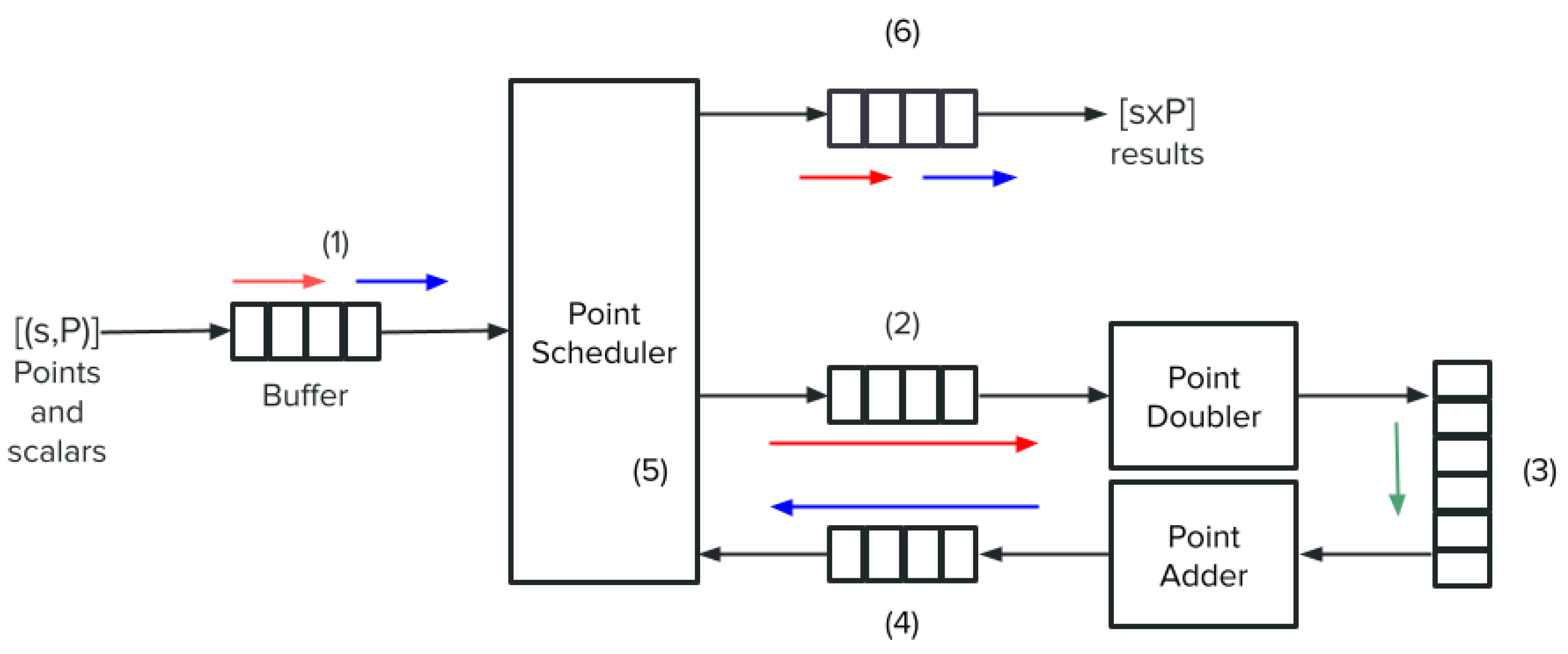
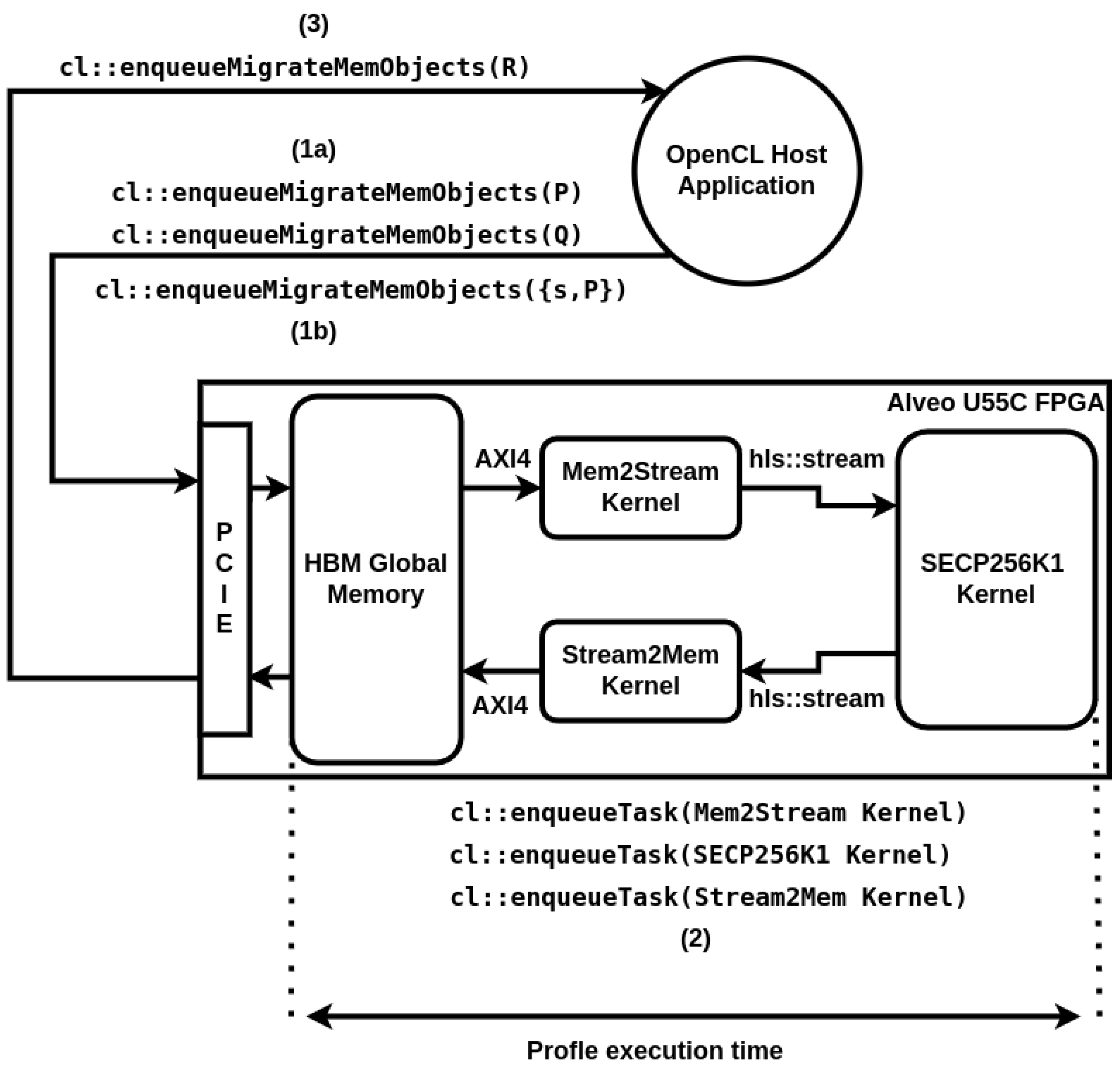
Figure 4 shows the top hardware kernel architecture, with the three major components: the point multiplication scheduler, the point adder, and the point doubler, and the corresponding connections and buffers between them. The flow of the hardware kernel in computing the s × P point multiplication of multiple points, using Algorithm 1, where s represents a scalar, and P represents an affine point, is the following:
(1)
When ready, the point scheduler will read two batches of N pairs of points and scalars, where N can be 8/16/32/64. The points are read in their affine form, so one pair will have a total of 768 bits: two 256-bit coordinates and one 256-bit scalar. As we want to conserve resources, we use a single 256-bit hls::stream interface for streaming each pair.
(2)
When the point double unit is ready, the point scheduler sends the first batch to it through two 256-bit hls::stream interfaces. One interface is used to stream the original pairs inside the batch, as we need the unmodified points P for the point addition operation, and we also need the current value of the scalar s. The second interface streams the intermediate point R, which will become our result. This point is also streamed as a pair of three 256-bit values, which represent the three coordinates in the Jacobian system. In the first iteration of the double-and-add algorithm, R is streamed with initial values ( 1 , 1 , 0 ) for all points in a batch. The unit doubles R at each encounter.
(3)
When the point doubler finishes the first batch of points, and the point adder unit is/becomes free, it streams through two 256-bit hls::stream interfaces as well the ( s , P ) and R pairs of 256-bit values. The point adder will use both R and P values to update R, but only based on the most significant bit of the scalar s, in which case it should be ‘1’. Otherwise, for an MSB of ‘0’, R is not modified. In the meantime, when the point doubler finishes sending the first batch of points to the point adder, it can start reading and processing the second batch from the point scheduler.
(4)
Once the point adder finishes the first batch, it forwards it back to the point scheduler unit, similar to the point doubler, using two hls::stream interfaces: one for the ( s , P ) pair and one for point R. As mentioned before, point R is updated only if MSB of s is ‘1’; otherwise, R is streamed with the same values it comes with. For the ( s , P ) pair, point P is not modified, but scalar s is shifted to the left by one bit so that at the next encounter, the point adder can check the next MSB. This is applied to all scalars in a batch. Similarly to point doubler, once the first batch si dispatched, the point adder is ready to receive the second batch from point doubler immediately.
(5)
The point scheduler waits for the first batch to come back, and as soon as data are available on the hls::stream interfaces connected to point adder, it forwards the batch of pairs immediately to the interfaces connected to point doubler, which in turn can start reading them when it becomes free. Once the first batch is dispatched, it proceeds similarly with the second batch and keeps it until point doubler can take it. The point scheduler has an internal counter, which is incremented after both batches are dispatched to the point doubler. This process of cycling the two batches through the two point arithmetic units is repeated 255 times, as described in Algorithm 1 (excluding the initial cycle in which R starts with initial values).
(6)
After the internal counter of the point scheduler reaches the 256 iterations, the point scheduler will forward the two batches, one by one, through the output interface, which is a single 256-bit hls::stream interface that will stream the result point R with its three 256-bit coordinates in the Jacobian system. The point scheduler dispatches the first batch as soon as it is available on the interface connected to the point adder, and afterward, it proceeds similarly once the second batch is also available. After dispatching the last batch, it immediately forwards a new pair of batches, if available, repeating the entire flow starting from point (1).
The point scheduler relies on the hls::task and hls::stream_of_blocks libraries for seamless data transactions between the point arithmetic units. Figure 5 provides an overview of the scheduler. It utilizes 256-bit hls::stream interfaces for input and output ports. The upstream buffer holds new batches of points and scalars, while the downstream buffer receives the results of the multiplications. Buffers are placed between the scheduler and the point arithmetic units to prevent deadlocks or bottlenecks. Internally, multiple producer and consumer tasks use the stream of blocks model to read or write N blocks effortlessly. Overlapping executions between producer and consumer tasks is achieved through the hls::stream_of_blocks library.
When the point scheduler unit is idle, the Load Task reads batches of N point and scalar pairs through an hls::stream interface, converting them into hls::stream_of_blocks. These act as small dual-port memories, allowing the Schedule Task to access the previous block as soon as it’s written, facilitating continuous operation without waiting for an entire batch. Tests on memory depth, ranging from two to N blocks, showed identical maximum throughput, indicating no performance gain from larger memory depths. Thus, to optimize resource use, all hls::stream_of_blocks channels are set to the minimum required depth. The Schedule Task connects the Load Task and Write Task through channels, serving both as a consumer and producer. It cannot read data from its channel while the Load Task has a lock but can write to the Write Task’s channel. Once the Load Task unlocks, the Schedule Task and Write Task can read available data. This setup maintains a steady flow of data blocks from the upstream module to the point doubler.
After sending two batches of data, the Scheduled Task’s internal counter increases, and the Schedule moves to the next state. Here, it acquires a read lock on the Read Task’s channel and a write lock on the Write Task’s channel. The Read Task retrieves available data from point adder buffers and transfers them to the Scheduled Task. The unique locking mechanisms of the tasks eliminate the possibility of a deadlock as long as the Read–Schedule–Write order is maintained after dispatching new data batches:
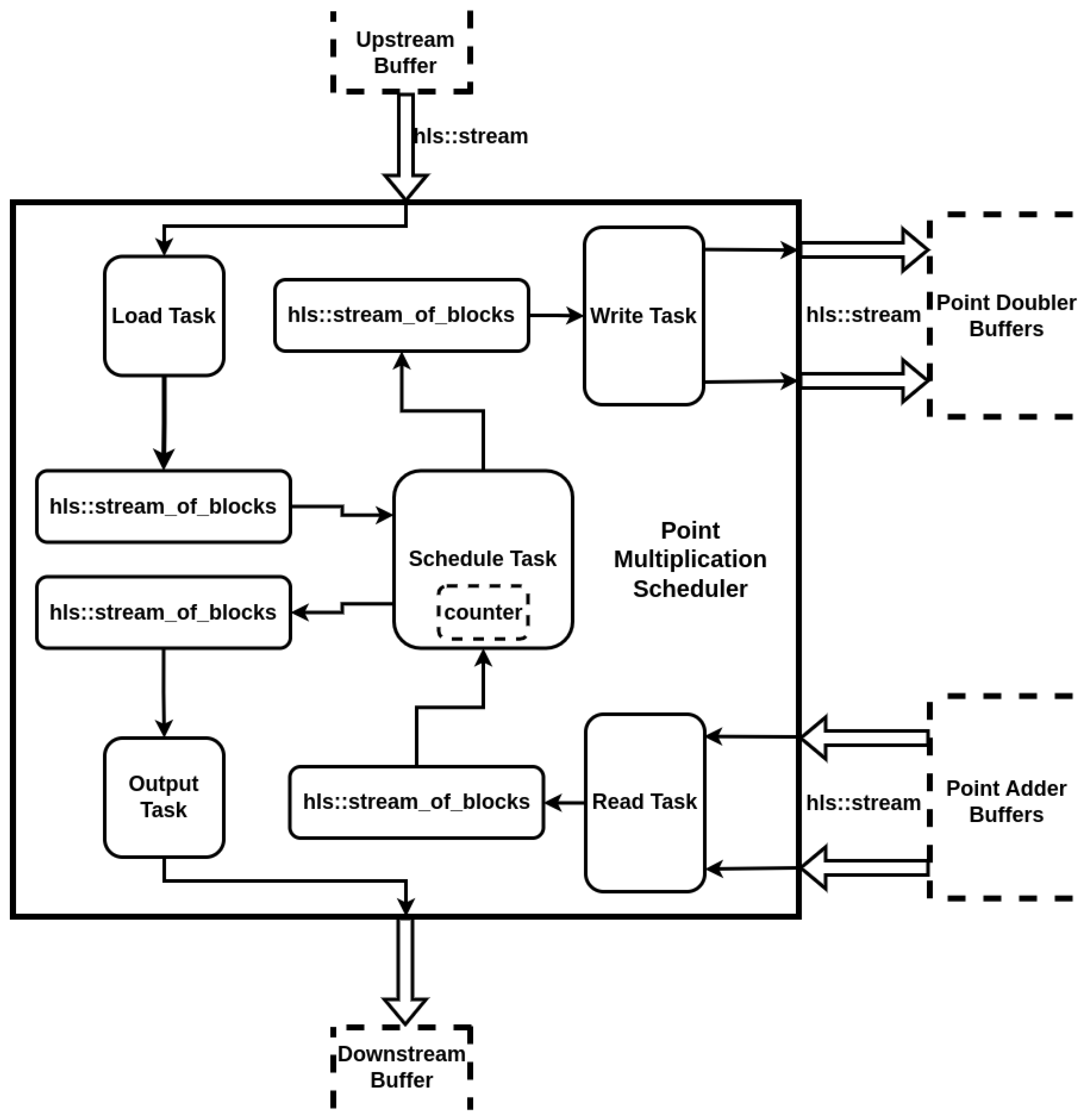
  • With the Schedule and Write Task either free or occupied dispatching blocks of data, the Read Task will see data available on its interface from the point adder, so it can acquire a lock first on its channel with the Schedule Task as the Schedule Task is either free or busy sending blocks of data on its other channel connected to the Write Task
  • When the Schedule Task is free, it will be able to acquire a read lock on the channel connected to the Read Task only when the Read Task finishes an iteration out of 2 N (we have two batches that need to be read) of writing. While the Read Task reads the next block of data, it has to release the write lock of the channel, meaning that the Schedule Task can now acquire it and read the block of data.
  • As the Schedule Task finishes reading a block of data, it will release the channel connected to the Read Task and acquire the channel connected to the Write task to dispatch the fresh block of data. This allows now the Read Task to write lock the channel again to push the next block of data.
  • After the Schedule Task finishes pushing its current block of data to the channel connected to the Write Task, it has to release it in order to return to the channel connected to the Read Task to get a new block of data. This means that the Write Task can now read lock the channel and read the block of data in order to push it to its stream interface connected to the point double buffers.
  • As the Write Task finishes reading a block of data, it has to release it as well in a move to push it to the stream interface, meaning that the Schedule Task can write lock it again in order to push a new block of data.
The Read–Schedule–Write process is repeated until the counter reaches 256 iterations. At this point, the Schedule Task forwards the final results to the Output task instead of the Write Task, changing the flow to Read-Schedule-Output. Once the 2 N blocks of data are sent, the Schedule Task can immediately start reading new batches of points and scalars. The Load Task, running concurrently with all the other tasks, may have already pushed new data into its channel for the Schedule Task to access. The read-and-write lock mechanisms ensure that a lock is not maintained if the channels are empty or full. This behavior is modeled for any two producer–consumer pairs of concurrently running tasks connected through a hls::stream_of_blocks channel, ensuring that a slower or faster consumer/producer will not block the channel indefinitely.

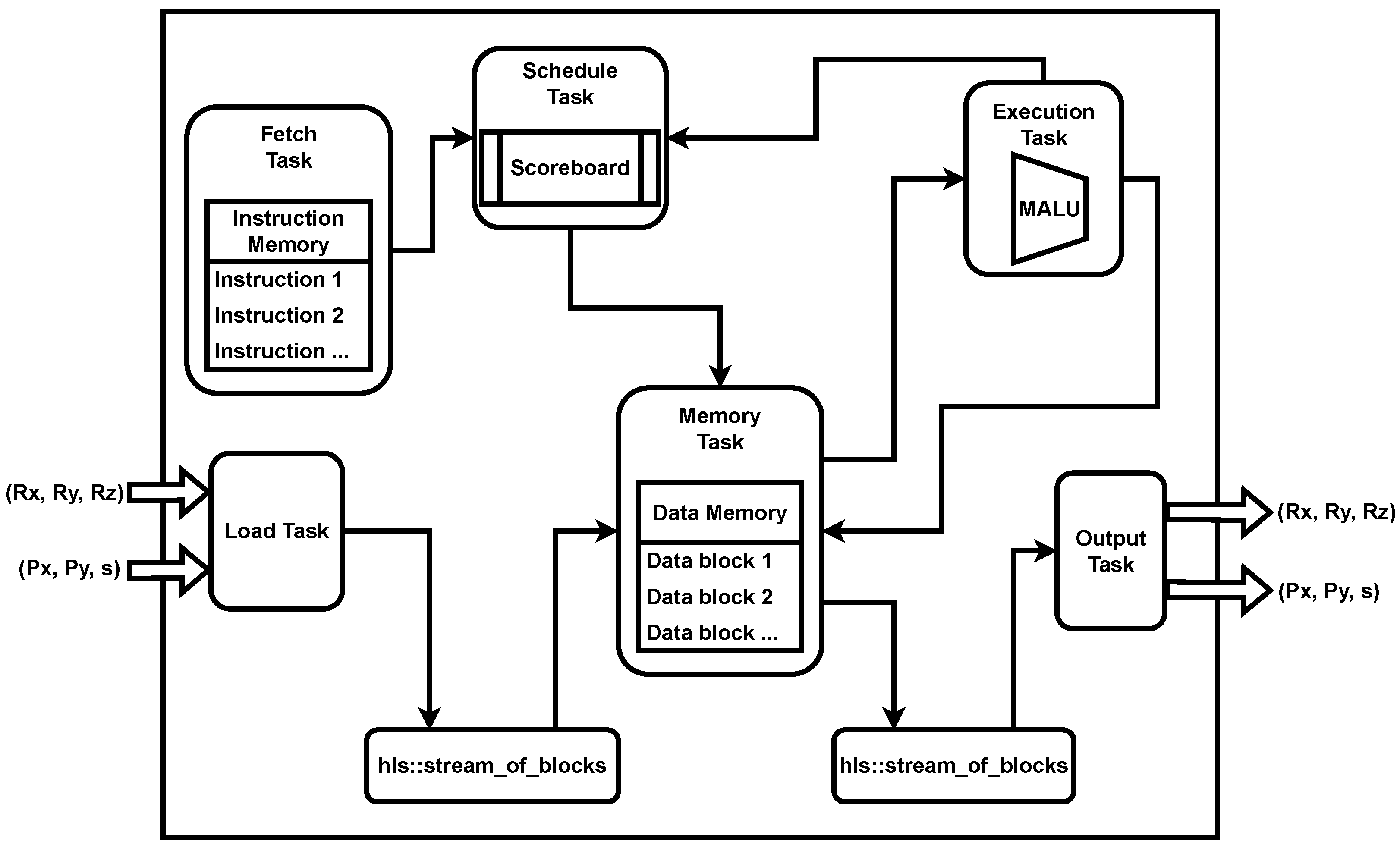
5.2. Point Arithmetic Processor

We use a Batched Point Arithmetic Processor (BPAP) for efficient point addition and doubling operations. This processor handles field arithmetic operations for an entire batch of N points, optimizing execution unit utilization. The BPAP architecture follows a Reduced Instruction Set Computer (RISC) design, similar to that of RISC-V [24]. Our architecture, depicted in Figure 6, is based on the three HLS libraries used to design the point multiplication scheduler. Similar to RISC-V, we have a Fetch Task that retrieves a new instruction from the instruction memory each cycle and sends it to the Schedule Task. Our MALU (Modulo Arithmetico-Logical Unit) performs field arithmetic modulo operations over 256-bit numbers, resulting in a delay before a result is available to be read. In this case, we must stall the execution of any new instruction if a data hazard occurs. The Schedule Task detects data dependencies by maintaining a scoreboard with all result addresses awaiting output from the Execution Task unit. If the addresses of a current instruction’s source operands are not in the scoreboard, it indicates no data dependency, and the instruction can be forwarded from the Schedule Task to the Memory Task. If one or both operands’ addresses are found in the scoreboard, the pipeline execution is stalled until the Execution Task signals that the blocked operands can now be read and the pipeline execution can resume.
When an instruction can be executed, the Schedule Task sends it to the Memory Task. In the Memory Task, we store all intermediate values through a data memory, which functions as a Register Read stage. Unlike a classic processor, we use only data memory and define our instruction set to work directly with memory locations. After reading the source operands’ values from the data memory, the values, along with the result address and the operation type (addition, subtraction, or multiplication), are sent to the Execution Task. The MALU in the Execution Task is pipelined with a one-clock cycle interval, allowing it to process a new pair of inputs every clock cycle. After the MALU unit outputs a result, the value and the result address are sent back to the Memory Task to be stored. Simultaneously, the result address is also sent back to the Schedule Task to update the scoreboard table and eliminate any potential stall caused by a data hazard. The Load Task and Output Task use the memories created by the hls::stream_of_blocks library as small cache memories. They cache the next batches of points so that the BPAP unit can start processing them immediately when it finishes the current batch. BPAP has two pairs of 256-bit hls::stream interfaces. On the input side, one interface loads the current value of the temporary R point, while the second interface loads the ( s , P ) pair. On the output side, one interface outputs the updated value of the R point, while the other interface outputs the ( s , P ) pair. All four interfaces stream blocks of data of 768 bits. For point addition, s is shifted to the left by one bit, while no modification is performed for point doubling. Also, for point addition, based on the most significant bit (MSB) of s, the R point is updated or kept as it was received. The received values of s, P, and R are stored in reserved locations of the data memory to retain the original values. The differences between a BPAP instantiated as a point adder and a BPAP instantiated as a point doubler lie in the instruction memory containing the field arithmetic operations that implement the specific point operation. Figure 7 shows the translation between the point doubling formula for a short Weierstrass curve using the Jacobian system representation. Similarly, the same procedure is applied for point addition using the formula of adding two points, where the Z coordinate of one point is always 1. We use the madd-2007-bl and dbl-2009-l formula (https://www.hyperelliptic.org/EFD/g1p/auto-shortw-jacobian-0.html 20 February 2025).
Instructions are 16-bit-long and contain the addresses of the two source operands, the result address, and the operation type, each codified on 4 bits. The instruction memory is bound to a ROM memory with one port. In order to better utilize the data memory space, we rearranged and modified the intermediate operands in the formulas to utilize as little memory as possible. As shown in Figure 7, addresses $ 0 , $ 1 , $ 2 store the point that needs to be doubled and will also store the result. Besides that, we only use addresses $ 3 , $ 4 , , $ 9 for the intermediate calculations. Other than this, we use three more address locations to store the values of the ( s , P ) pair, and we also provide three extra addresses for future use and better partition our data memory into blocks of 16 addressable locations. We also define store and load instructions, which flag the beginning of a new batch and the end of the current batch. Here, we define s t o r e ( P , Q ) , where P is the 768-bit data block containing ( P x , P y , s ) and Q is the 768-bit data block containing ( R x , R y , R z ) . We parallel stream both blocks in the hls::stream_of_blocks channels through the Load Task into our data memory. Similarly, l o a d ( P , Q ) , P , Q will parallel stream the updated values of the two blocks of data through hls::stream_of_blocks connected to the Output Task and further to the downstream module.
The Fetch Task runs continuously and loops through the defined micro-code indefinitely. It sends the sequence of instructions to the Schedule Task and then to the Memory Task. When the pipeline encounters the first set of points after a global reset or hardware kernel start-up, it will stop until the Memory Task receives data from the Load Task through the block channel. This is because the store instruction puts the Memory Task in a state where it reads the channel using a blocking read method, ensuring that no execution starts until a set of points is loaded into the main memory. When loading the set of points, the main difference between a point adder instantiation of BPAP and a point doubler instantiation is that for point addition, we need to store the Q block of data (containing ( R x , R y , R z ) ) twice at different locations, essentially creating a copy of it. One copy will be updated with the results of the point addition, while the other will remain unchanged. Depending on the most significant bit (MSB) of the scalar s during the load instruction, we choose either the updated copy or the original copy to adhere to the double-and-add algorithm. Another difference during the load instruction for the point adder instantiation is that we also have to handle the case of addition with the origin point (essentially an addition with 0). In this case, we must send the coordinates of P through the interface of point R (assuming that point P, being a public key, will also be different from the origin point). The current implementation of BPAP performs the complete addition regardless of the value of the MSB of s or whether the R point might be the origin point, because we process an entire set of points for which we cannot know these values in advance. To ensure a smooth flow in the pipeline, we prefer to schedule all points as soon as possible and address these aspects in the load phase at the end of the instruction micro-code. This approach is also more cost-effective in terms of resource consumption for implementing verification logic.
For the batch aspect of BPAP, we defined point batching as executing the current instruction N times, where N is the number of points in a batch. This allows us to share the MALU unit in the Execution Task, as the same operation will be scheduled N times, for every point. Another advantage is that once data dependency is resolved, it will be resolved for an entire set of N intermediate values, meaning we can stream N operations in pipeline through MALU. In order to allow for this kind of batch execution, we also had to provide a data memory large enough to accommodate N points in a batch. This means that 16 addresses are defined for storing initial, intermediate, and final values for a single point. Depending on the value of N (8/16/32/64), our data memory will have 16 × N locations.
AMD FPGA BRAM memory blocks can be configured to use different data widths but are bounded by a data width maximum of 72 bits. As our values are 256 bits in size, for efficient usage, we split each 256-bit word over 64-bit chunks and store each chunk of a value at the same address of 4 individual BRAM memory blocks for fast parallel access when we need to read or write an entire 256-bit value. As we define that each point in a batch of N points will have its own data memory region and that for each individual point, our processor needs 16 addresses to compute the intermediate and final values, the total amount of memory utilized is computed as ( 16 a d d r e s s e s × 4 c h u n k s × N p o i n t s × 64 b i t s ) . For example, for the upper case of 64 points per batch, we utilize 32KB for the data memory. We also configured the BRAM memory blocks as true dual-port memories in order to perform parallel read and write requests.
In Figure 8a, the abstract pseudo-code for implementing the BPAP unit is shown. The Fetch Task handles fetching, decoding, and encoding an instruction with translated addresses before sending it to the Schedule Task. The Fetch Task is pipelined with an II of one clock cycle. It streams the same instruction N times with correctly translated addresses for each of the N points. Once the current instruction has been streamed N times, the Fetch Task proceeds to the next instruction in memory. This process is repeated for all instructions in memory. After completing a round of instructions, the program counter is reset to zero, and the entire operation starts again for a new batch. The procedure allows us to use a small memory for storing instructions, but it requires logic to translate virtual addresses into real physical addresses. The Schedule Task keeps track of data hazards in the scoreboard table based on these real addresses. In the pipeline, tasks run concurrently, handling different instructions at a given moment. For example, the Memory Task can read N pairs of values, while the Execution Task simultaneously executes N operations in a pipeline fashion. Figure 8b shows a visual representation of how, at each current instruction, which is repeated N times, we read the values of the source operands and afterward write the returned result N times for every point. The Schedule Task is also pipelined with an II of one cycle and a depth of three stages, which are the following:
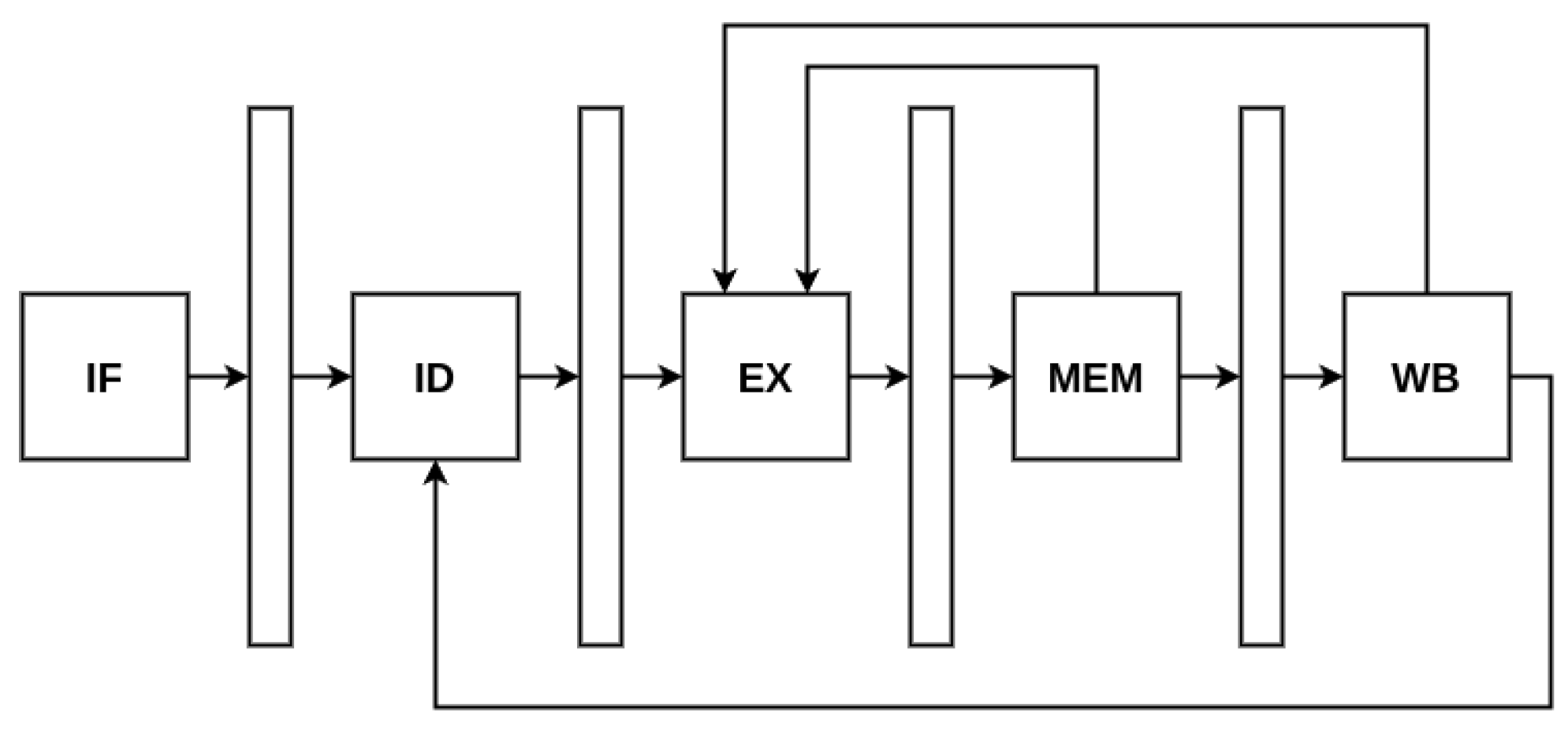
  • Read any new results being completed from the Execution Task and update the scoreboard accordingly (mark the result address as being free)
  • If there is an instruction being stalled, verify the updated scoreboard and see if it can be released (in which case we mark the result address as being busy until we obtain its result), otherwise return and wait for the Execution Task
  • If no instruction has been blocked, then read the new instruction coming from the Fetch Task and verify if it can be released immediately based on the scoreboard or needs to be stalled. If it can be released, then we will mark its result address as busy.
The scoreboard tracks memory location availability in a register, sized by multiplying the number of intermediate ECC point addresses by the batch size (in this case, N × 16 ). It uses ‘1’ and ‘0’ to indicate busy or free locations, respectively. “Busy” indicates a location is being updated by the MALU unit during an Execution Task, while “free” means the location is unused or has been updated. The system operates on an in-order architecture with just one MALU unit, allowing the scheduling of only one operation per clock cycle. The MALU unit, optimized for operations like addition, subtraction, and multiplication, employs a 45-stage pipeline with an initiation interval of one clock cycle. It features a consistent depth across different operations. Specifically, for 256-bit multiplication, it uses a Karatsuba algorithm [25], along with a modulo reduction for the secp256k1 curve, while addition and subtraction leverage standard C++ operations, with optional modulo correction. The implementation strategy for adders and subtractors is determined by the HLS compiler based on set performance objectives, avoiding specific optimizations. All operations are tied to DSPs for enhanced frequency and to conserve FPGA resources.
In final remarks on the point arithmetic processor, it is noted that the Memory Task is not pipelined and has a three-clock-cycle initiation interval for the modulo arithmetic instructions. The data memory utilizes a true dual-port BRAM, preventing concurrent reads and writes. Prioritization is given to writes in this control-driven task. During task execution, a check is made for results from the Execution Task to update memory first, followed by checking for incoming instructions from the Schedule Task to read and forward their values to the Execution Task. The initiation interval increases for load and store instructions due to the additional delays incurred from data memory and hls::stream_of_blocks channel access, specifically 6 clock cycles for load and 9 for store instructions. While the rise in II is notable, these instructions only constitute 10% of the entire micro-code and occur at the beginning and end of processing a batch of N points. Currently, the Memory Task is the primary bottleneck in the BPAP unit, as it prevents achieving an optimal II of one clock cycle, unlike other tasks.

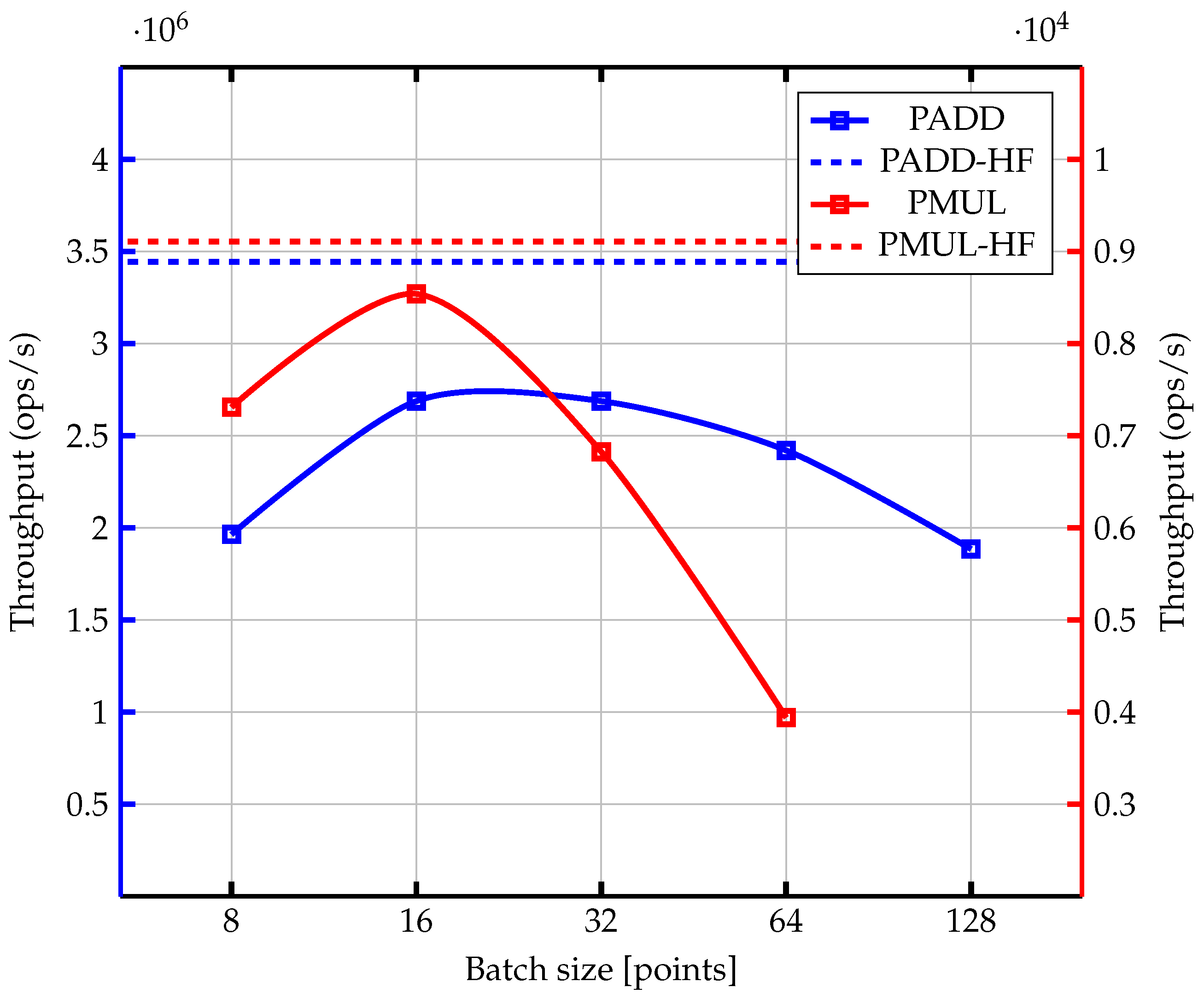
6. Results and Discussion

The evaluation of both the BPAP unit and the complete point multiplication architecture was conducted on an Alveo U55C FPGA board, leveraging the UltrascalePlus architecture from AMD-Xilinx. This board interacts with a Linux Server through PCIe, facilitated by an OpenCL host application. The server utilizes an Intel Xeon CPU E5-2630 v4 at 2.20GHz with 64 GBs of RAM. We used the Vitis 2023.2 ecosystem for the development of the hardware kernels and host application. A static shell recommended by AMD-Xilinx for this model was configured on the FPGA for deploying and interacting with hardware kernels. Additionally, the Xilinx Runtime library (XRT) (https://xilinx.github.io/XRT/master/html/platforms.html accessed on 20 February 2025) software stack was installed for FPGA management and usage. The OpenCL host application is responsible for handling data migration to the FPGA’s global memory, enqueuing hardware kernel execution, and reading back results. We created two additional hardware kernels, Mem2Stream and Stream2Mem so that our BPAP unit and Point Multiplier can access the FPGA’s global High Bandwidth Memory (HBM). These kernels bridge the AXI4 protocol (the only way to access the HBM global memory) and the hls::stream protocol for data streaming between our kernels and the global memory. Figure 9 shows the main flow of our benchmarking setup. The SECP256K1 blackbox represents either a BPAP kernel configured to execute the point addition formula or the full point multiplication kernel.
We profile the execution time of the BPAP and the point multiplication during the enqueueTask phase (2). This setup will allow us to see the raw throughput inside the FPGA logic with a small overhead. We provide separate time recordings for reference for the host to FPGA (1a/1b) and FPGA to host (3) migration time. We profile multiple batch configurations for BPAP and the point multiplication kernels: 8/16/32/64/128 points per batch for BPAP and 8/16/32/64 points per batch for the point multiplication architecture. We run ten consecutive tests for each batch size and provide the mean average execution time recorded.
Table 2 shows the total consumption of the two main kernel designs described in this article for different batch sizes: PADD-BX (BPAP unit configured as Point ADDer for X points per batch) and PMUL-BX (point multiplication kernel configured to process X points per batch). For all kernels, we configured the HLS compiler to use the Congestion_SSI_spreadLogic_high implementation strategy and the Flow_PerfOptimized_high synthesis strategy. As the batch size increased, the toolchain could not reach the desired frequency, as we can see for BPAP with a batch size of 64 points and greater, and for the Point Multiplier, with a batch size of 32 and greater. Based on the throughput obtained from each kernel, we selected the highest performer and re-run the implementation phase with an increased frequency until we hit the maximum possible value. For designs PADD-HFB16 (HF-high frequency) and PMUL-HFB16, we obtained 385 MHz and 320 MHz, respectively. For both kernels, the resource consumption represents the values of the stand-alone kernel as depicted by SECP256K1 from Figure 9. The two additional kernels, Mem2Stream and Stream2Mem used as bridges for access to the global memory have an additional overhead and use a combined total of 6062 LUTs, 9594 FFs, and 16 BRAMs, running at the same frequency as the BPAP or point multiplication kernels. For the point multiplication kernel, the resource consumption represents the total combined resource consumption of the point scheduler and the two BPAP units configured as Point Doubler and Point Adder, as shown in Figure 4.
In Figure 10, the throughput of each PADD (in blue) and PMUL (in red) design of Table 2 is shown, plotted as a continuous line connecting all configurations presented in the mentioned table (8/16/32/64/128 points per batch). The high-frequency (HF) variants are the 16 points per-batch configurations implemented at the highest possible frequency we could obtain during implementation and are shown as horizontal dashed lines. For the HF variant, we chose the 16 points per batch configurations as these obtained the best throughput given the same implementation frequency, so intuitively, it made sense to push for the maximum possible frequency for these designs to see the best possible throughput we could achieve. The PMUL-HFB16 variant (clocked at 320 MHz) achieved a maximum throughput of 9108.29 point multiplications per second, equivalent to 853.90 KBs/s in data throughput. The PADD-HFB16 variant (clocked at 385 MHz) reached a throughput of 3,444,480.54 point additions per second, equivalent to 315.35 MBs/s in data throughput. Increasing the batch size for the PMUL designs does not result in an anticipated increase in throughput due to the total delay encountered for processing a single iteration of the double-and-add algorithm being equal to the total combined delay of the point adder and point doubler units, even if there are two batches processed independently on each unit. The point scheduler still has to wait for both batches to pass through both point arithmetic units. With the increase in the batch size, the delay per unit also increases.
In Table 3, we compare our high-frequency designs with those of related works in Section 3 for ECC point multiplication and addition. Figure 11 shows the visual comparison of TPS between all designs for both point multiplication and point addition modules. Figure 12 shows the area comparison with respect to FFs, LUTs, and DSPs for the ECC point multiplication designs where data were provided as such. In the case of [21], the area was provided as the Intel-specific ALM structure, which offers a different granular level compared with the AMD FPGA, and without having the design, it is hard to estimate exactly how many LUTs and FFs were used as ALMs can be configured to be used as either one 6-input LUT or two 5-input LUTs [26]. Our designs consume more logic resources but achieve higher frequencies using the HLS parallel task abstraction programming method. We achieve a speed-up of more than 4.5× for point addition and a speed-up of at least 1.4× for point multiplication compared with other works. However, our point multiplication kernel is less efficient in terms of area usage.
As our point arithmetic processor is completely implemented in HLS C++ and its design is modular, it can be easily customized to support different elliptic curves, field sizes, and point operations formulas through C++ techniques such as templates or object-oriented programming polymorphism. Of course, this flexibility can be applied within the static implementation (compilation time) of the design into the FPGA, where for each field size, elliptic curve, or operation formula modification, even through templates or class polymorphism, the design implementation must be run again. For a flexible, dynamic runtime approach, the design extension imposes a challenge, as all the internal units of BPAP work per a defined datapath size. Supporting multiple field sizes at runtime becomes problematic from this point of view. One solution would be to support a single large datapath size (such as 1024 bits) so that any field size can be supported through this large datapath size, even if, for the case of secp256k1, only 256 bits would be used. Increasing the datapath size would also increase the routing congestion and critical path delay, affecting the frequency achieved. Another challenge would be supporting different elliptic curves where different optimized modular reductions must be employed. Thus, one must use MALU units supporting each optimized modular reduction function, and this will increase area usage and lower the overall frequency of the design, thus affecting the throughput. The point addition and point doubling formulas for different elliptic curve forms (Weierstrass, Montgomery, Koblitz, etc.) or different coordinate representation systems (affine, Jacobian, etc.) can be easily changed at either compilation or runtime as the formulas are implemented as instructions in memory, which can be easily overwritten when needed.
For future directions of improvement of BPAP, a multi-core design can approached, as for the AMD U55C FPGA that was used during our tests, we estimate that up to 8 such kernels can be instantiated to run in parallel. Further improvement could come from also applying modern CPU techniques such as out-of-order execution where one could compute the intermediate values of the point addition formula as soon as dependencies are solved compared with our current in-order execution where for any data hazards stumbled upon, we must stall the BPAP unit until the results from the deep-pipelined MALU unit are computed. This could greatly improve the latency and throughput.

7. Conclusions

In our work, we demonstrated how the task-level parallel programming model in HLS can be used to create high-performance implementations using only the out-of-the-box features and libraries without modifying the compiler or adding layers of abstractions over it. We also showcased how HLS can be employed to describe designs such as a microprocessor, focusing on data dependency handling and control-driven processes. By defining constraints more precisely and using FPGA resources carefully through available HLS pragmas, we were able to lower resource consumption and possibly reduce frequency.
For our best ECC point addition design, we achieved the highest throughput (3.444 million ops/s), which is 4.58× faster than the closest competitor (Ref. [20] with 0.751 million ops/s). Our design also operates at the highest frequency (385 MHz) compared with all other implementations. Unfortunately, as there was no direct comparison of area usage with other works due to a lack of provided data, efficiency comparisons could not be made. Still, from our point of view, we utilized a relatively moderate FPGA resource footprint: 35.434 LUTs, 42.293 FFs, 38 BRAMs, and 144 DSPs, which is efficient given the frequency and throughput we achieved and taking into consideration the large data paths of 256 bits. By adopting a RISC-like approach and using the HLS task-level parallel programming, we developed a high-throughput ECC point adder capable of achieving throughputs of more than 2 21 operations per second. With further development and improvement of the Memory Task to achieve an II of one clock cycle, we could further increase this throughput. Other potential architectural optimizations could involve splitting the MALU unit into individual modular addition, subtraction, and multiplication units. However, this would require a more complex Schedule Task, as the units would have different pipeline depths, and the scoreboard should be able to handle out-of-order execution.
For our best ECC point multiplication configuration, we achieved a frequency of 320 MHz, which is significantly higher than all other designs. We also achieved a high throughput of 9.108 ops/s, which is 1.6× faster than [20] (5.686 ops/s) and 44% faster than [18] (6.329 ops/s). While it has a good performance, it is 25% slower than [6] (12.150 ops/s), meaning there is room for improvement. The performance lags behind that of other systems, such as a CPU or GPU as well, due to the considerable latency at each iteration inherent in the double-and-add algorithm, even with a fast point addition and doubling design. Further research and development are necessary to improve this operation for FPGA structures. Furthermore, better optimizations such as endomorphism and the GLV method [27] or Hamburg’s trick [28] could be explored for better latency and increased throughput.
Nonetheless, we demonstrated that careful utilization of HLS can enhance throughput when focusing on performance and facilitate more effective design exploration in a shorter timeframe. In comparison with other studies employing a classical RTL approach, we attained throughputs exceeding 40%.

Author Contributions

Conceptualization, R.I. and D.P.; methodology, R.I.; software, R.I.; validation, R.I. and D.P.; formal analysis, R.I.; investigation, R.I.; resources, D.P.; data curation, D.P.; writing—original draft preparation, R.I.; writing—review and editing, D.P.; visualization, D.P.; supervision, D.P.; All authors have read and agreed to the published version of the manuscript.

Funding

This research received no external funding.

Data Availability Statement

The original contributions presented in this study are included in the article. Further inquiries can be directed to the corresponding author(s).

Acknowledgments

This research is supported by the National Research Foundation, Singapore under its Emerging Areas Research Projects (EARP) Funding Initiative. Any opinions, findings and conclusions or recommendations expressed in this material are those of the author(s) and do not reflect the views of National Research Foundation, Singapore. This work was supported in part by AMD under the Heterogeneous Accelerated Compute Clusters (HACC) program.

Conflicts of Interest

The authors declare no conflict of interest.

References

  1. Liu, J. Digital signature and hash algorithms used in Bitcoin and Ethereum. In Proceedings of the Third International Conference on Machine Learning and Computer Application (ICMLCA 2022), Shenyang, China, 16–18 December 2022; SPIE: St Bellingham, WA, USA, 2023. [Google Scholar]
  2. Šimunić, S.; Bernaca, D.; Lenac, K. Verifiable computing applications in blockchain. IEEE Access 2021, 9, 156729–156745. [Google Scholar] [CrossRef]
  3. Ferraiolo, H.; Regenscheid, A. Cryptographic Algorithms and Key Sizes for Personal Identity Verification; Technical Report; National Institute of Standards and Technology: Gaithersburg, MD, USA, 2023. [Google Scholar]
  4. Alshahrani, H.; Islam, N.; Syed, D.; Sulaiman, A.; Al Reshan, M.S.; Rajab, K.; Shaikh, A.; Shuja-Uddin, J.; Soomro, A. Sustainability in Blockchain: A Systematic Literature Review on Scalability and Power Consumption Issues. Energies 2023, 16, 1510. [Google Scholar] [CrossRef]
  5. Pote, S.; Sule, V.; Lande, B. Arithmetic of Koblitz Curve Secp256k1 Used in Bitcoin Cryptocurrency Based on One Variable Polynomial Division. In Proceedings of the 2nd International Conference on Advances in Science & Technology (ICAST), Bahir Dar, Ethiopia, 2–4 August 2019. [Google Scholar]
  6. Ifrim, R.; Loghin, D.; Popescu, D. Baldur: A Hybrid Blockchain Database with FPGA or GPU Acceleration. In Proceedings of the 1st Workshop on Verifiable Database Systems, Seattle, WA, USA, 23 June 2023. [Google Scholar] [CrossRef]
  7. Kapoor, V.; Abraham, V.S.; Singh, R. Elliptic curve cryptography. ACM Ubiquity 2008, 9, 1–8. [Google Scholar] [CrossRef]
  8. Hankerson, D.; Menezes, A.J.; Vanstone, S. Guide to Elliptic Curve Cryptography; Springer: Berlin/Heidelberg, Germany, 2010. [Google Scholar]
  9. Bitcoin. Secp256k1. 2018. Available online: https://archive.ph/uBDlQ (accessed on 20 February 2025).
  10. Sun, X.; Yu, F.R.; Zhang, P.; Sun, Z.; Xie, W.; Peng, X. A survey on zero-knowledge proof in blockchain. IEEE Netw. 2021, 35, 198–205. [Google Scholar] [CrossRef]
  11. Johnson, D.; Menezes, A.; Vanstone, S. The elliptic curve digital signature algorithm (ECDSA). Int. J. Inf. Secur. 2001, 1, 36–63. [Google Scholar] [CrossRef]
  12. Bos, J.W. Constant time modular inversion. J. Cryptogr. Eng. 2014, 4, 275–281. [Google Scholar] [CrossRef]
  13. Setiadi, I.; Kistijantoro, A.I.; Miyaji, A. Elliptic curve cryptography: Algorithms and implementation analysis over coordinate systems. In Proceedings of the 2015 2nd International Conference on Advanced Informatics: Concepts, Theory and Applications (ICAICTA), Chonburi, Thailand, 19–22 August 2015. [Google Scholar] [CrossRef]
  14. Trimberger, S.M.S. Three Ages of FPGAs: A Retrospective on the First Thirty Years of FPGA Technology: This Paper Reflects on How Moore’s Law Has Driven the Design of FPGAs Through Three Epochs: The Age of Invention, the Age of Expansion, and the Age of Accumulation. IEEE Solid-State Circuits Mag. 2018, 10, 16–29. [Google Scholar] [CrossRef]
  15. Nane, R.; Sima, V.M.; Pilato, C.; Choi, J.; Fort, B.; Canis, A.; Chen, Y.T.; Hsiao, H.; Brown, S.; Ferrandi, F.; et al. A survey and evaluation of FPGA high-level synthesis tools. IEEE Trans. Comput.-Aided Des. Integr. Circuits Syst. 2015, 35, 1591–1604. [Google Scholar] [CrossRef]
  16. Cong, J.; Lau, J.; Liu, G.; Neuendorffer, S.; Pan, P.; Vissers, K.; Zhang, Z. FPGA HLS Today: Successes, Challenges, and Opportunities. ACM Trans. Reconfigurable Technol. Syst. 2022, 15, 51. [Google Scholar] [CrossRef]
  17. Dzurenda, P.; Ricci, S.; Hajny, J.; Malina, L. Performance Analysis and Comparison of Different Elliptic Curves on Smart Cards. In Proceedings of the 2017 15th Annual Conference on Privacy, Security and Trust (PST), Calgary, AB, Canada, 28–30 August 2017. [Google Scholar] [CrossRef]
  18. Awaludin, A.M.; Larasati, H.T.; Kim, H. High-speed and unified ECC processor for generic Weierstrass curves over GF(p) on FPGA. Sensors 2021, 21, 1451. [Google Scholar] [CrossRef]
  19. Agrawal, R.; Yang, J.; Javaid, H. Efficient FPGA-based ECDSA Verification Engine for Permissioned Blockchains. In Proceedings of the 2022 IEEE 33rd International Conference on Application-specific Systems, Architectures and Processors (ASAP), Gothenburg, Sweden, 12–14 July 2022; IEEE: Piscataway, NJ, USA, 2022. [Google Scholar]
  20. Mehrabi, M.A.; Doche, C.; Jolfaei, A. Elliptic curve cryptography point multiplication core for hardware security module. IEEE Trans. Comput. 2020, 69, 1707–1718. [Google Scholar] [CrossRef]
  21. Huynh, H.T.; Dang, T.P.; Hoang, T.T.; Pham, C.K.; Tran, T.K. An Efficient Cryptographic Accelerators for IoT System Based on Elliptic Curve Digital Signature. In Proceedings of the International Conference on Intelligent Systems and Data Science, Can Tho, Vietnam, 11–12 November 2023; Springer: Berlin/Heidelberg, Germany, 2023. [Google Scholar]
  22. Tran, T.K.; Dang, T.P.; Hoang, T.T.; Pham, C.K.; Huynh, H.T. Optimizing ECC Implementations Based on SoC-FPGA with Hardware Scheduling and Full Pipeline Multiplier for IoT Platforms. In Proceedings of the International Conference on Intelligence of Things, Ho Chi Minh City, Vietnam, 25–27 October 2023; Springer: Berlin/Heidelberg, Germany, 2023; pp. 299–309. [Google Scholar]
  23. AMD-Xilinx. Vitis Accelerated Libraries. 2023. Available online: https://github.com/Xilinx/Vitis_Libraries (accessed on 20 February 2025).
  24. Waterman, A.; Lee, Y.; Patterson, D.A.; Asanović, K. The RISC-V Compressed Instruction Set Manual, Version 1.7. EECS Department, University of California, Berkeley, UCB/EECS-2015-157. 2015. Available online: https://www2.eecs.berkeley.edu/Pubs/TechRpts/2015/EECS-2015-209.pdf (accessed on 20 February 2025).
  25. Eyupoglu, C. Performance analysis of karatsuba multiplication algorithm for different bit lengths. Procedia-Soc. Behav. Sci. 2015, 195, 1860–1864. [Google Scholar] [CrossRef]
  26. Boutros, A.; Eldafrawy, M.; Yazdanshenas, S.; Betz, V. Math Doesn’t Have to be Hard: Logic Block Architectures to Enhance Low-Precision Multiply-Accumulate on FPGAs. In Proceedings of the FPGA’19: The 2019 ACM/SIGDA International Symposium on Field-Programmable Gate Arrays, Seaside, CA, USA, 24–26 February 2019; pp. 94–103. [Google Scholar] [CrossRef]
  27. Galbraith, S.D.; Lin, X.; Scott, M. Endomorphisms for Faster Elliptic Curve Cryptography on a Large Class of Curves. In Proceedings of the Advances in Cryptology-EUROCRYPT 2009; Joux, A., Ed.; Springer: Berlin/Heidelberg, Germany, 2009. [Google Scholar]
  28. Hamburg, M. Faster Montgomery and double-add ladders for short Weierstrass curves. IACR Trans. Cryptogr. Hardw. Embed. Syst. 2020, 2020, 189–208. [Google Scholar] [CrossRef]
Figure 1. Curve arithmetic operations on ECC.
Cryptography 09 00020 g001
Figure 2. Example of dataflow task-level pipeline parallelism in HLS, where each function has an ideal II of one cycle (latency of function is considered one clock cycle as well).
Cryptography 09 00020 g002
Figure 3. RISC processor classic pipeline architecture.
Cryptography 09 00020 g003
Figure 4. Hardware kernel design with point multiplication scheduler, point adder, and point doubler units.
Cryptography 09 00020 g004
Figure 5. Architecture overview of the point multiplication scheduler based on hls::task and hls::stream_of_blocks libraries.
Cryptography 09 00020 g005
Figure 6. Architecture overview of BPAP based on hls::task, hls::stream and hls::stream_of_blocks libraries. All connections between tasks are defined through hls::stream interfaces apart from the channels between Load Task-Memory Task and Memory Task-Output Task which use hls::stream_of_blocks. Load Task and Output Task units are connected to hls:stream interfaces that communicate with either another BPAP or the point scheduler unit.
Cryptography 09 00020 g006
Figure 7. Instruction Set defined based on the point doubling operation.
Cryptography 09 00020 g007
Figure 8. Abstract overview of BPAP execution for processing each instruction in the instruction memory for every point in a batch. Point offset points to the corresponding data block memory of each point in the batch, while the base addresses represent the values decoded in each instruction. PC represents the program counter that points to the current instruction being fetched.
Cryptography 09 00020 g008
Figure 9. Benchmark setup between the OpenCL host application and the hardware kernels running on an Alveo U55C FPGA board. This setup is used to benchmark separately the BPAP unit configured as a point addition unit and the point multiplication. The SECP256K1 Kernel is instantiated as either the BPAP unit or the complete point multiplication architecture, which includes the point multiplication scheduler plus two BPAP units (for point addition and point doubling).
Cryptography 09 00020 g009
Figure 10. Throughput in number of operations per second for the BPAP unit (as PADD on the left y-axis) and the Point Multiplier (as PMUL on the right y-axis) for different batch sizes. Designs benchmarked are the ones from Table 2. PADD-HF and PMUL-HF are the best performing designs which achieved the highest frequency during implementation and are both configured to process 16 points per batch.
Cryptography 09 00020 g010
Figure 11. Throughput as ops/s for each design shown in Table 3 for both ECC operations: point multiplication (top) and point addition (bottom).
Cryptography 09 00020 g011
Figure 12. Area (FFs, LUTs, and DSPs) for each ECC point multiplication design shown in Table 3 where data were provided for these resources.
Cryptography 09 00020 g012
Table 1. Comparison of Verilog/VHDL and HLS C++.
FeatureVerilog/VHDLHLS C++
Abstraction LevelLow (RTL)High (Algorithmic)
Development SpeedSlowerFaster
DebuggingComplexEasier (Software-like)
PerformanceHighly OptimizedMay Require Optimization
Hardware ControlFine-grainedHigher-level
Learning CurveSteepModerate
Table 2. Resource consumption for BPAP kernels (configured as Point Adder with design name PADD) and point multiplication kernels (with design names PMUL) on the AMD-Xilinx Alveo U55C FPGA board (UltrascalePlus HBM architecture)—results are retrieved after full implementation of the kernels.
BPAP Kernel–Point Addition
DesignBatch Size
(Points)
Freq.
(MHz)
LUTsFFsBRAMsDSPs
PADD-B8830034,80141,45438144
PADD-B161630035,43442,29338144
PADD-B323230039,18044,16038144
PADD-B646427140,02444,77738144
PADD-B12812821046,71348,45546144
PADD-HFB161638535,43442,29338144
Point Multiplication Kernel
DesignBatch Size
(Points)
Freq.
(MHz)
LUTsFFsBRAMsDSPs
PMUL-B8830079,57891,946166288
PMUL-B161630081,10993,733166288
PMUL-B3232244102,88796,675346288
PMUL-B6464141159,218100,1681066288
PMUL-HFB161632081,10993,733166288
Table 3. ECC point multiplication and ECC point addition comparison between our highest performer designs and designs from related works for the SECP256K1 elliptic curve. For each related design we show the best throughput designs. For point addition, no information about area usage was provided in related works.
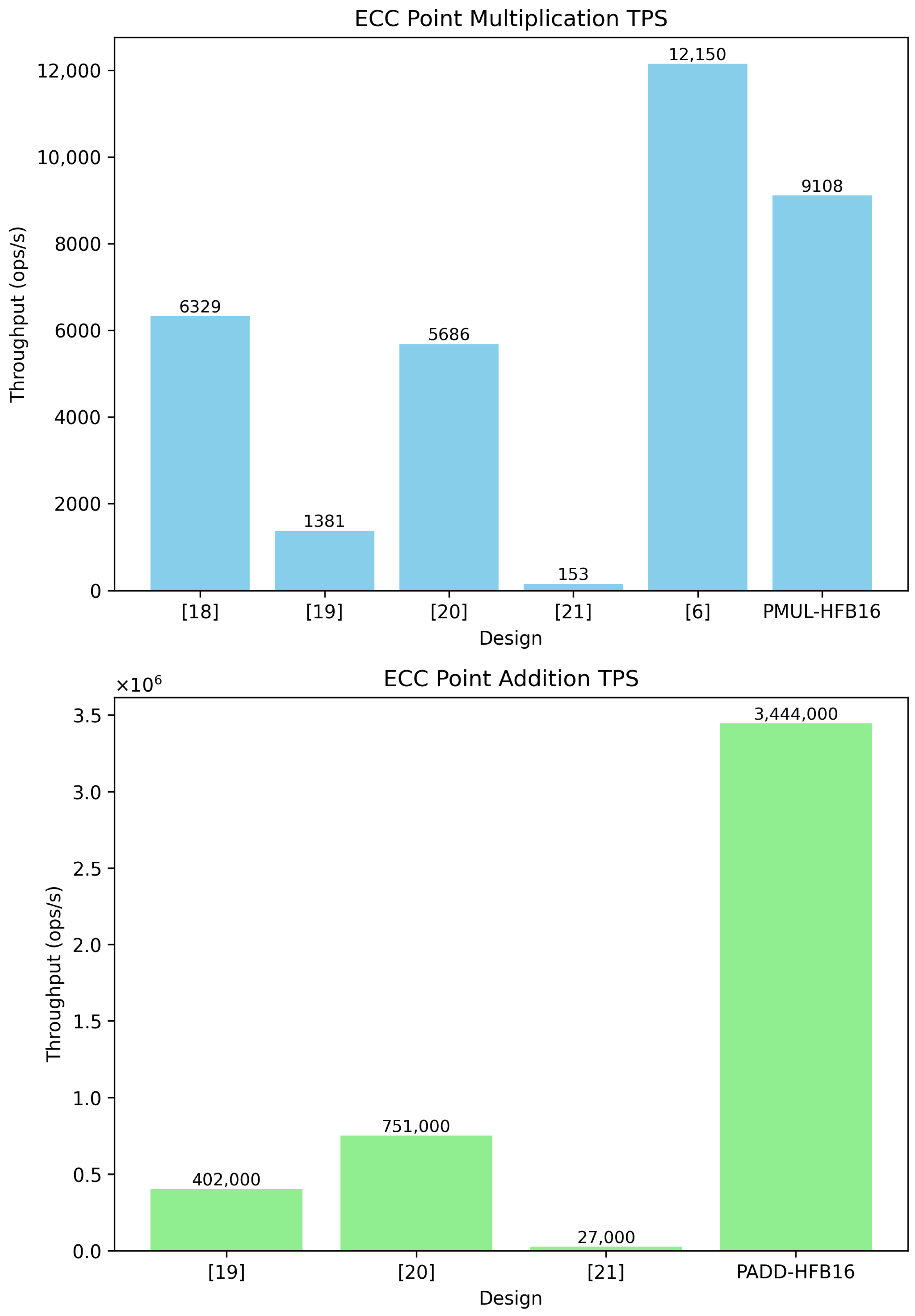
ECC Point Multiplication Comparison
DesignFPGA
Platform
Freq.
(MHz)
AreaTPS
(ops/s)
[18]Virtex-720422,703 LUTs
12,511 FFs
15 BRAMS
136 DSPs
6329
[19]Alveo U250250N/A1381
[20]Virtex
UltrascalePlus
18149,780 LUTs
29,742 FFs
560 DSPs
5686
[21]Statix 107817k ALMs153
[6]Alveo U45N12591,647 LUTs
53,921 FFs
816 DSPs
12,150
PMUL-HFB16
(This work)
Alveo U55C32081,109 LUTs
93,733 FFs
166 BRAMS
288 DSPs
9108
ECC Point Addition comparison
DesignFPGA
Platform
Freq.
(MHz)
AreaTPS
(ops/s)
[19]Alveo U250250N/A0.402   ×   10 6
[20]Virtex
UltrascalePlus
181N/A0.751   ×   10 6
[21]Cyclone V30N/A0.027   ×   10 6
PADD-HFB16
(This work)
Alveo U55C38535,434 LUTs
42,293 FFs
38 BRAMs
144 DSPs
3.444   ×   10 6
Disclaimer/Publisher’s Note: The statements, opinions and data contained in all publications are solely those of the individual author(s) and contributor(s) and not of MDPI and/or the editor(s). MDPI and/or the editor(s) disclaim responsibility for any injury to people or property resulting from any ideas, methods, instructions or products referred to in the content.

