
SimpliFI: Hardware Simulation of Embedded Software Fault Attacks


Abstract
1. Introduction
2. Related Work
2.1. Design Space of Fault Attack Simulation
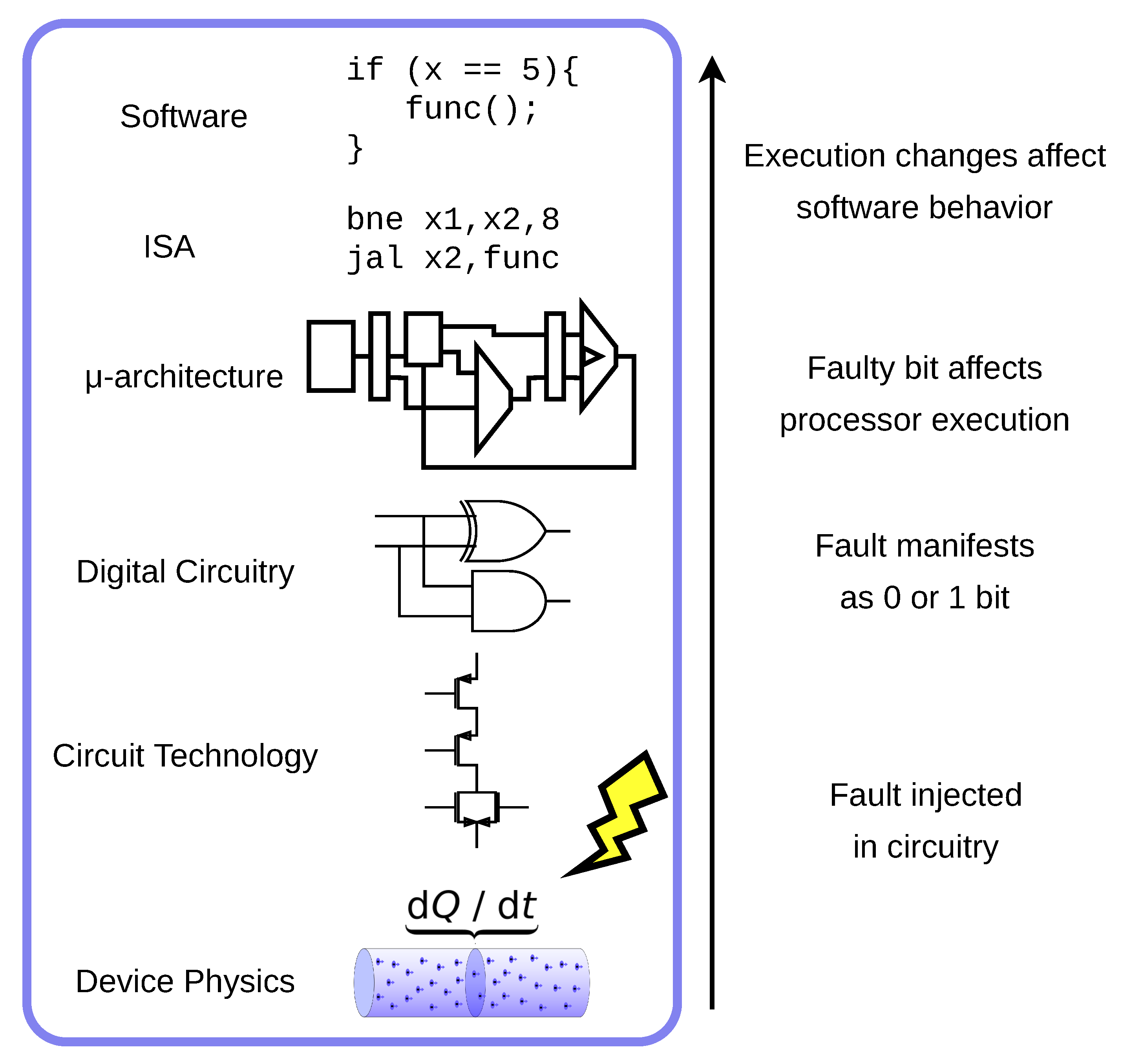
- Fault Injection/Attack—The act of tampering with the system and parameters and environment to cause faults in the hardware.
- Fault Manifestation—The process by which injected faults affect the circuitry and are either successfully incorporated into the hardware state or otherwise lost.
- Hardware Faults/Faulty Bits— The bits in the hardware state that are successfully affected by an injected fault.
- Hardware Fault Propagation—The process by which faulty bits propagate through the hardware, creating erroneous bits in different parts of the circuitry.
- Software Fault—Bits in the software-level state that have been changed by hardware faults. Not every faulty bit in the hardware will have an impact on the correctness of software execution.
- Software Fault Impact/Response—The general changes in software behavior caused by software faults. This may be described quantitatively or qualitatively in terms of instruction execution.
2.2. Fault Characterization of Embedded Software
2.3. Related Work
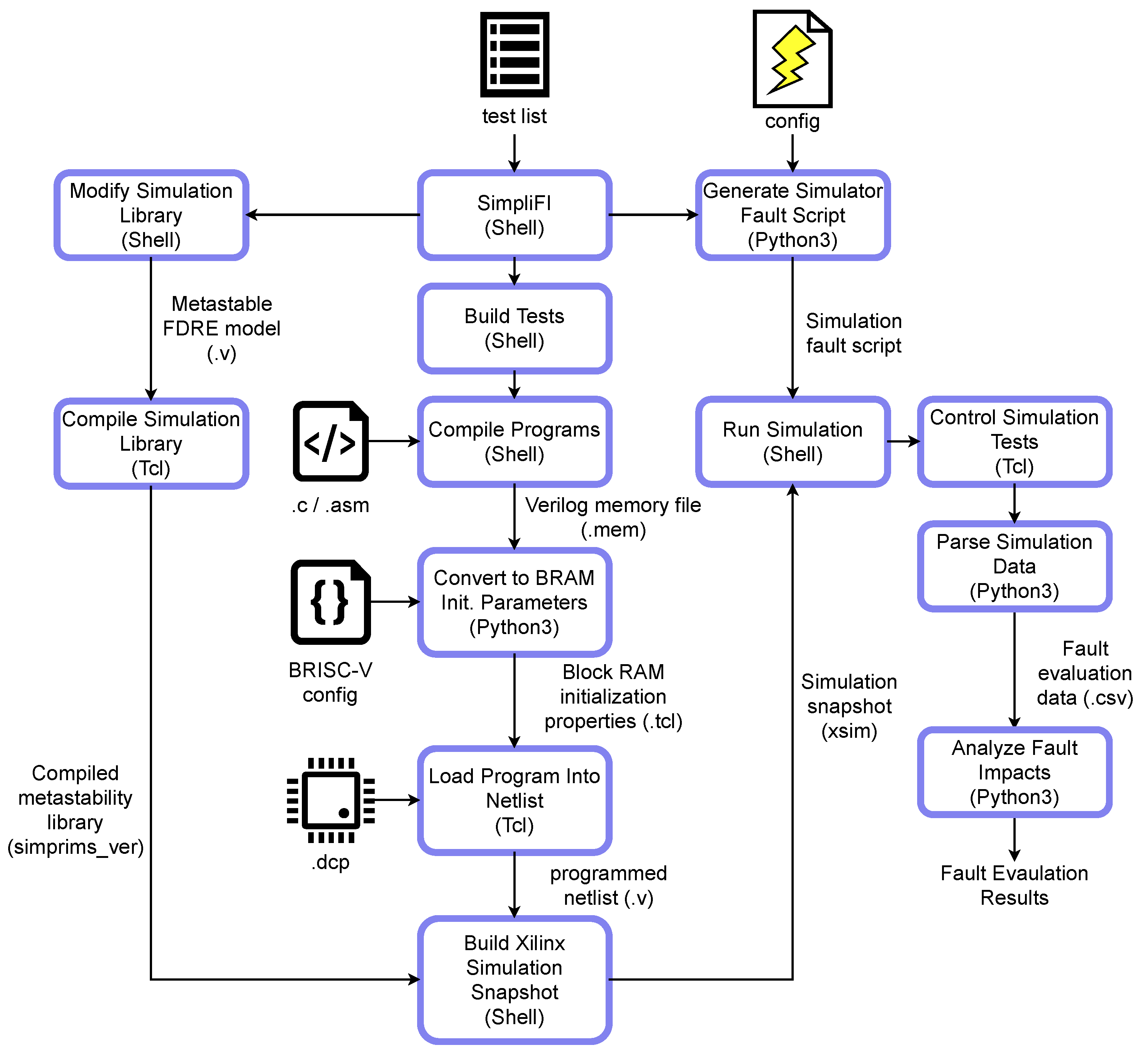
3. Simulation Framework
3.1. Design Space Exploration
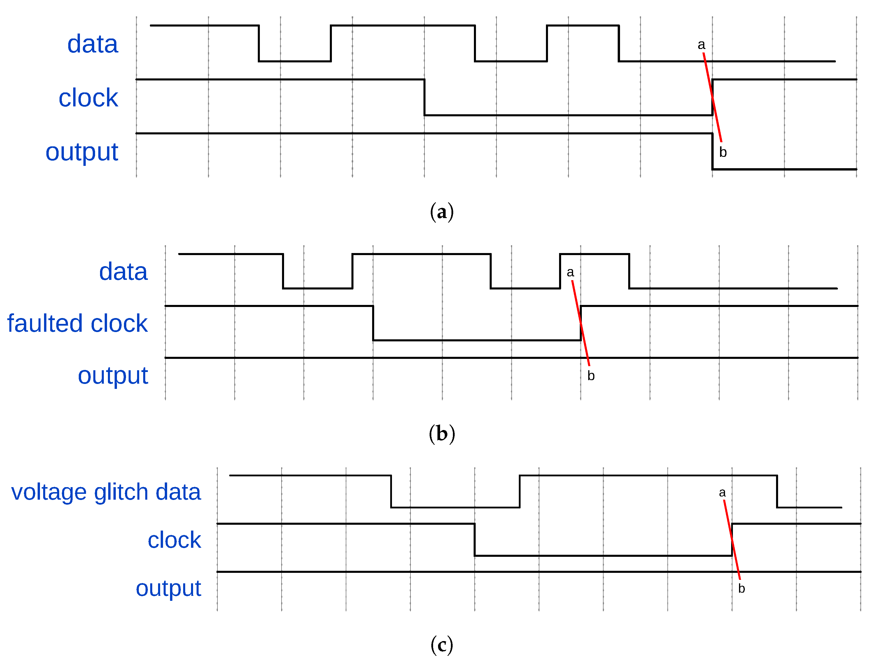
- Simulate Realistic Fault Manifestation—Using a post-layout netlist gives SimpliFI access to physical circuit properties that are critical for modeling realistic fault manifestation. For example, the SDF file of a post-layout netlist can provide device-specific signal propagation delays which enable the framework to model timing-based faults. While VerFI uses a synthesized netlist of device components, the benefit of having hardware-level information is lost by using a software representation of the circuit. Retaining physical information about the device is a key requirement that guarantees that realistic faults are considered during evaluation.
- Capture Hardware Fault Propagation—In order to determine how the simulated faults impact the processor state, hardware-level signals must be tracked so that faulty software-level outcomes can be traced back to corrupted hardware state bits. While physical circuit properties are already required by the fault manifestation design principle, this fault propagation principle requires that the hardware state be actively tracked during execution, and not just during fault injection. An easy way of achieving this is to use gate-level timing simulation with the post-layout netlist, that way signal timing is maintained for design principle 1 and all hardware signals are available and accurate for hardware-level analysis.
- Support Software-Level Analysis—The final results should be tailored towards evaluating software-level behavior. Therefore, SimpliFI implementations must be able to collect software-relevant state at the end of a test, including processor registers, the program counter, and the final processor hardware state. These results should contain at least as much information as what can be collected with physical device testing [11,12]. In conjunction with design principle 2 the software-level data collected by SimpliFI gives users more information than what is possible with physical fault testing methods, where the microarchitectural state is inaccessible.
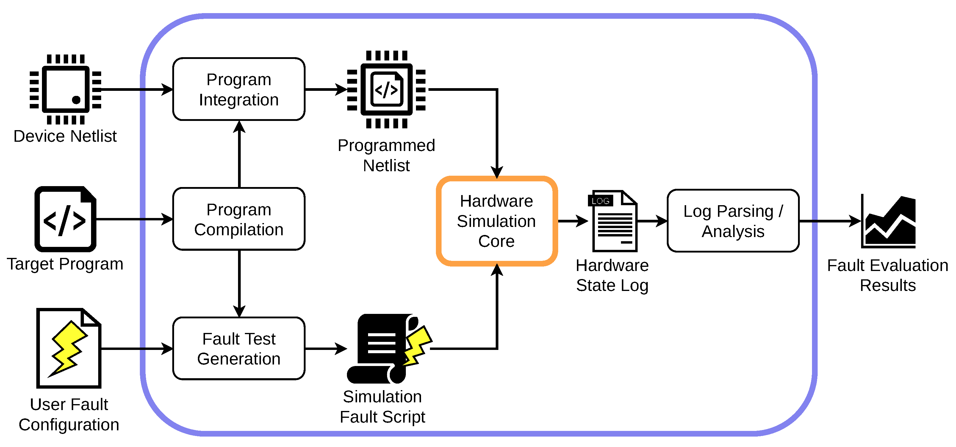
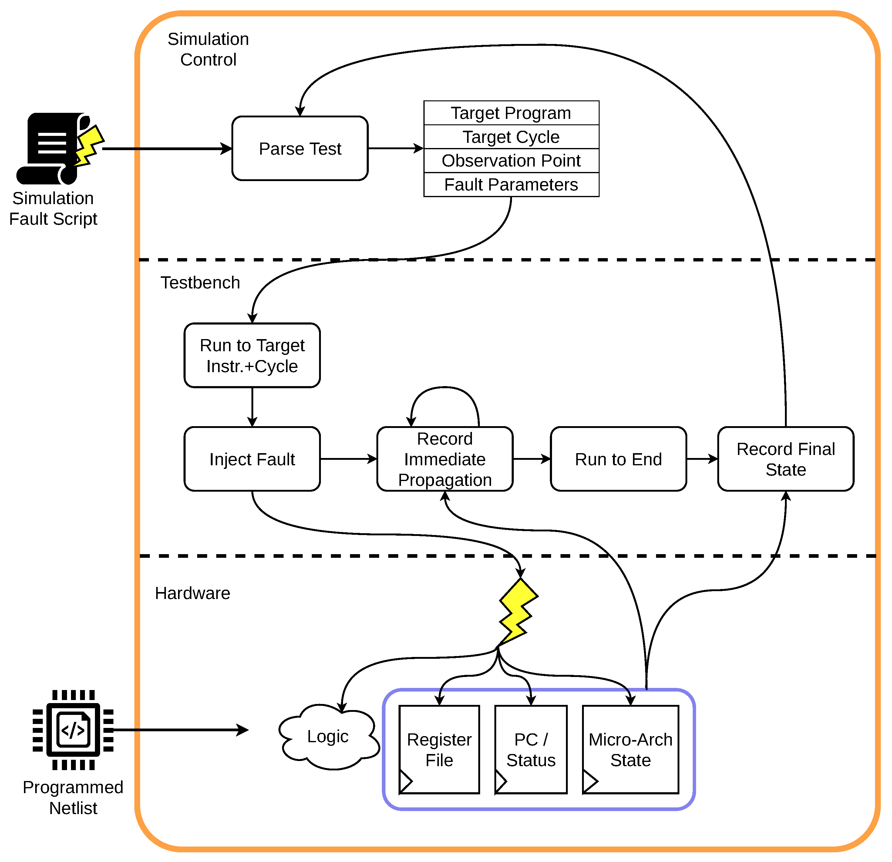
3.1.1. Outer Framework: Software-Centric Control
Test Automation
- Test—A user-defined program and configuration pair that instructs the framework to test different fault injections at multiple points in the target program. A test may encapsulate multiple subtests.
- Subtest—A subtest is one part of a larger test case which specifies a start point, target point, and multiple fault injection trial parameters. The target and start points are described below, and take different meanings when testing instruction sequences vs full applications.
- Fault Injection Trial—A singular execution of the test program with one fault injected during a specific clock cycle.
- Program Type,
- Start Point,
- Target,
- Observe Point,
- Starting Glitch Period,
- Ending Glitch Period, and
- Glitch Period Step.

| SEQ |
| GStep: 0.5 |
| GStart: 12 |
| GEnd: 4 |
| ObservePoint: 7 |
| StartPoint: 2c |
| Target: 0,1,2,3,4,5,6 |
| @@ |
| StartPoint: 4c |
| Target: 0,1,2,3,4,5,6 |
| @@ |
Output Processing
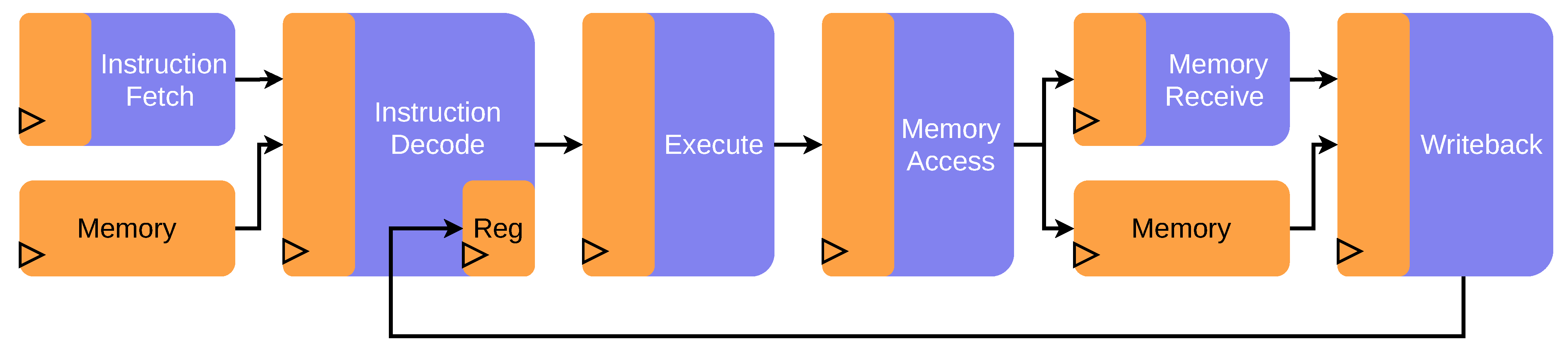
3.1.2. Inner Framework: Hardware Simulation Core
3.2. Fault Modeling
Injection Mechanism Extensions
3.3. Integration in Embedded Flow
4. Results
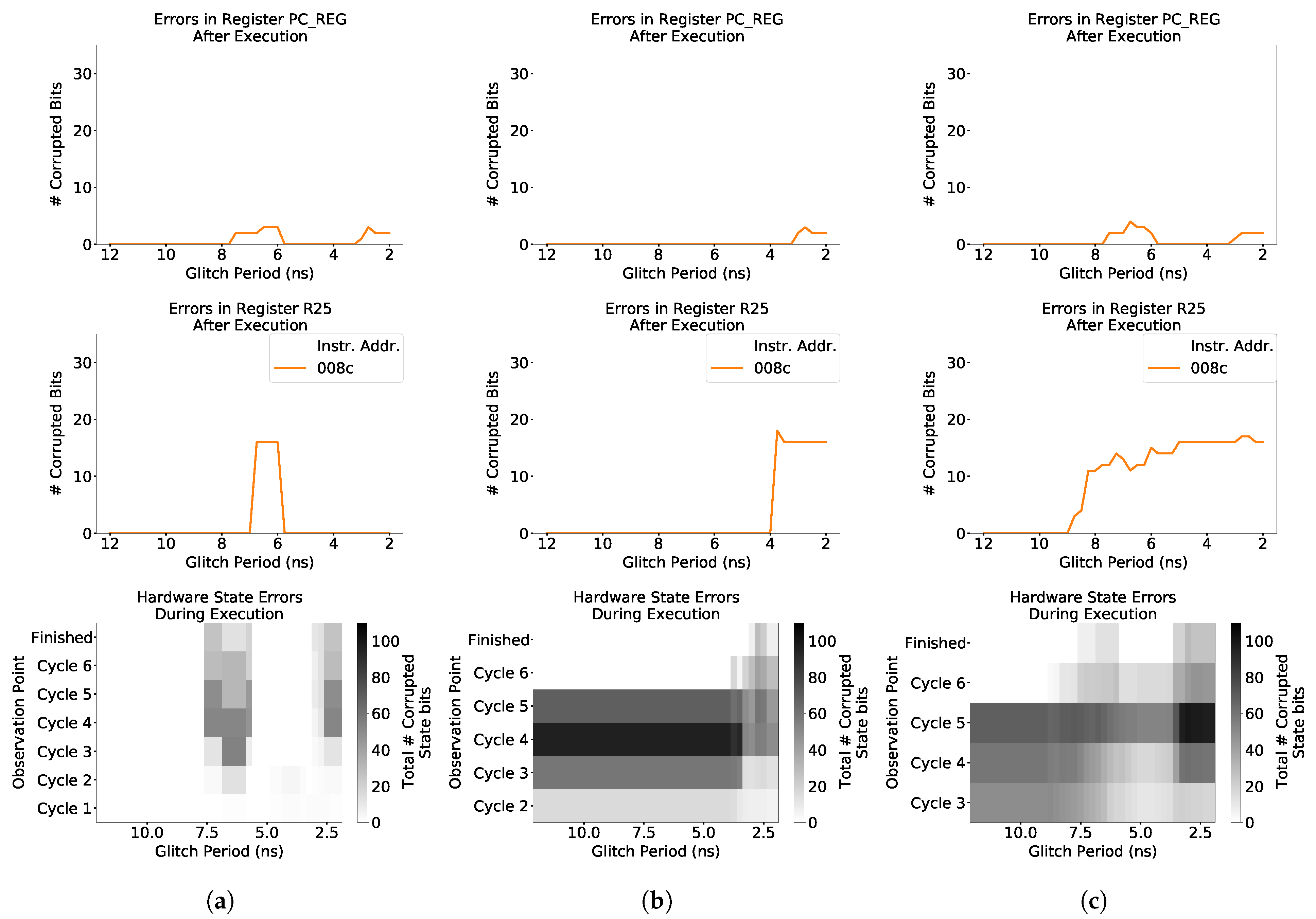
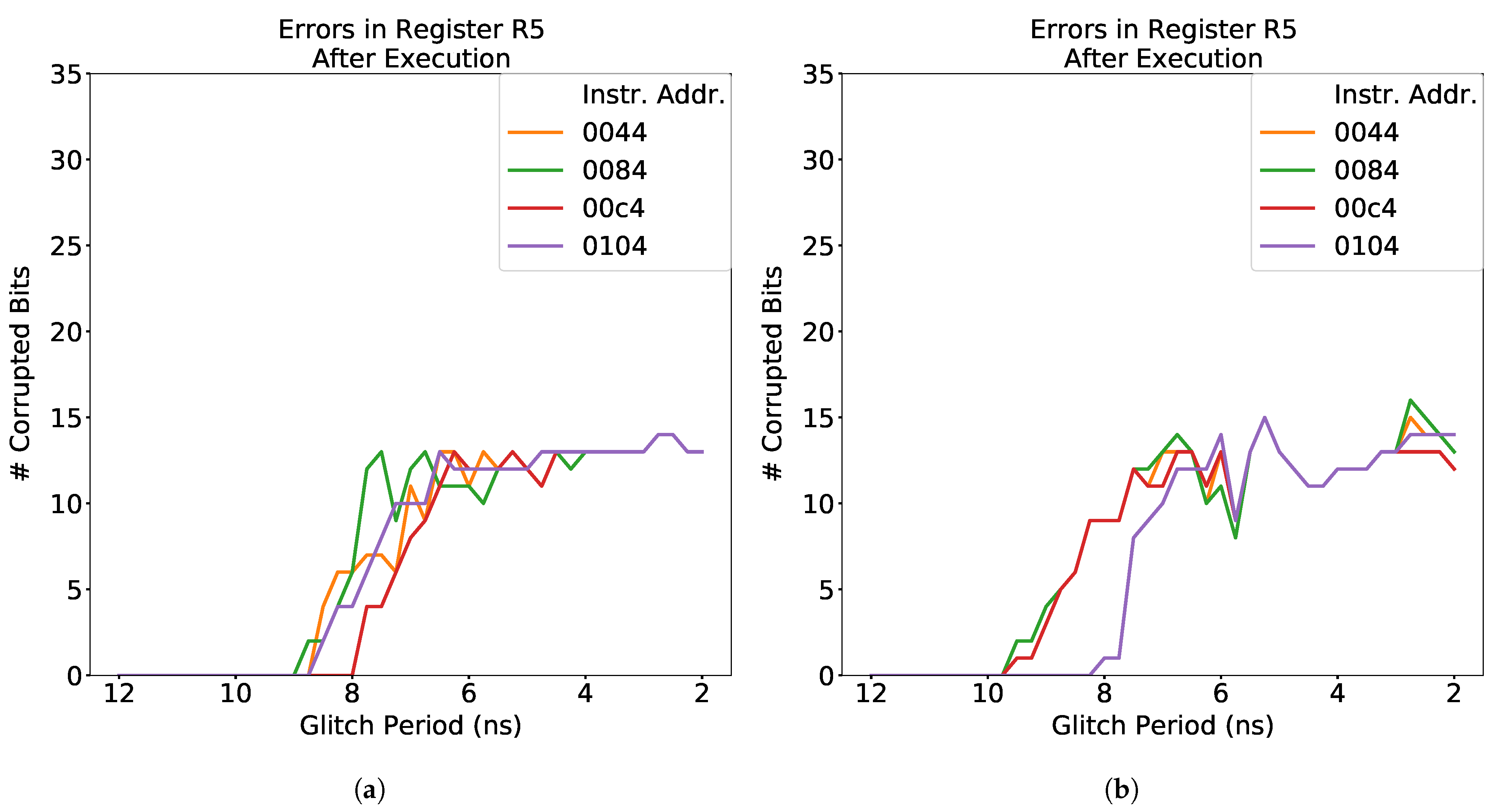
4.1. Characterization at the Instruction Level
- Instruction Component—A portion of the specification for an instruction executed by the processor. Examples of instruction components include the destination register, source registers, and immediate values.
- Instruction Test—A collection of SimpliFI tests that help characterize the behavior of a specific instruction in response to different fault attacks.
- Instruction Component Test—A specific SimpliFI test that is designed to isolate the impact that different microarchitectural blocks have on the instruction fault response by changing one component of the instruction.
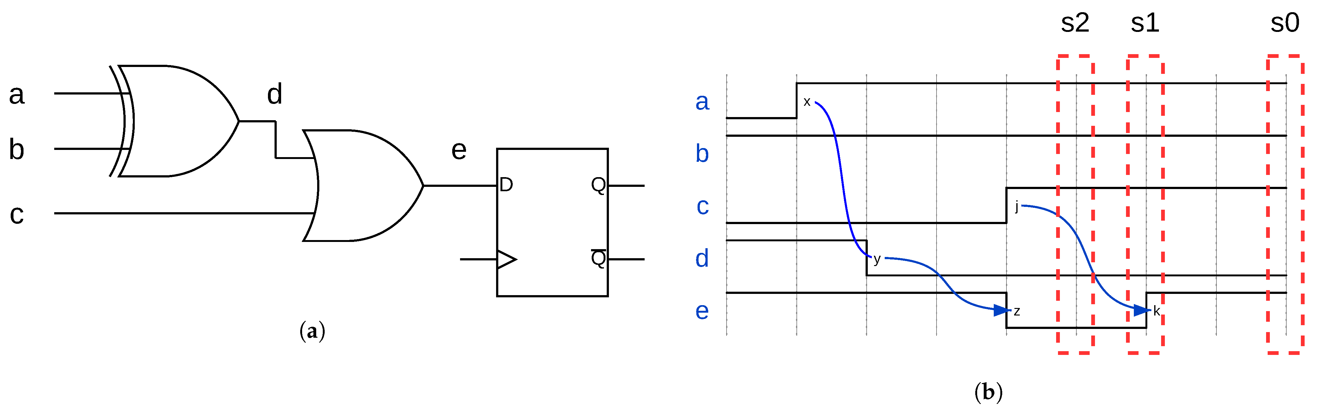
- Fault Response—The behavior of faulty bits in the processor in response to different fault attacks. The results may refer to the fault response of the hardware state as a whole, or of the test outputs. For the test outputs, response is usually qualitatively defined in terms of how the number of faulty output bits changes as a function of the fault injection parameter. For example, a monotonic output response means that, in general, the number of faulty bits in the outputs consistently increases or decreases. An oscillatory output response means that the number of faulty bits alternates between high and low counts as the clock glitch width changes.
- Fault Sensitivity—The range of clock glitch widths which induce erroneous bits in the fault response. This term can apply to both the hardware state fault propagation and the test outputs.
- Fault Intensity—The number of errors induced in the fault response by a fault injection attack. This term can apply to both the hardware state fault propagation and the test outputs.
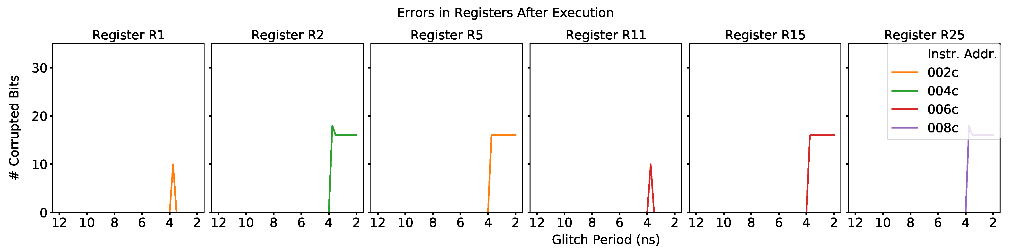
ADD Instruction

LW Instruction
JALR Instruction
Summary
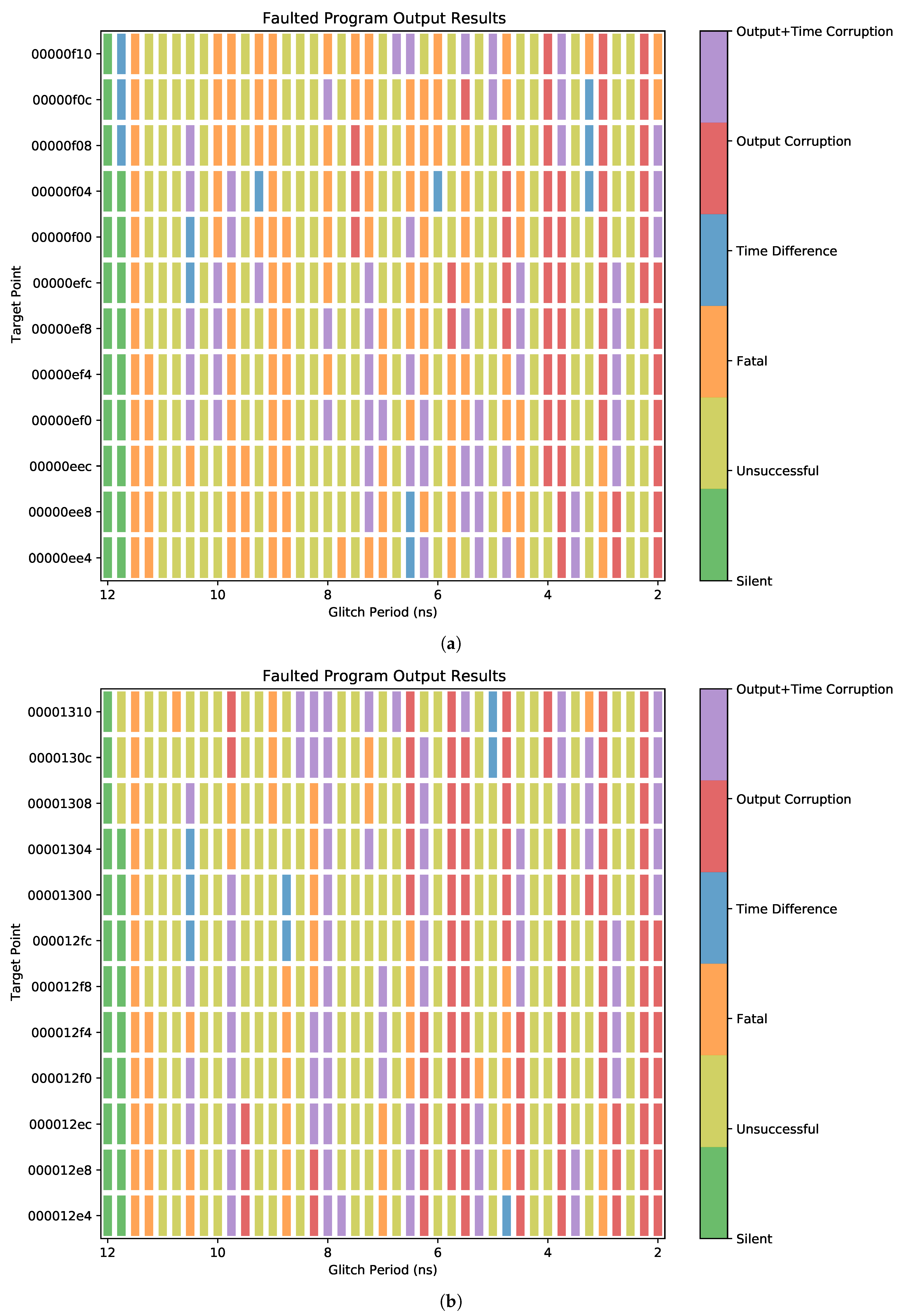
4.2. Characterization at the Application Level
- Unsuccessful Fault—The fault caused no change in program behavior.
- Fatal Error—The program crashed.
- Successful Fault—The program produced faulty outputs.
- Silent Fault—The hardware state was not affected by the fault.
- Unsuccessful Fault—The hardware state was affected, but the fault caused no change in program behavior.
- Fatal Error—The program did not complete within 500 clock cycles beyond the expected execution time.
- Output Corruption—The program produced faulty outputs.
- Time Difference—The program execution time was different than expected, but no outputs were affected.
- Output and Time Corruption—The program both produced faulty outputs and executed in an unexpected number of cycles.
5. Conclusions
Author Contributions
Funding
Data Availability Statement
Conflicts of Interest
Abbreviations
| AES | Advanced Encryption Standard |
| ALU | Arithmetic Logic Unit |
| DFA | Differential Fault Analysis |
| EM | Electromagnetic |
| FPGA | Field-Programmable Gate Array |
| HD | Hamming Distance |
| ISA | Instruction Set Architecture |
| SDF | Standard Delay Format |
References
- Riscure. Riscure FiSim; GitHub: San Francisco, CA, USA, 2020; Available online: https://github.com/Riscure/FiSim (accessed on 1 December 2020).
- Dureuil, L.; Petiot, G.; Potet, M.; Le, T.; Crohen, A.; de Choudens, P. FISSC: A Fault Injection and Simulation Secure Collection. In Proceedings of the Computer Safety, Reliability, and Security—35th International Conference, SAFECOMP 2016, Trondheim, Norway, 21–23 September 2016; Skavhaug, A., Guiochet, J., Bitsch, F., Eds.; Lecture Notes in Computer Science. Springer: Berlin/Heidelberg, Germany, 2016; Volume 9922, pp. 3–11. [Google Scholar] [CrossRef]
- Balasch, J.; Gierlichs, B.; Verbauwhede, I. An In-depth and Black-box Characterization of the Effects of Clock Glitches on 8-bit MCUs. In Proceedings of the 2011 Workshop on Fault Diagnosis and Tolerance in Cryptography, FDTC 2011, Nara, Japan, 29 September 2011; Breveglieri, L., Guilley, S., Koren, I., Naccache, D., Takahashi, J., Eds.; IEEE Computer Society: Los Alamitos, CA, USA, 2011; pp. 105–114. [Google Scholar] [CrossRef]
- van Woudenberg, J.G.J.; Witteman, M.F.; Menarini, F. Practical Optical Fault Injection on Secure Microcontrollers. In Proceedings of the 2011 Workshop on Fault Diagnosis and Tolerance in Cryptography, FDTC 2011, Nara, Japan, 29 September 2011; Breveglieri, L., Guilley, S., Koren, I., Naccache, D., Takahashi, J., Eds.; IEEE Computer Society: Los Alamitos, CA, USA, 2011; pp. 91–99. [Google Scholar] [CrossRef]
- Bandara, S.; Ehret, A.; Kava, D.; Kinsy, M. BRISC-V: An Open-Source Architecture Design Space Exploration Toolbox. In Proceedings of the 27th ACM/SIGDA International Symposium on Field-Programmable Gate Arrays (FPGA), Monterey, CA, USA, 24–26 February 2019; ACM: New York, NY, USA, 2019. [Google Scholar]
- Agrawal, R.; Bandara, S.; Isakov, M.; Mark, M.; Kinsy, M. The BRISC-V Platform: A Practical Teaching Approach for Computer Architecture. In Proceedings of the Workshop on Computer Architecture Education (WCAE), Phoenix, AZ, USA, 22 June 2019. [Google Scholar]
- Bar-El, H.; Choukri, H.; Naccache, D.; Tunstall, M.; Whelan, C. The Sorcerer’s Apprentice Guide to Fault Attacks. Proc. IEEE 2006, 94, 370–382. [Google Scholar] [CrossRef]
- Barenghi, A.; Breveglieri, L.; Koren, I.; Naccache, D. Fault Injection Attacks on Cryptographic Devices: Theory, Practice, and Countermeasures. Proc. IEEE 2012, 100, 3056–3076. [Google Scholar] [CrossRef]
- Yuce, B.; Schaumont, P.; Witteman, M. Fault Attacks on Secure Embedded Software: Threats, Design, and Evaluation. J. Hardw. Syst. Secur. 2018, 2, 111–130. [Google Scholar] [CrossRef]
- Moro, N.; Dehbaoui, A.; Heydemann, K.; Robisson, B.; Encrenaz, E. Electromagnetic Fault Injection: Towards a Fault Model on a 32-bit Microcontroller. In Proceedings of the 2013 Workshop on Fault Diagnosis and Tolerance in Cryptography, FDTC 2013, Santa Barbara, CA, USA, 20 August 2013; Fischer, W., Schmidt, J., Eds.; IEEE Computer Society: Los Alamitos, CA, USA, 2013; pp. 77–88. [Google Scholar] [CrossRef]
- Proy, J.; Heydemann, K.; Berzati, A.; Majéric, F.; Cohen, A. A First ISA-Level Characterization of EM Pulse Effects on Superscalar Microarchitectures: A Secure Software Perspective. In Proceedings of the 14th International Conference on Availability, Reliability and Security, Canterbury, UK, 26–29 August 2019; Association for Computing Machinery: New York, NY, USA, 2019. [Google Scholar] [CrossRef]
- Trouchkine, T. SoC Physical Security Evaluation. Ph.D. Thesis, Université Grenobles Alpes, Grenoble, France, 2016. [Google Scholar]
- Given-Wilson, T.; Jafri, N.; Legay, A. The State of Fault Injection Vulnerability Detection. In Proceedings of the Verification and Evaluation of Computer and Communication Systems—12th International Conference, VECoS 2018, Grenoble, France, 26–28 September 2018; Atig, M.F., Bensalem, S., Bliudze, S., Monsuez, B., Eds.; Lecture Notes in Computer Science. Springer: Cham, Switzerland, 2018; Volume 11181, pp. 3–21. [Google Scholar] [CrossRef]
- Berthier, M.; Bringer, J.; Chabanne, H.; Le, T.H.; Rivière, L.; Servant, V. Idea: Embedded Fault Injection Simulator on Smartcard; Engineering Secure Software and Systems; Jürjens, J., Piessens, F., Bielova, N., Eds.; Springer International Publishing: Cham, Switzerland, 2014; pp. 222–229. [Google Scholar]
- Piscitelli, R.; Bhasin, S.; Regazzoni, F. Fault Attacks, Injection Techniques and Tools for Simulation. In Hardware Security and Trust: Design and Deployment of Integrated Circuits in a Threatened Environment; Sklavos, N., Chaves, R., Di Natale, G., Regazzoni, F., Eds.; Springer International Publishing: Cham, Switzerland, 2017; pp. 27–47. [Google Scholar]
- Yuce, B.; Ghalaty, N.F.; Schaumont, P. TVVF: Estimating the Vulnerability of Hardware Cryptosystems against Timing Violation Attacks. In Proceedings of the 2015 IEEE International Symposium on Hardware Oriented Security and Trust (HOST), Washington, DC, USA, 5–7 May 2015; pp. 72–77. [Google Scholar] [CrossRef]
- Arribas, V.; Wegener, F.; Moradi, A.; Nikova, S. Cryptographic Fault Diagnosis using VerFI. In Proceedings of the 2020 IEEE International Symposium on Hardware Oriented Security and Trust (HOST), San Jose, CA, USA, 7–11 December 2020; pp. 229–240. [Google Scholar]
- Yuce, B.; Ghalaty, N.F.; Deshpande, C.; Santapuri, H.; Patrick, C.; Nazhandali, L.; Schaumont, P. Analyzing the Fault Injection Sensitivity of Secure Embedded Software. ACM Trans. Embed. Comput. Syst. 2017, 16, 1–25. [Google Scholar] [CrossRef]
- Höller, A.; Krieg, A.; Rauter, T.; Iber, J.; Kreiner, C. QEMU-Based Fault Injection for a System-Level Analysis of Software Countermeasures Against Fault Attacks. In Proceedings of the 2015 Euromicro Conference on Digital System Design, DSD 2015, Madeira, Portugal, 26–28 August 2015; IEEE Computer Society: Los Alamitos, CA, USA, 2015; pp. 530–533. [Google Scholar] [CrossRef]
- Ferraretto, D.; Pravadelli, G. Simulation-based Fault Injection with QEMU for Speeding-up Dependability Analysis of Embedded Software. J. Electron. Test. 2016, 32, 43–57. [Google Scholar] [CrossRef]
- Breier, J. On Analyzing Program Behavior under Fault Injection Attacks. In Proceedings of the 11th International Conference on Availability, Reliability and Security, ARES 2016, Salzburg, Austria, 31 August–2 September 2016; IEEE Computer Society: Los Alamitos, CA, USA, 2016; pp. 474–479. [Google Scholar] [CrossRef]
- Xilinx. 7 Series FPGAs Memory Resources; Xilinx Inc.: San Jose, CA, USA, 2019. [Google Scholar]
- Mentor Graphics. ModelSim User’s Manual; Mentor Graphics Corporation: Wilsonville, OR, USA, 2012. [Google Scholar]
- Xilinx. Vivado Design Suite UserGuide: Logic Simulation; Xilinx Inc.: San Jose, CA, USA, 2020. [Google Scholar]
- Gabara, T.J.; Cyr, G.J.; Stroud, C.E. Metastability of CMOS master/slave flip-flops. IEEE Trans. Circuits Syst. II Analog. Digit. Signal Process. 1992, 39, 734–740. [Google Scholar] [CrossRef]
- Horstmann, J.U.; Eichel, H.W.; Coates, R.L. Metastability Behavior of CMOS ASIC flip-flops in Theory and Test. IEEE J. Solid-State Circuits 1989, 24, 146–157. [Google Scholar] [CrossRef]
- Kleeman, L.; Cantoni, A. Metastable Behavior in Digital Systems. IEEE Des. Test Comput. 1987, 4, 4–19. [Google Scholar] [CrossRef]
- Chard, G.F.; Koyuncu, O.; Koh, T.P.R.; Dondershine, S. Modeling Metastability in Circuit Design. U.S. Patent 7139988B2, 10 November 2005. [Google Scholar]
- Dumont, M.; Lisart, M.; Maurine, P. Modeling and Simulating Electromagnetic Fault Injection. IEEE Trans. Comput. Aided Des. Integr. Circuits Syst. 2021, 40, 680–693. [Google Scholar] [CrossRef]
- Blömer, J.; Seifert, J.P. Fault Based Cryptanalysis of the Advanced Encryption Standard (AES). In Financial Cryptography; Wright, R.N., Ed.; Springer: Berlin/Heidelberg, Germany, 2003; pp. 162–181. [Google Scholar]
- Moradi, A.; Shalmani, M.T.M.; Salmasizadeh, M. A Generalized Method of Differential Fault Attack Against AES Cryptosystem. In Proceedings of the Cryptographic Hardware and Embedded Systems—CHES 2006, Yokohama, Japan, 10–13 October 2006; Goubin, L., Matsui, M., Eds.; Springer: Berlin/Heidelberg, Germany, 2006; pp. 91–100. [Google Scholar]
- NIST. Lightweight Cryptography Benchmarking; GitHub: San Francisco, CA, USA, 2021; Available online: https://github.com/usnistgov/Lightweight-Cryptography-Benchmarking (accessed on 24 February 2021).
- Li, Y.; Sakiyama, K.; Gomisawa, S.; Fukunaga, T.; Takahashi, J.; Ohta, K. Fault Sensitivity Analysis. In Proceedings of the Cryptographic Hardware and Embedded Systems, CHES 2010, Santa Barbara, CA, USA, 17–20 August 2020; Mangard, S., Standaert, F.X., Eds.; Springer: Berlin/Heidelberg, Germany, 2010; pp. 320–334. [Google Scholar]


| Method | Injection Methods | Fault Manifestation | HW Propagation | HW Analysis | SW Propagation | SW Analysis |
|---|---|---|---|---|---|---|
| TVVF [16] | ⊚ | • | • | • | ∘ | ∘ |
| VerFI + Modeling [17] | • | ∘ | • | • | ∘ | ∘ |
| MAFIA [18] | ⊚ | • | ⊚ | ⊚ | ∘ | ⊚ |
| FiSim [1] | ∘ | ∘ | ∘ | ∘ | • | • |
| SimpliFI (this) | ⊚ | • | • | • | ⊚ | • |
| Instruction | Corrupted Output In... | Target Stage | ||||||
|---|---|---|---|---|---|---|---|---|
| 0 | 1 | 2 | 3 | 4 | 5 | 6 | ||
| ADD | Intended Reg | √ | √ | √ | √ | √ | ||
| Other Reg | √ | |||||||
| LW | Intended Reg | √ | √ | √ | √ | √ | √ | |
| Other Reg | √ | √ | ||||||
| JALR | Intended Reg | √ | √ | √ | √ | √ | ||
| Other Reg | √ | |||||||
| Instruction | Component | Target Stage | ||||||
|---|---|---|---|---|---|---|---|---|
| 0 | 1 | 2 | 3 | 4 | 5 | 6 | ||
| ADD | Destination | • | ∘ | ∘ | ||||
| Source 1 | • | |||||||
| Source 2 | ∘ | • | ∘ | |||||
| LW | Destination | • | • | ∘ | ||||
| Source | • | |||||||
| Immediate | ∘ | • | ∘ | ∘ | ∘ | |||
| JALR | Destination | • | ∘ | |||||
| Source | ∘ | ∘ | ∘ | |||||
| Immediate | ∘ | |||||||
| Location | % of Total Test Outcomes | |||||
|---|---|---|---|---|---|---|
| Silent | Unsuccessful | Fatal | Time Difference | Output Corruption | Output+Time Corruption | |
| Round 1 | 4.27 | 45.12 | 25.40 | 2.44 | 10.98 | 11.79 |
| Round 9 | 4.27 | 49.19 | 11.38 | 1.63 | 18.90 | 14.63 |
Publisher’s Note: MDPI stays neutral with regard to jurisdictional claims in published maps and institutional affiliations. |
© 2021 by the authors. Licensee MDPI, Basel, Switzerland. This article is an open access article distributed under the terms and conditions of the Creative Commons Attribution (CC BY) license (https://creativecommons.org/licenses/by/4.0/).
Share and Cite
Grycel, J.; Schaumont, P. SimpliFI: Hardware Simulation of Embedded Software Fault Attacks. Cryptography 2021, 5, 15. https://doi.org/10.3390/cryptography5020015
Grycel J, Schaumont P. SimpliFI: Hardware Simulation of Embedded Software Fault Attacks. Cryptography. 2021; 5(2):15. https://doi.org/10.3390/cryptography5020015
Chicago/Turabian StyleGrycel, Jacob, and Patrick Schaumont. 2021. "SimpliFI: Hardware Simulation of Embedded Software Fault Attacks" Cryptography 5, no. 2: 15. https://doi.org/10.3390/cryptography5020015
APA StyleGrycel, J., & Schaumont, P. (2021). SimpliFI: Hardware Simulation of Embedded Software Fault Attacks. Cryptography, 5(2), 15. https://doi.org/10.3390/cryptography5020015