Article

Determination of the Contact Resistance of Planar Contacts: Electrically Conductive Adhesives in Battery Cell Connections

1
Chair of Electrical Energy Storage Technology (EES), Department of Energy and Process Engineering, TUM School of Engineering and Design, Technical University of Munich (TUM), Arcisstr. 21, 80333 Munich, Germany
2
Institute for Machine Tools and Industrial Management (iwb), Department of Mechanical Engineering, TUM School of Engineering and Design, Technical University of Munich (TUM), Boltzmannstr. 15, 85748 Garching, Germany
*
Author to whom correspondence should be addressed.
Batteries 2023, 9(9), 443; https://doi.org/10.3390/batteries9090443
Submission received: 1 August 2023 / Revised: 23 August 2023 / Accepted: 26 August 2023 / Published: 29 August 2023
(This article belongs to the Section Battery Modelling, Simulation, Management and Application)

Abstract

:
This study presents a method to analyze the electrical resistance of planar contacts. The method can determine whether the contact resistance of the joint exhibits linear or non-linear behavior. By analyzing the current distribution over a planar contact, it can be determined whether an area-based contact resistance is justified or if other parameters define the contact resistance. Additionally, a quantitative evaluation of the factors that affect the measurement accuracy, including the positioning, the measurement equipment used, and the influence of the current injection on the sense pin was conducted. Based on these findings, the electrical contact resistance and the mechanical ultimate tensile force of a silver-filled epoxy-based adhesive are analyzed and discussed. The layer thickness and the lap joint length were varied. Overall, the investigated adhesive shows a low contact resistance and high mechanical strength of the same magnitude as that of well-established joining techniques, such as welding, press connections, and soldering. In addition to evaluating the mechanical and electrical properties, the electric conductive adhesive underwent an economic assessment. This analysis revealed that the material costs of the adhesive significantly contribute to the overall connection costs. Consequently, the effective costs in mass production are higher than those associated with laser beam welding.

1. Introduction

Electrical connections are necessary for many mobile and stationary applications to connect lithium-ion batteries to an electrical load or charger. In addition to providing high mechanical strength, minimizing the electrical resistance is one of the most critical challenges in contacting lithium-ion batteries for electric vehicle (EV) powertrains and for stationary energy storage [1,2,3,4]. Depending on the application, individual target parameters must be optimized. Such parameters can include the maximum heat input during joining or cost. In order to manufacture electrical connections, a variety of joining techniques are commonly used. For instance, Das et al. [1] conducted a comprehensive review of joining techniques for battery packs, providing insights into resistance spot welding, laser beam welding, ultrasonic welding, soldering, and mechanical assembly techniques. Reichel et al. [5] investigated the joining for a hybrid busbar made of copper and aluminum using a forming process. Clamped cell connectors and their effect on the electrical contact resistance was investigated by Bolsinger et al. [6]. Brand et al. [2,3,4] assessed the contact resistance ( R C ) and ultimate tensile force (UTF) of welded, soldered, and press-contacted battery packs. Additionally, Wassiliadis et al. [7] investigated the influence of electrical contact resistance on lithium-ion battery testing for fast-charge applications.
Functional adhesives are an alternative to these well-established contacting techniques. They are generally defined as adhesives that fulfill a role beyond the adhesive’s primary function of creating a mechanical bond between two substrates. They are typically thermally conductive adhesives (TCA) or electrically conductive adhesives (ECA). Due to their low processing temperatures, their ability to join dissimilar materials, and their reduced complexity for processing, ECA may have the potential as an alternative to currently widespread joining processes regarding R C and UTF [8].
This paper aims to analyze the viability of functional adhesives for creating electrically conductive connections, with a particular emphasis on the current distribution in planar (area-based) contact resistances. Furthermore, this paper highlights the importance of quantifying and minimizing influencing factors of the measurement setup to achieve precise and reproducible results. Based on these findings, an ECA is quantitatively evaluated by geometrically simplified samples and compared to well-established joining techniques. The research objectives of this work are summarized as follows:
  • How does the setup influence the contact resistance measurement accuracy?
  • How can the contact resistance be determined as a function of the contact area?
  • How do the electrical and mechanical properties of the investigated ECA differ from those of welding, soldering, and press contacts as shown by Brand et al. [2,3,4]?
In this paper, planar contact refers to an electrical connection between two surfaces. The relationship between contact area and resistance is defined as an area-based quantity.

Electrical Joining Techniques

Welding is a vital joining technique for EV powertrains because it can provide mechanically robust electrical connections with low resistances [2]. Applicable welding techniques for battery applications include resistance spot welding, ultrasonic welding, and laser beam welding. Resistance spot welding generates a weld seam by passing a current from two electrodes through the joined components, rapidly heating the contact surface and melting the joining partners. It is best-suited for applications that require relatively thin connections. During the ultrasonic welding process, ultrasonic vibrations lead to the objects being scrubbed into each other until they are joined together. An advantage of this process is that the metal surface is exposed to the induced vibrations, which remove oxides and contaminants from the welding surface [9]. Furthermore, low process temperatures are needed for ultrasonic welding, which provide a significant benefit to weld battery terminals [2]. In addition, dissimilar materials can be joined using ultrasonic welding [10,11]. However, the joining components can be damaged during this process when materials with high hardness are used [2,9,12]. Laser beam welding uses laser radiation, which melts the joining components with a very precise weld seam at high welding speeds [13]. By adapting the weld seam trajectory [14], the temporal [15] or spatial [16] power distribution, or the wavelength of the laser radiation [17], a broad range of materials with varying thicknesses and desired weld seam properties can be joined.
Besides welding processes, electrical connections can also be manufactured by mechanical assembly. Press contacts and screwed joints provide a detachable alternative to welding and establish contacts by direct mechanical contact of the current-carrying members. Detachable joining techniques are desirable because of their repairability and ease of manufacturing, contributing to more sustainable EV powertrain systems and reducing the level of training required for personnel in manufacturing facilities [18]. Due to the repairability enabled by press contacts, this joining method is suitable for creating electrical connections at the battery-pack level. In addition, mechanical assembly typically does not require any heat input during manufacturing, further increasing the appeal of detachable contacts for battery assemblies and systems containing heat-sensitive electrical components [3,18].
Finally, soldering represents another joining technique. An additional material is melted into the joint by applying heat [19,20]. This third material is referred to as solder. Soldering is commonly applied in microelectronics applications and represents a proven process for creating connections between dissimilar materials [1]. Soldering has limited suitability for temperature-sensitive applications, such as lithium-ion batteries, as heat is necessary for this process to melt the solder.
A general comparison between welding, press contacts, and soldering concerning their electrical and mechanical performance was conducted by Brand et al. [2,3,4]. In their studies, contact resistance ( R C ) and UTF were assessed as representative quantities for electrical and mechanical performance.

2. Basics of Electrically Conductive Adhesives

As defined in DIN EN 923, an adhesive is a non-metallic substance connecting two materials via surface adhesion. A sufficiently strong bond between the materials is created and maintained through cohesion [21]. Adhesives are polymeric materials composed of hydrocarbon-based monomer units that combine to form long polymer chains with a high degree of interconnection.
ECAs are composite materials comprised of a polymer adhesive matrix and electrically conductive fillers. Figure 1a shows a schematic of an isotropically conductive adhesive (ICA) joint cross section with a polymer binder, electrically conductive flakes, and resulting electrical conduction between two specimens. The resistances mentioned are categorized as follows: R A and R B represent the resistances of the specimens along the length of the lap joint, R L denotes the resistance of the layer, and R S 1 and R S 2 represent the resistances of the surfaces. The combined sum of these resistances is defined as the lap joint resistance, denoted as R LJ . According to Holm [22], the contact resistance ( R C ) is defined as the sum of film or layer resistance ( R L ), and the resistances of the surfaces ( R S 1 and R S 2 ) where the electrical conduction takes place within a-spots. While the polymer matrix provides the ECA with its mechanical properties, the conductive filler is responsible for enabling the electrical conductivity of the ECA [23,24]. In order to better understand how adhesives become electrically conductive, it is necessary to refer to the percolation theory of conduction [23]. Based on this theory, the conductivity of the ECA remains constant at low filler concentrations, providing only minimal conductivity of the bulk material. However, once the percolation threshold, as indicated by the vertical dashed line in Figure 1b, is reached, the conductivity increases dramatically. Increasing the filler material content beyond the percolation threshold typically yields diminishing returns and can lead to worse mechanical properties of the ECA [23]. The percolation threshold typically occurs at a volume fraction of 15–25%, although this value is dependent on the size and shape of the flakes [23]. Due to this behavior, ECAs can be categorized based on their placement within the graph shown in Figure 1b, where anisotropically conductive adhesive (ACA) and ICA represent the dominant categories of ECA. In contrast to ACAs and ICAs, non-conductive adhesives (NCAs) do not contain conductive fillers but provide a direct mechanical bond between contacting surfaces instead.
ACAs differ from ICAs in the direction of their conductive properties. While ACAs only conduct electricity in one direction, ICAs conduct electricity in all three dimensional directions. Below the percolation threshold, electricity cannot be conducted throughout the polymer matrix due to the low filler content. Above the percolation threshold, however, the filler particles create a three-dimensional conductive network, forming an ICA [23,25].
Besides the conductivity, another drawback of the application of an ACA is that heat and pressure are required during the curing process to ensure proper contact [23]. An ICA, however, does not necessarily require heat and pressure to form an adequate electrical contact. Depending on the properties of the polymer matrix of the ICA, the adhesive can be cured at room temperature, and the process can be accelerated by applying higher temperatures. For example, the silver-filled epoxy-based ICA from Polytec PT GmbH (PT EC 244) has a curing time of 24 h at room temperature, while curing can also occur in 15 min at 80 C . This property of ICAs provides a significant advantage in scenarios where high-temperature curing is not feasible or desired. In the past, studies of ECA as an alternative to soldering in microelectronics were published, [24,25,26,27,28,29,30]. The present study, on the other hand, deals with high-current applications, which are also found in battery systems. Measurements are used to verify whether an area-based contact resistance is justified or whether other parameters determine the contact resistance. These findings can be applied to all contact techniques and to the design and optimization of contact connections. Additionally, R C and UTF are compared with well-established joining techniques, such as welding, press connections, and soldering.

3. Experimental

Based on the studies of Brand et al. [2,3,4], two rectangular specimens, denoted as A and B and forming a lap joint, were investigated. Each specimen had dimensions of 50 mm × 15 mm and a lap joint length ( l LJ ) with another specimen across a l LJ × 15 mm area. The adhesive layer thickness between the two specimens is defined by h L . In comparison to Brand et al. [2,3,4], the sample thickness of the brass samples was increased to 2 mm to achieve a better measurement of the contact resistance ratio. Furthermore, four sense pins were used on each specimen, denoted as A m = 1 4 and B n = 1 4 . Figure 2a shows the sample layout. In order to achieve defined testing conditions between the two specimens, the layer thickness ( h L ) was varied between 38, 89, and 124 µ m , and the layer length ( l LJ ) was varied between 5, 10, and 15 mm. Spacer particles in the above defined layer thicknesses from Rock West Composites Inc. were used. In a preliminary study, several adhesives were examined. These included PC 3001 from Heraeus and EC 262 and EC 244 from Polytec PT GmbH. EC 262 exhibited excessive resistance and was excluded from further investigations in this study. EC 244 and PC 3001 both showed very low contact resistance and high mechanical strength. However, PC 3001 was unsuitable for battery applications because it requires a curing temperature above 120 C . Therefore, the silver-filled epoxy-based isotropically and electrically conductive adhesive from Polytec PT GmbH (PT EC 244) was used for all investigations reported in this paper.

3.1. Measurement of Electrical Contact Resistance

For an accurate and reproducible measurement, the influence of the measurement equipment, the positions of the sense pins, and the presence of inhomogeneities on the measurement must be known.
Therefore, measurements were carried out using an electrical contact tester developed by Li.plus GmbH based on the four-wire measurement principle. Each measurement contained a pulse series of five pulses, with a pulse duration of 25 ms. The two power and sense lines were twisted separately from to minimize electromagnetic interference. A current of 5 A was applied to the power lines, and the voltage was measured with the sense lines. In order to minimize position inconsistencies, a custom-made test fixture including gold-plated spring-loaded contact pins with a continuous plunger by Feinmetall GmbH was used, based on the geometry shown in Figure 2a and Figure A1. This fixture contained two power pins to apply the measurement current ( ± I tot ) and eight sense pins on both specimens, denoted by the subscripts A m = 1 4 and B n = 1 4 , to measure the potential distribution between every combination of measurement pins ( U Am , Bn ). Therefore, all measurements had identical distances between the sense and power pins. With this high amount of sense points, position inconsistencies can be minimized, and the specific resistance of both specimens can be determined (see Section 3.1.3 Performing the Measurement). Furthermore, the measurements were performed automatically via a multiplexer (MUX).
As part of this experiment, the capability of the measurement process is proven according to the standards specified in German Association of the Automotive Industry (VDA) Volume 5. The accuracy of the contact tester without recontacting the power and sense pins was identified to a standard deviation of less than 3.634 · 10 9   Ω at an expected value of 70.47 · 10 6   Ω over 25 measurements. An additional influencing factor is the recontacting of the measurement pins to the same sample. Throughout 25 recontacting measurements, a standard deviation of less than 26.29 · 10 9   Ω was determined. This corresponds to a relative standard deviation of less than 0.0373%. With this measurement quality, the contact resistance in the expected order of magnitude of 1 · 10 5 to 1 · 10 3   Ω can be reliably measured and analyzed. Hence, the commercial electrical contact tester developed by Li.plus GmbH was suitable. However, other electrical contact testers could also be employed, provided they demonstrate the same level of accuracy. Furthermore, at least five test samples were tested and averaged to achieve high accuracy and certainty.
Additionally, a simulation based on on finite element method (FEM) was carried out to verify the influences of the measurement setup. Based on the experimental investigations, a model of a sample was implemented in COMSOL Multiphysics. The modeled brass sample ( σ b r a s s A , B = 15.5 · 10 6 S/m) consisted of a contact area of 15 mm × 15 mm, a homogeneous surface resistance of 2.25 · 10 8   Ω m 2 , and a third layer ( σ L = 2 · 10 5 S/m), which represents ECA. A current of 5 A across the surface ( ± I tot ) was applied. The ground potential of the simulation was set to the top of the negative power pin, which was modeled as a cylinder with a height of 0.1 mm and a radius of 0.1 mm. The specific surface resistance of the power pins was set to 675 · 10 18   Ω m 2 , and that of the layer was set to 2.25 · 10 8   Ω m 2 . The objective of the simulation was to demonstrate the effects of the measurement setup rather than to parameterize it based on the measurement outcomes.
All materials and contact conditions were assumed to be homogeneous and isotropic. The resulting voltage drop across x = 7.5   mm over y and the positions of the sense pins ( A m and B n ), as well as the current injection ( ± I tot ) are illustrated in Figure 2b. The voltage curve over y in Figure 2b shows two peaks. The first appears at the current injection at ± I tot , and the second appears around the contact area.

3.1.1. Phenomena at the Current Injection

The voltage peaks near the current injection point ( I tot ) are now considered. Around this point, x = 7.5   mm and y = 2   mm , a radially symmetrical equipotential field is formed. Figure 3a illustrates the equipotential lines on the sample’s surface. The equipotential lines change from radially symmetrical to linear behavior as the distance from the point of current impingement increases (in the y direction in this case). An infinitely large surface is considered for the theoretical view of this phenomenon. As discussed by Prechtl [31], when a current is injected at any point on an infinitely large surface, an electric field with radially symmetrical behavior results. Therefore, the radially symmetrical behavior of the equipotential lines never ends. The resulting potential ( ϕ ) depends on the specific resistance ( ρ ), the injected current (I), and the radial distance (r), as illustrated in Equation (1) [31].
ϕ = ρ I 2 π r
If one dimension is finite, this behavior cannot be observed. Figure 3b represents the resulting potential from the FEM simulation along the y axis at x = 7.5   mm . For a comparison with linear behavior, according to Equation (2), the linear drop of the potential is depicted in Figure 3b.
R = ρ l A
The greater the distance from the current impingement point (see Figure 3b), the closer the potential approaches the linear function. If the relative error is considered, as shown in Figure 3c, it is evident that this behavior of the potential is independent of the specific resistance of the investigated material but depends on the geometry of the specimen. An analogy was found in mechanics with the principle of Saint Venant. The principle of Saint Venant states that the inhomogeneity caused by a load on a long cuboid depends on its geometry. After a distance of at least half the longest side length of the specimen’s cross-sectional area (A; variable t in Figure 2a), the magnitude of the inhomogeneity is negligible, and the behavior becomes linear [32,33]. The same results are represented in Figure 3b. A mathematical analysis of the decaying behavior of the inhomogeneity is provided within Poisson’s equation in Appendix C.1. The analytical equation represents how inhomogeneity influences the voltage curve concerning the geometrical dimensions (see Equation (A8)). The Transmission line model proposed by Murrmann and Widmann [34], as well as Berger [35], can demonstrate a similar phenomenon when modeling semiconductors.
In summary, special attention must be paid to this influence when determining geometrical and electrical quantities. The linear equation of the resistance calculation according to the length (l), area (A), and specific resistance ( ρ ) (Equation (2)) can therefore only be used if the assumption is made that the material to be investigated is homogeneous and isotropic. Furthermore, the geometrical parameters of the sample are finite, and the measurement must be taken at a sufficient distance from the point of a current impingement.
The distance of the voltage measurement to the current injection point is essential to determine and compare the electrical contact resistance. Considering the impact of voltage distribution during current injection, it is advisable to maintain a minimum distance between power and sense points equivalent to half the longest side length of the cross-sectional area (A) of the specimen. This helps to minimize the error resulting from contacting below 0.05%, as illustrated in Figure 3c. Therefore, the measurements were carried out in the linear area to optimize the measurement results.
In order to compare samples to each other, a smaller distance between the power and sense pins can be chosen. As the distance to the point of current impingement decreases, as shown in Figure 3c, the local derivative of the voltage increases. However, special attention must be paid to the positioning of the voltage measurement. The closer the voltage measurement is located to the current impingement point, the greater the effect of a position inaccuracy on the measurement accuracy. The area of the power pin defines the maximum voltage peak at the current injection point. A thinner power pin results in a higher voltage peak. In contrast, a large homogeneous area-based current injection results in a lower voltage peak.
Another factor that must be considered to determine the contact resistance is the ratio between the contact resistance and the measured total resistance, which should be close to 1. If the ratio is too small, slight variations in the geometry, material, and positioning of the measurement pins can significantly impact the quality of the measurement. In order to keep the quality of the results high, thicknesses of 2 mm and 0.2 mm were chosen for the brass and copper samples, respectively.

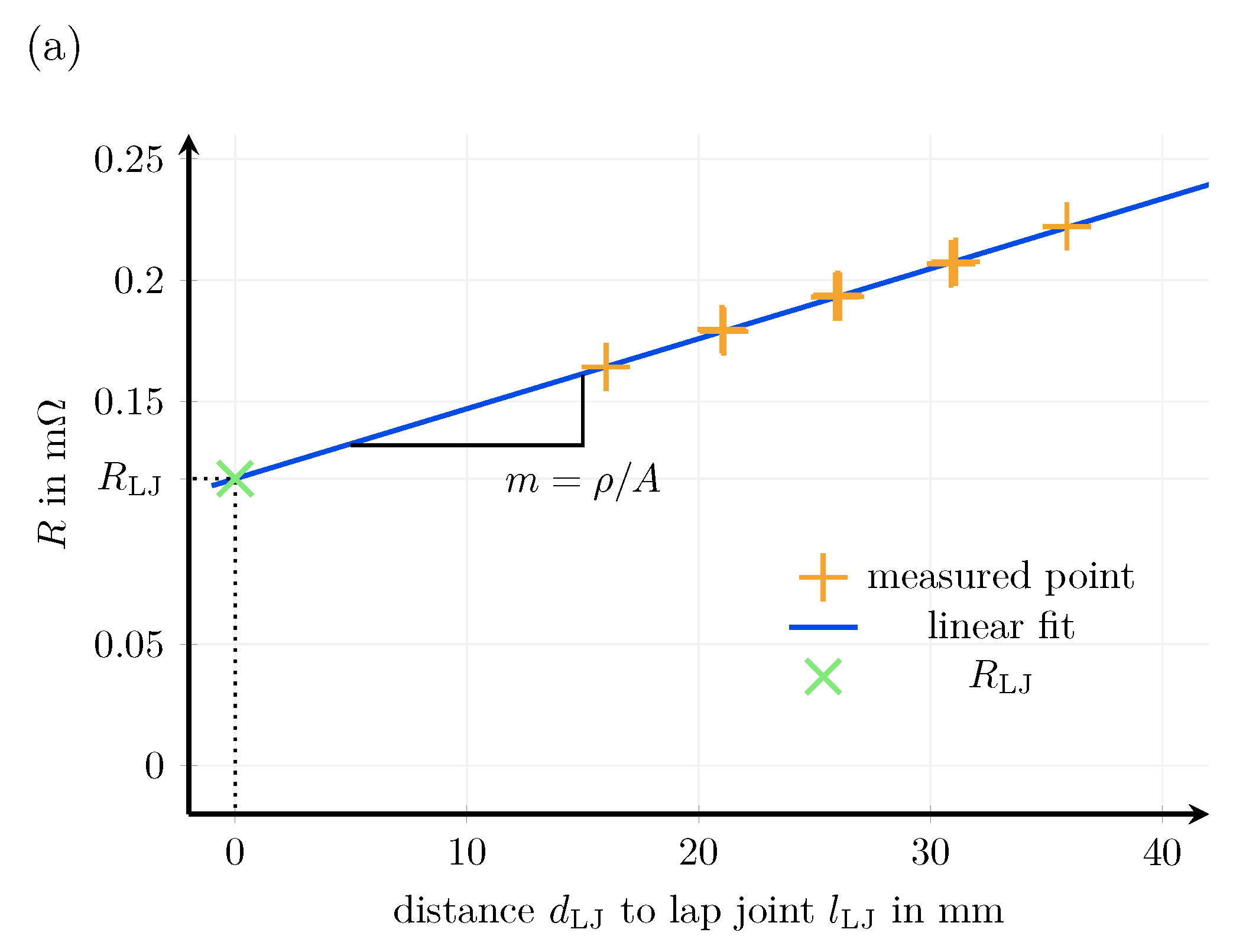
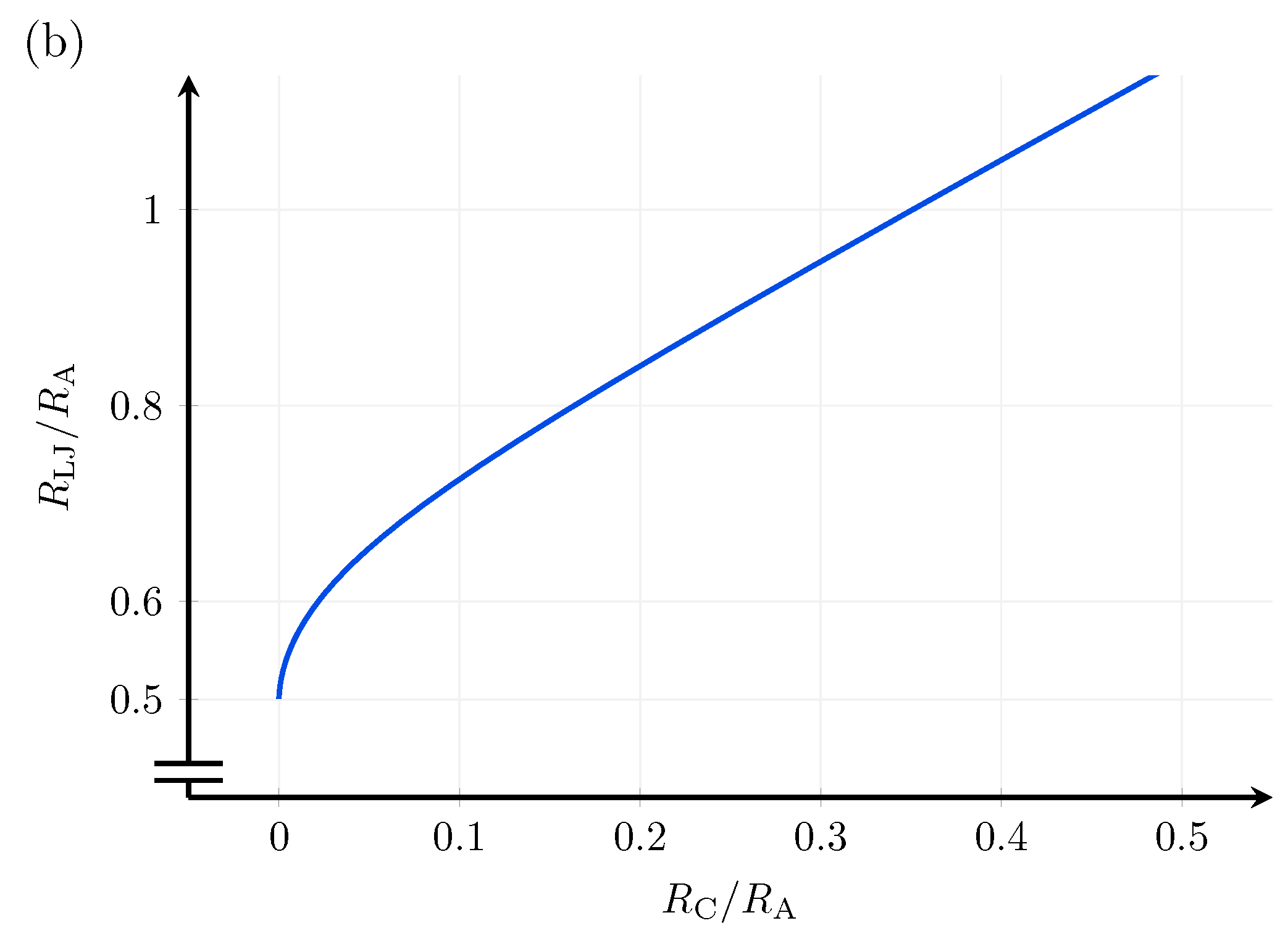
3.1.2. Method to Calculate the Electrical Connection Resistance within Planar Contacts

After having defined a measurement procedure and having identified the influences on the measurement, the calculation method within planar contacts for electrical connection resistance is discussed. For this purpose, the first step is to answer the questions as to how the contact resistance is obtained and how it can be determined. Similarly to soldered connections, a third conductive material is added between two specimens for adhesive connections. With the additional conductive partner, the resistance is split into the resistances of the specimens, ( R A and R B ); the contact resistance ( R C ), which is the sum of the surface resistance between the specimens and conductive adhesive; R S 1 and R S 2 ; and the resistance of the conductive adhesive layer ( R L ). The value of R C can be determined based on the values of R A , R B and R L , which are known parameters.
Additionally, as a planar contact is obtained when using an adhesive, the current distribution over this planar area needs to be investigated. To justify an area-based contact resistance, a parameter study in an FEM-simulation was performed. For all studies, a homogeneous surface resistance was used.
Figure 4 shows the normalized current through specimen A over the normalized lap joint ( l LJ ) in the y direction. Four different values for the contact resistance ( R C ), which depend on R A and R B , were chosen. Additionally, it is assumed that the current does not flow across the third partner. This phenomenon results when the layer thickness is small and the specific resistance of the third conductive partner is sufficiently high. As shown in Figure 4, three cases were investigated to demonstrate the influence of low, high, and two different medium contact resistances on the current distribution over the lap joint.
For this simulation analysis, the previously defined parameters were used ( σ brass A , B = 15.5 · 10 6 S/m and A A , B = 2   mm × 15   mm ).
High contact resistance: A high specific contact resistance ( R C A = 1 · 10 8 Ω m 2 ) results in a linear current distribution through the contact area, indicated by the orange line in Figure 4. The current through specimen A decreases linearly. The current flows homogeneously through the contact area, and a larger contact results in a lower contact resistance. In this case, the contact area determines the magnitude of the contact resistance.
Low contact resistance: A low specific contact resistance, e.g., R C A = 1 · 10 11 Ω m 2 , results in two separate current flows: one at the beginning and one at the end of the lap joint, as represented by the brown line in Figure 4. Although an electrical connection is present over the whole area between the specimen and the adhesive, only a minimal current flows through the middle of the specimen. This leads to the current remaining within the specimen and remaining constant. The current is divided according to the resistance of the specimens and forms an ideal parallel connection, resulting in non-linear behavior between the contact area and the resulting resistance. The distance between the contact area’s start and end primarily defines the contact resistance.
Medium contact resistance: Specific contact resistance in the range between the two cases discussed above ( R C = 1 · 10 9 Ω m 2 and R C A = 1 · 10 10 Ω m 2 ) results in a non-linear current distribution through the contact area, as represented by the pink and blue lines in Figure 4, respectively. Additionally, the current through the middle of the lap joint at l LJ = 7.5   mm in Figure 4 is divided according to the resistance ratio of both specimens ( R A and R B ).
In summary, no straightforward relation between contact resistance and contact area exists. However, the contact resistance does depend on the resistance ratio ( R C / R A ). The assumption of Brand et al. [4] to use a simplified version of the Equivalent Circuit Diagram (ECD) for area-based resistance is only valid if the contact resistance is lower than the resistance of the specimens. Additionally, Schmidt [36] analyzed the influence of the weld seam’s position on electrical properties. The connection showed the lowest resistance with two weld seams that were aligned as far apart as possible. This can be extended analogously to low contact resistance.
Generally, it cannot be stated that a larger contact area leads proportionally to a lower contact resistance. For the geometry investigated in this work, the primarily target is not to contact a large surface but to place the contact points as far apart as possible and to establish a parallel connection. The results of this study are relevant to all types of joining techniques and can be utilized to optimize and design the joining layout. For other geometries, such as cylindrical cells, the inner structure of the geometry has a significant influence. In this case, the contact points should be selected depending on the internal current flow. Lin et al. [37] defined this phenomenon at the end of the contact region as “current crowding” by investigating the wafer bonding process of microelectromechanical systems.
Nevertheless, the question of how to determine the contact resistance ( R C ) remains. For the analytical solution, the measured resistance over the lap joint ( R LJ ) and the resistance of the two specimens ( R A and R B ) are defined as known quantities, and the contact resistance is defined as the desired quantity. The branched electrical circuit model (ECM) relationship and the following simplified recursive formula (see Equation (3)) are derived in Appendix D.
R LJ k ( r a k , r b k , r a , r b , r c ) = s a + R LJ k 1 r ˜ a k 2 , r ˜ c k 1 , r a , r b , r c with r ˜ a k 2 = r a k 2 + s b and r ˜ c k 1 = s c = r a k ( r b + r c k ) r a k + r b + r c + r c k +   R LJ k 1 r ˜ a k 1 , r ˜ c k 1 , r a , r b , r c with r ˜ a k 1 = r a + r a k r c r a k + r b + r c + r c k and r ˜ c k 1 = r c ( r b + r c k ) r a k + r b + r c + r c k
Variables s a , s b , and s c represent resistance after a Δ -star transformation (see Appendix D). Equation (3) is only valid if it is assumed that no current flows across the third partner in the y direction. The resistors ( r c ) correspond to the equivalent circuit of a conductive adhesive joint, as illustrated in Figure A6.
Figure 5b depicts an example of the graphical determination of the contact resistance ( R C ) in the case of R A = R B based on Equation (3). With a contact resistance of R C = 0, an ideal parallel connection results and the R LJ / R A ratio is equal to 0.5 . Furthermore, linear behavior results at high contact resistance ( R C ). For a better understanding of the cases discussed above, Appendix C.1 discusses the resulting analytical contact resistance of a branched network. A similar result was published by Euler and Nonnenmacher [38].

3.1.3. Performing the Measurement

A fixture over an extruded aluminum rail was constructed to minimize possible position fluctuations. A picture is provided in Figure A1. Additionally, the distance between the power and sense pins for this investigation was set to a minimum of 10 mm to achieve an error below 0.05%. The distances between A m and B n = 1 4 were set to 5 mm, (c.f. Figure 2). Finally, all reasonable combinations of the sense pins ( A m and B n ) were measured via an MUX. Figure 5a exemplarily illustrates the measured resistances used within a linear interpolation to l LJ to determine R LJ . The distance ( d LJ ) is defined as the difference in the spacing between the sense pins ( A m and B n ) and the overlap length ( l LJ ). Assuming two identical specimens (A=B) are connected to each other, the specific resistance of the material can also be determined via the slope (m) and the specimen’s cross-sectional area (A) (see Equation (4) and Figure 5a).
ρ A , B = m A , B · A A , B
Subsequently, the recursive formula (Equation (3)) is solved based on the material resistance across the lap joint ( R A and R B ) and the resistance ( R LJ ), as shown in Figure 5b. The contact resistance ( R C ) can then be determined via the relationships of R LJ over R A and R C over R A .
Theoretical considerations can be utilized, regardless of the measuring device and joining technique. The subsequent analysis examines and compares electrically conductive adhesives with other well-established techniques. Moreover, the behavior of the ratio between contact resistance and contact area is demonstrated.
As specified by the manufacturer, the adhesive was mixed at a gravimetric ratio of 100:10 (resin (part A) to hardener (part B)), with an additional gravimetric 1% of spacer particles. Each sample was pressed with a weight of 60 g and cured for at least 24 h at room temperature. For each thickness ( h L ), a separate batch of the two-component adhesive was mixed. Thus, measurement data with the same adhesive thickness ( h L ) can be compared, and a scattering of the adhesive batches among each other can be assumed to be negligible. Before adhesive bonding, each specimen was cleaned with isopropanol to minimize surface inaccuracies between samples.
In order to determine the UTF of the samples joined with ECA, tensile tests were performed using the a Zwick Roell Z020universal testing machine (UTM) according to DIN EN 2243-1. Beyond the UTF of the lap joints, tensile tests can also provide additional information. In particular, an analysis of the fracture mechanisms provided insights into the joint’s limitations and the quality of the manufactured joint. Adhesive, cohesive, and substrate fracture mechanisms were expected from these tensile tests. While an adhesive fracture is caused by adhesion between the adhesive and substrate being the weakest point, a cohesive fracture results from broken bonds within the adhesive. In the case of a substrate fracture, the specimen material’s tensile strength is lower than that provided by the adhesive’s adhesion and cohesion. In this context, a substrate fracture provides the least information concerning the adhesive’s mechanical properties [39].

4. Results

In order to pursue the research objectives specified in Section 1, a variety of testing methods and materials were used to investigate dependencies in the contact area, the adhesive’s layer thickness, and specimen material concerning the R C and UTF. Table 1 shows the measured properties. The failure mechanism for UTF determination involved either adhesive (A) or cohesive (C) fracture. In addition to the expected value (μ and 90% confidence interval (CI) of the R C and UTF, the ratio of R LJ / R A is also provided in Table 1. The number of test samples for each step was five.
As expected, all measurements demonstrate a low R C and high UTF for an increased contact area. In addition, the results indicate a significant influence of the used specimen material on the contact resistance. The copper samples exhibit lower R C and UTF values. This can be attributed to different surface properties of the copper and brass samples, ( R S 1 and R S 2 [40]). The increasing adhesive layer thickness deteriorated the contact quality, leading to an increase in the R C and a decrease in the UTF. This was also discovered for the mechanical strength by Habenicht [40].
Among the brass samples, excluding the sample with the thickest adhesive layer (124 µ m ), a cohesive (C) fracture occurred. The brass samples with a 124 µ m adhesive layer thickness and all copper samples showed adhesive failure (A). This is also visible in the UTF measurement results in Table 1. The corresponding force–displacement curves are illustrated in Appendix B, Figure A2. Similar to the results of Habenicht [40], an increased lap joint length enhances the UTF, whereas with higher layer thickness, the UTF decreases. Figure 6b displays an example of a cohesive (C) fracture of silver-filled two-component epoxy-based adhesive with a contact area of 10 × 15 mm 2 and a layer thickness of 38 µ m .
Given that the influences of measurement were quantified and reduced in the preceding section, it is assumed that the sample scatter is substantial, despite the use of isopropanol to clean the surfaces. Furthermore, it can be affirmed that the variation was reduced for a larger area, which may be attributed to the bonding process employed in the laboratory. Nevertheless, it can be concluded that the contact resistance is characterized by low magnitudes of 10.53 µ Ω and 74.62 µ Ω when considering the expected values in an area of 15 × 15 mm 2 .
In general, an increased contact area results in lower contact resistance. For both investigated materials, increasing the lap joint length ( L LJ ) from 5 to 10 mm reduces the R C by about half its value. This correlation is invalid if the length is increased to 15 mm, which is three times the original length. In this case, the theoretical knowledge from Figure 5b and the R LJ / R A relation are considered. The linearity of R C ’s behavior depends on R LJ / R A when non-linear or linear behavior of the R C is present, assuming a contact-area-related resistance is only justified with a linear ratio, as described in Section 3.1.3. However, this does not hold true for copper and brass substrates. The R C is not in the linear domain. In this range to a first approximation, the contact resistance is no longer determined by the contact area but by the distance between the first and last contact conditions. An ideal parallel circuit can be assumed as a limiting value, and the R LJ / R A ratio converges toward 0.5 . This statement is valid as long as a relatively thin layer of the ECA is applied and the conductivity of the adhesive is higher than the conductivity of the specimen material. If the third conductive partner is thicker and has very high conductivity with respect to the metal to be joined, the ratio can be less than 0.5 . In that case, a current flows through the additional conductive partner in the y direction. The contact conditions keep the resistance low, as is the case when both materials are ideally connected.
In order to assess the layer thickness and the uniformity of the adhesive bonds, microscopic images were captured using a Keyence VR 3100 profilometer. Figure 6a indicates the layer thickness from the intended 124 µ m spacer. It is apparent, however, that the layer thickness is not entirely uniform across the adhesive layer. In this case, it has a thickness of approximately 130 µ m . Additionally, Figure 6a illustrates that the two specimens were bonded parallel to each other.

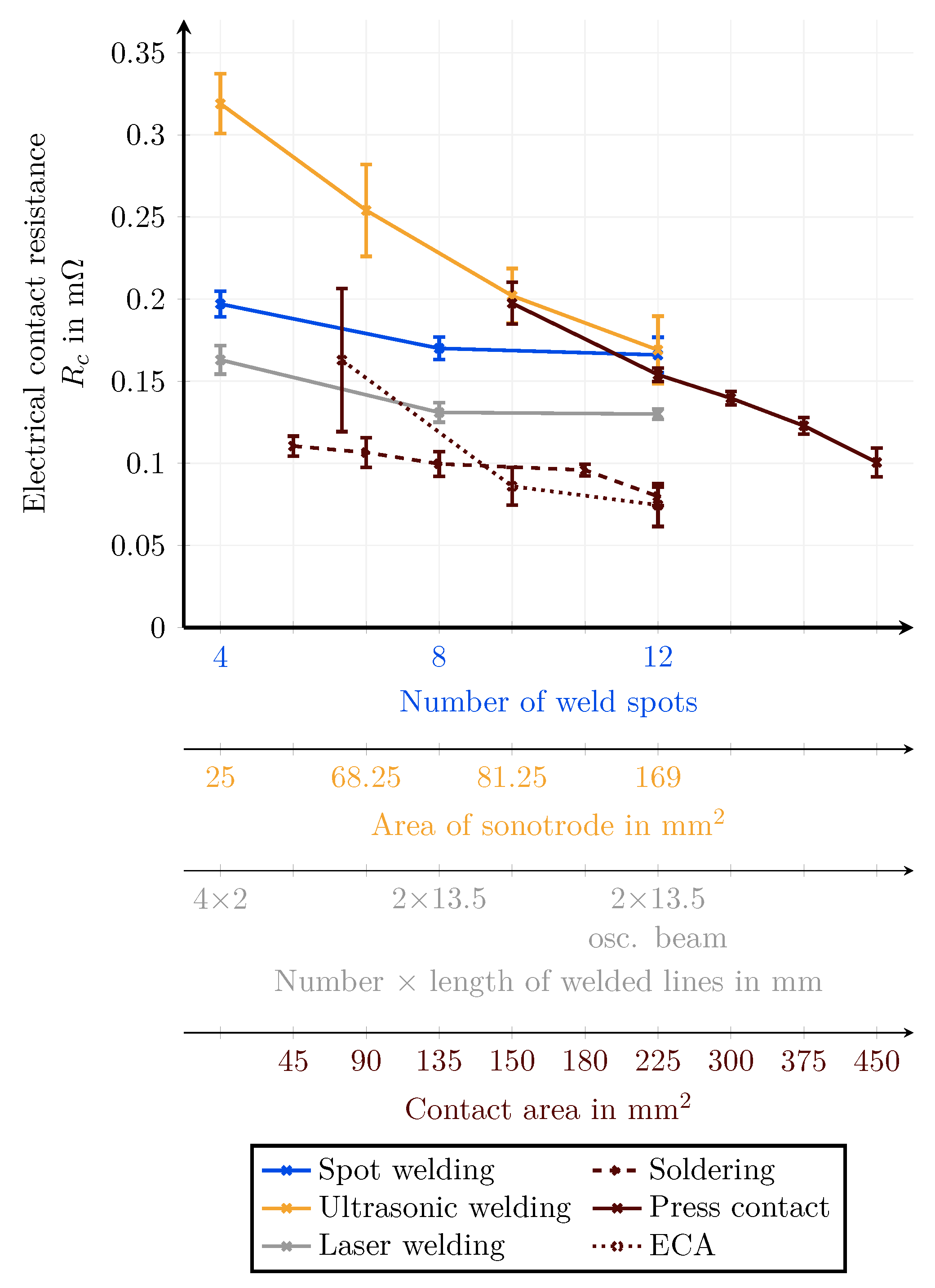
4.1. Comparison of Joining Techniques in Terms of Electrical Connection Resistance and Ultimate Tensile Force

In this section, the investigated ECA is compared to other electrical joining techniques regarding R C and UTF, which results from the brass substrate. Figure 7 shows the R C of ECA in comparison to soldering, spot welding, ultrasonic welding, laser beam welding, and press contact, which were investigated by Brand et al. [4]. The abscissa from Brand et al. [4] was applied to depict the ECA for soldering and press contact. Caution regarding the ECA abscissa is required, as the abscissa exhibits a linear progression up to 225 in 45 increasing intervals. However, starting from 225, the interval between the values increases to 75. The contact areas of the ECA are 5 × 15 mm 2 , 10 × 15 mm 2 , or 15 × 15 mm 2 . According to the investigated brass samples, ECA lies in the range between welding and soldering. With a contact resistance of 74.62 µ Ω , it exhibits the lowest resistance compared to the connection techniques investigated by Brand et al. [4]. Contrary to Brand et al. [2,3,4], the brass samples in this study were measured with a thickness of 2 mm to minimize the measurement errors (see Section 3.1.1). Additionally, Brand et al. [4] conducted experiments with the BT3562 measurement unit of the Hioki E.E. Corp. The alternating measurement current was set to 100 mA at a frequency of 1000 Hz.
In addition, the UTF of well-established joining techniques was compared to the respective ECA. Figure 8 provides a quantitative overview of ECA, soldering, spot welding, ultrasonic welding, laser beam welding, and press contact. Again, Brand et al. [4] provided the data on well-established joining techniques. The soldered specimens fractured due to material fatigue and did not break at the joint. As previously mentioned, specimens ten times thicker were used in this work and reached the highest mechanical tensile force of 2519 N at a contact area of 15 × 15 mm 2 with ECA.

4.2. Discussion

The present study illustrates that electrically conductive adhesives (ECA) can achieve similar magnitudes of electrical conductivity and mechanical strength as those attained by well-established electrical contacting techniques. While several ECAs were assessed, only PT EC 244 exhibited results comparable to those of well-established joining techniques for battery applications. Consequently, only one adhesive is presented here. Furthermore, while the copper samples exhibited a lower electrical contact resistance than brass, the brass samples had higher mechanical strength. These two characteristics are assumed to depend on the condition between the specimens’ surfaces and the adhesive. The characteristics can be transferred with regard to the condition of the specimens. In addition, ECA demonstrates several advantages over well-established electrical joining techniques. Depending on the adhesive, the gluing process does not require heat input for soldering or welding. It is, therefore, suitable for temperature-sensitive components, such as lithium-ion batteries [4]. Due to the lack of heat input, no residual stresses remain in the connection after the joining process.
However, disadvantages are that the adhesive is cost-intensive, and scattering of the joint’s properties can also occur in small quantities. Furthermore, the adhesive requires a resting period for curing, which can be shortened by heat input. The adhesive used in this experiment was cured at room temperature for 24 h. In particular, a pot time of 15 min could make this method problematic in many of the assembly processes for manufacturers. However, if a high temperature does not harm the application, PC 3001 from Heraeus can also be considered as a possible adhesive. An internal preliminary study showed similar electrical resistance and mechanical strength results compared to the investigated EC 244 from Polytec. However, PC 3001 was unsuitable for battery applications because it required a curing temperature of over 120 C .
The electrical contact resistance is not just determined by the process and material composition but also by the geometrical and electrical parameters of the elements being connected and the arrangement of the contact points. As demonstrated in this paper, it is not necessarily a larger contact area that is important but the distance between the two outer contact lines. This should be taken into account when evaluating the electrical contact resistance.

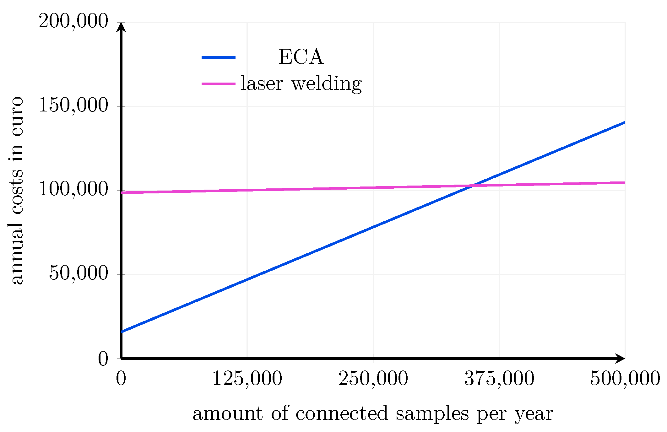
4.3. Economic Evaluation

The resulting electrical and mechanical joint properties are visualized in Figure 7 and Figure 8 in comparison to other joining techniques. Since laser beam welding is commonly used for mass production in battery contacting, it was used as a reference for the economic assessment of ECA. To manufacture planar contacts using ECA, a plant producing adhesives worth EUR 50,000 was defined. For laser-based joining, a setup that includes a laser cell, chiller, laser beam source, and scanner optics for EUR 455,000 was assumed. The costs for both systems were requested from the respective manufacturers. For both joining processes, the machine costs per hour were calculated according to VDI guideline 3258 A, where the machine costs per hour, the labor costs, and the cycle times are considered. Appendix E, Table A1 and Table A2 provide a detailed overview of the costs. For ECA, there are two different curing approaches. On the one hand, a temperature of 80 C can be applied for 15 min, whereas, on the other hand, curing can take place at room temperature for 24 h. Since the former may harm the battery cell, the latter was chosen. Regarding the calculation, additional space for curing was considered and approximated by a square that fits a cylindrical cell (18 mm by 18 mm for a 18,650 cell, for example). Figure 9 shows a comparison of the two joining methods.
Furthermore, it was considered that the costs of a connection for ECA depend on the joined area. A selection of joining areas for frequently used cell geometries and the accompanying costs for ECA and the spacers are provided in Figure 10. A detailed overview of the calculation is listed in Appendix E, Table A3. A large cost factor is the material costs of the adhesive. In this publication, a price of 5 kg was used for the calculation. It is assumed that this cost will decrease with mass production
Figure 9 clearly demonstrates that the costs for ECA in series production are significantly higher than those for laser beam welding. Nevertheless, ECAs is competitive with established joining processes concerning physical properties. This is why ECA may be a suitable alternative to manufacturing planar contacts for prototyping and development projects.

5. Conclusions

This study introduces a method to analyze the electrical resistance of planar contacts based on their area. The method allows for identification of whether the contact resistance of the joint demonstrates linear or non-linear behavior. It is suitable for all electrical connection techniques and can help to optimize contact geometries. Based on this, electrical adhesive connections were analyzed based on their electrical and mechanical properties and through an economic assessment and compared with well-established contacting techniques.
Regarding the first research question, it was demonstrated that current injection considerably influences voltage measurement and accuracy. The former is particularly important when determining electrical parameters and when high accuracy is required. Through mathematical consideration, the error between the linear and the theoretical values was determined using Poisson’s equation. The error decays to zero depending on the sample’s dimensions. The distance between the power and the sense pins should be set to a minimum of half of the longest side length of the specimen’s cross-sectional area (A). Concerning the second research question, the current is divided according to the resistance of the specimen and the contact. For this purpose, a correlation was mathematically determined to verify whether the measurement occurs in a non-linear or linear relationship between contact area and contact resistance. According to the derived method, the current is divided by the current divider in the non-linear range. In this case, the contact resistance is primarily affected by the length of the contact area but not by the cross-sectional area. Finally, based on the third research question, epoxy-based silver-filled adhesive joints were compared to other well-established contacting techniques [2,3,4], such as welding, press connections, and soldering, and were found to have a low contact resistance and a high mechanical strength. For brass samples with a contact area of 15 × 15 mm 2 and a thickness of 38 µm, an electrical contact resistance of 74.62 µ Ω and an ultimate tensile force of 2519 N were observed.
Moreover, an economic assessment was conducted to compare the investigated ECA and the equipment for laser beam welding. The results indicate that for series production, costs for ECA are significantly higher than for laser beam welding. It is assumed that the cost of ECA will decrease with mass production. However, ECAs is competitive with established joining processes concerning electrical and mechanical properties.
Further studies should be conducted in an attempt to minimize sample scatter in the form of pretreated materials. Other environmental influences, such as humidity and temperature, on the contact resistance ( R C ) or the current-carrying capacity should be investigated. Another interesting research topic is the aging behavior of the joints under the influence of the abovementioned environmental aspects.

Author Contributions

Conceptualization, P.J.; methodology, P.J. and M.R.G.; software, P.J.; validation, P.J. and A.V.H.; formal analysis, P.J., M.K.K. and M.R.G.; investigation, P.J., M.K.K., A.G., A.V.H. and E.H.; resources, M.F.Z. and A.J.; data curation, P.J.; writing—original draft preparation, P.J.; writing—review and editing, P.J., M.K.K., M.R.G., A.G., M.F.Z. and A.J.; visualization, P.J.; supervision, A.J.; project administration, A.J.; funding acquisition, M.F.Z. and A.J. All authors have read and agreed to the published version of the manuscript.

Funding

This research was funded by the German Federal Ministry of Education and Research (BMBF) and the German Federal Ministry of Economic Affairs and Climate Action (BMWK) via the OSLiB research project (grant number 03X90330 A) and ultraBatt (grant number 01MV21015D). The projects were overseen by Project Management Juelich (PtJ) and DLR Projektträger, respectively.

Data Availability Statement

Data are available upon request.

Acknowledgments

The authors thank Korbinian Schmidt, Chair of Electrical Energy Technology at the Technical University of Munich, for supporting the investigations with practical workmanship.

Conflicts of Interest

The authors declare no conflict of interest. The funders had no role in the design of the study; in the collection, analyses, or interpretation of data; in the writing of the manuscript; or in the decision to publish the results.

Abbreviations

The following abbreviations are used in this manuscript:
Aadhesive
ACAanisotropically conductive adhesive
CIconfidence interval
Ccohesive
ECDEquivalent Circuit Diagram
ECMelectrical circuit model
R C contact resistance
ECAelectrically conductive adhesives
EVelectric vehicle
μexpected value
FEMfinite element method
ICAisotropically conductive adhesive
UTFultimate tensile force
MUXmultiplexer
NCAnon-conductive adhesive
UTFultimate tensile force
UTMuniversal testing machine
TCAthermally conductive adhesives
VDAGerman Association of the Automotive Industry

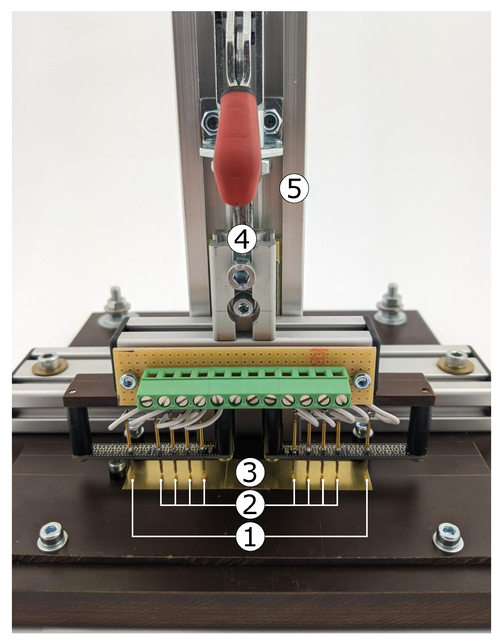
Appendix A. Test Bench

Figure A1. Custom-made test bench including gold-plated spring contact pins with a continuous plunger by Feinmetall GmbH. It contains two power pins ① to apply the measurement current and eight sense pins ② to measure the potential distribution over the sample under test ③. The geometric dimensions of the contact pins can be taken from Figure 2. The fixture ⑤ over the extruded aluminum rail ④ was used in order to minimize fluctuations in position.
Batteries 09 00443 g0a1

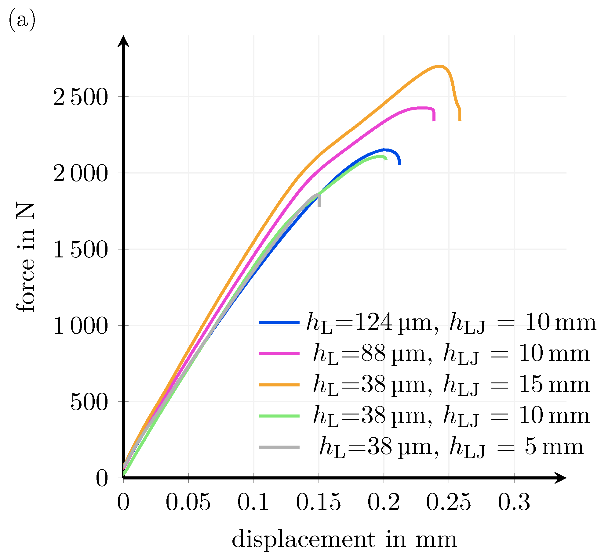
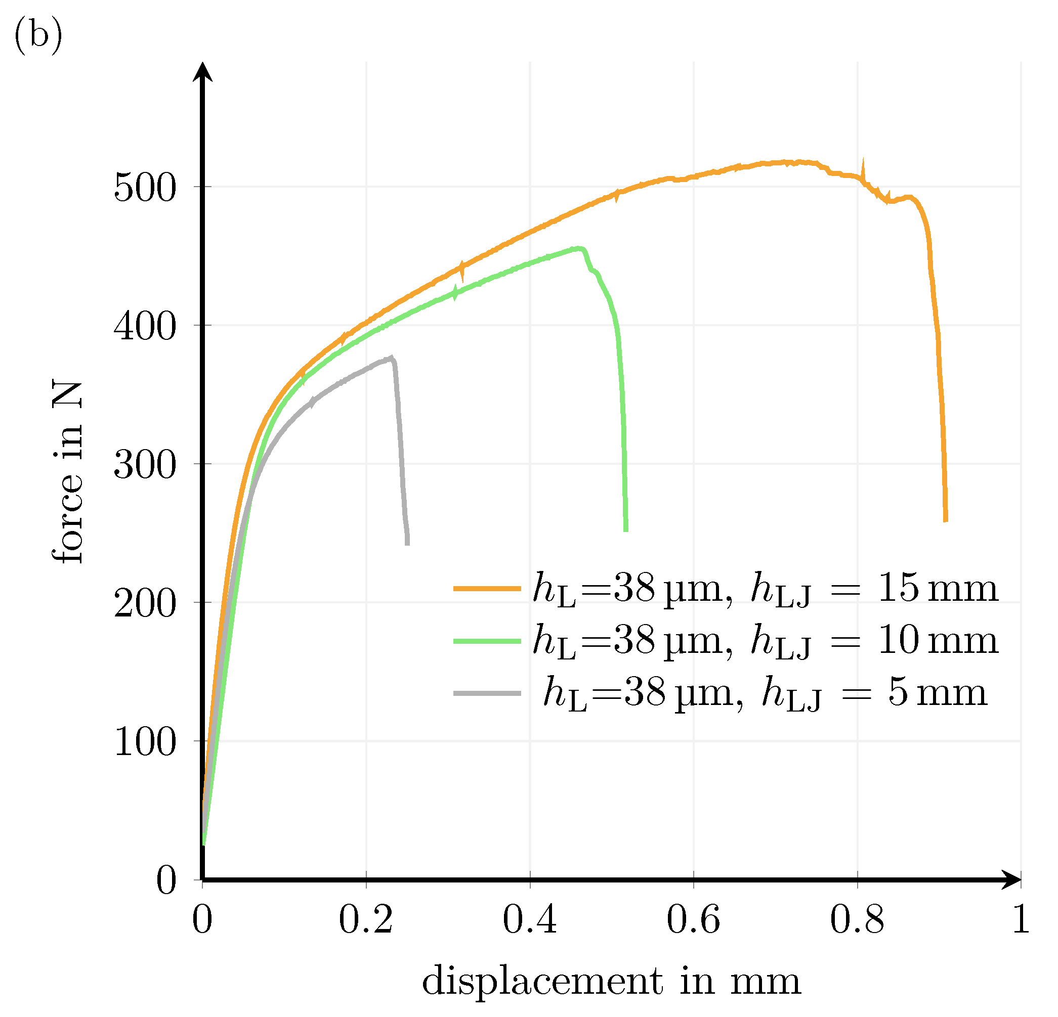
Appendix B. Force–Displacement Curve

Figure A2. Force–displacement curve of brass (a) and copper (b) samples for different adhesives layer thicknesses and lap joint lengths.
Batteries 09 00443 g0a2aBatteries 09 00443 g0a2b

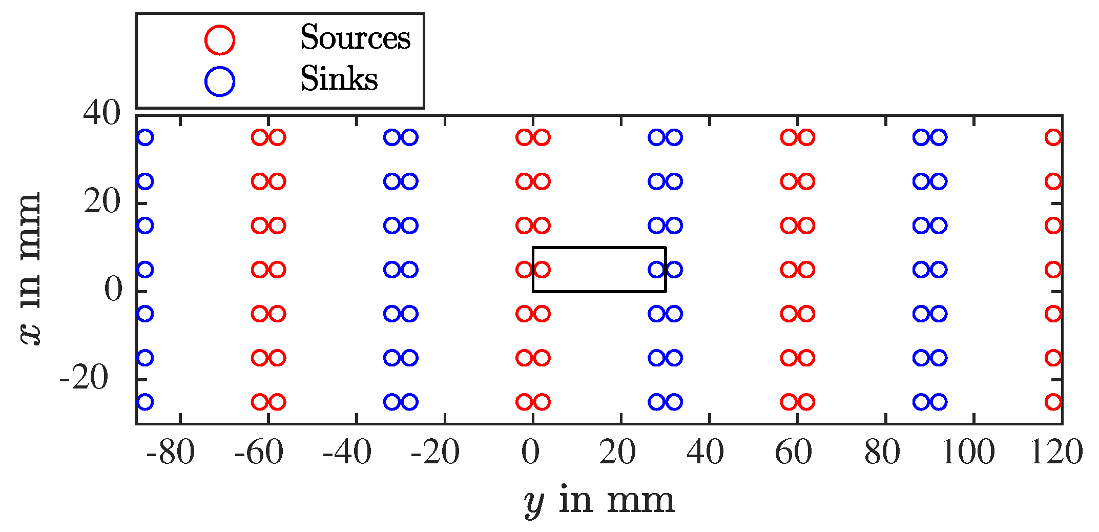
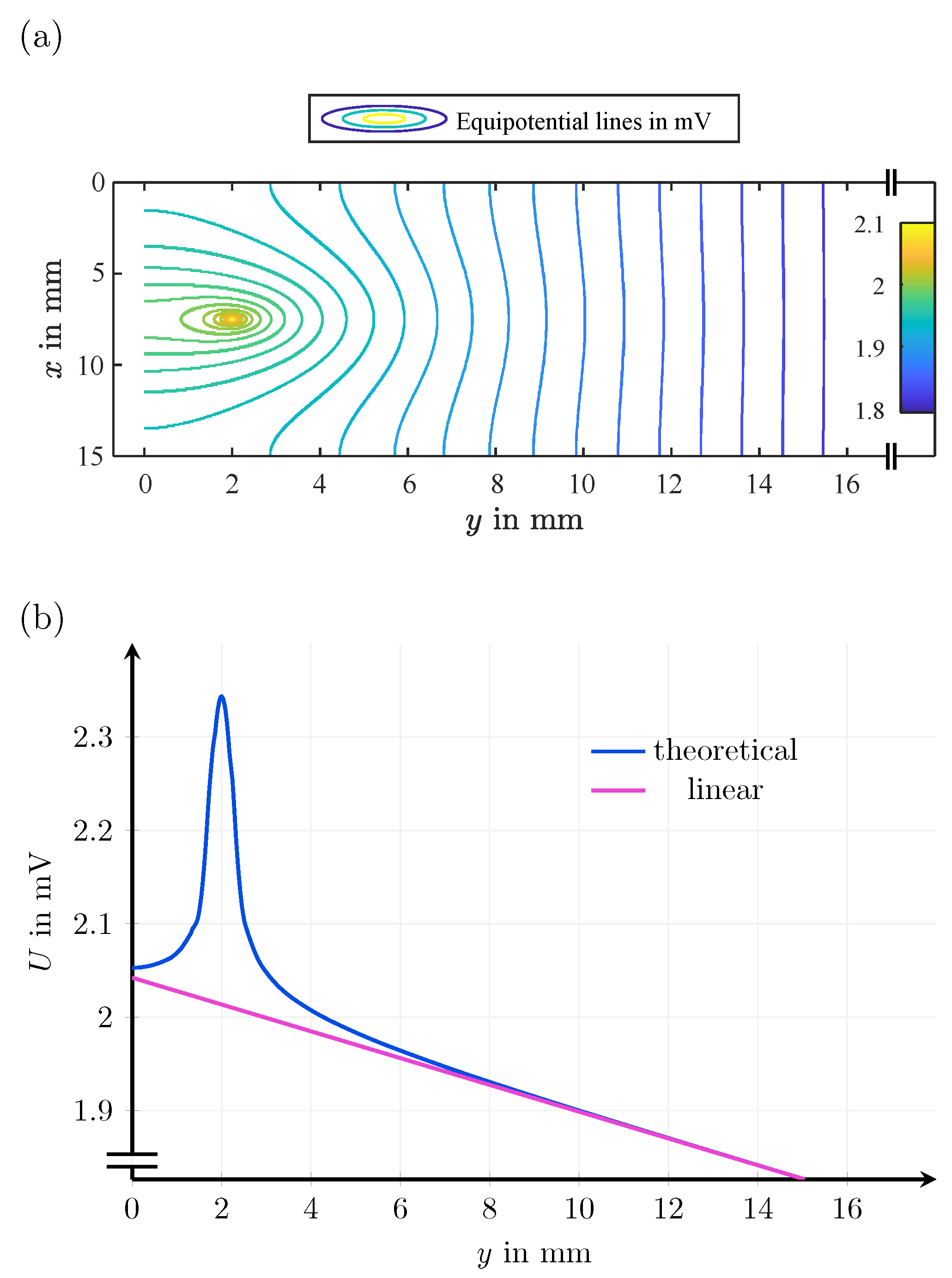
Appendix C. Theoretical Consideration of the Influence of Current Injection on the Voltage Measurement

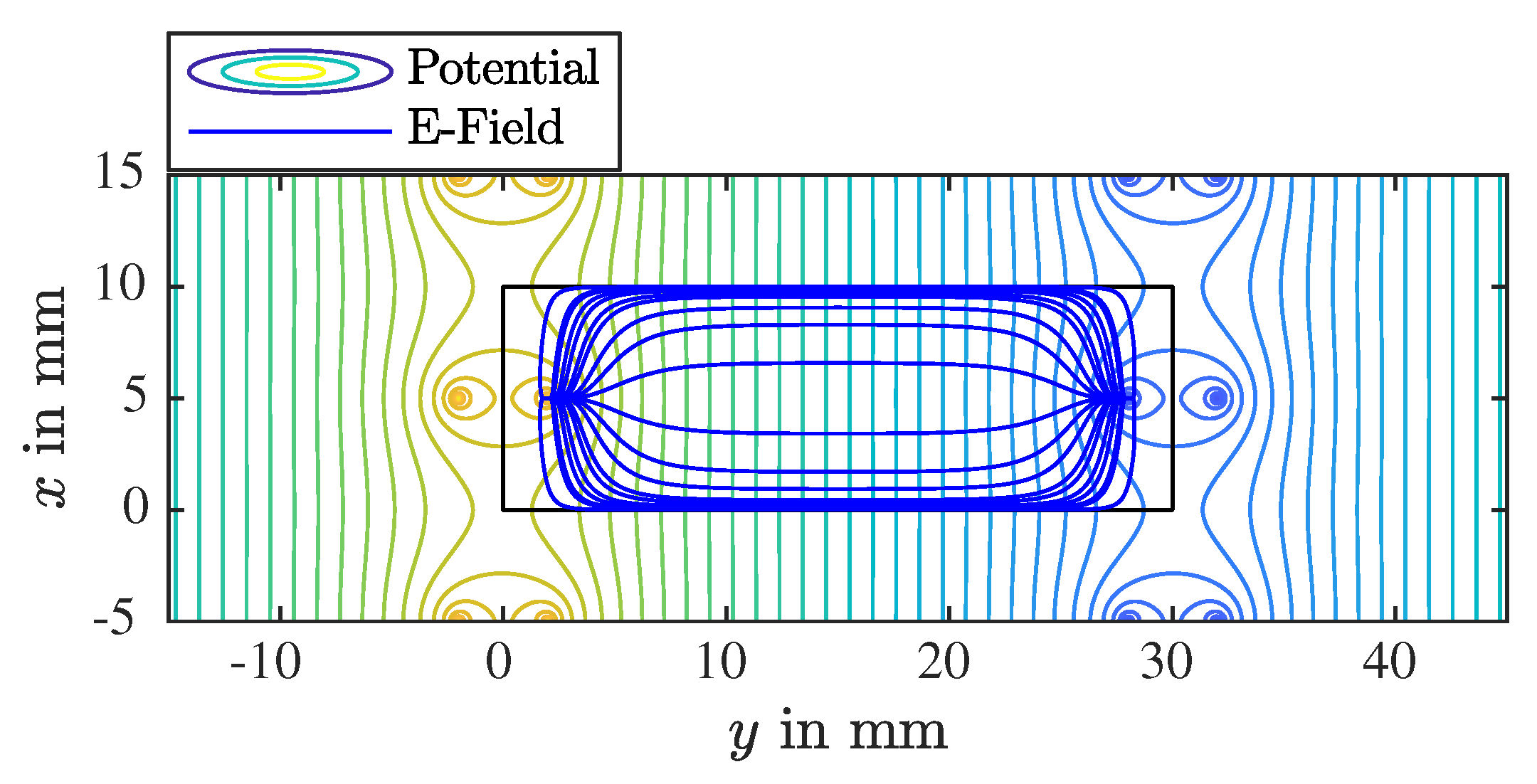
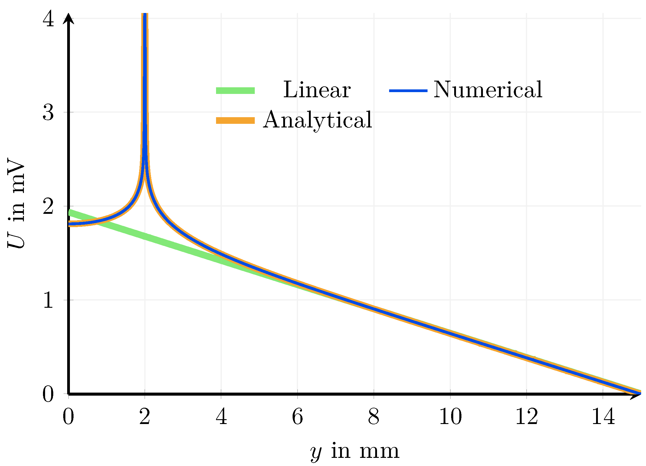
Appendix C.1. Formulation of the Problem

On an infinitesimally thick conductive plate with a width of w and a length of l at the position x 1 = ( x 1 , y 1 ) , a current (I) is induced into the plate. At another position ( x 2 = ( x 2 , y 2 ) ), a current of exactly the same strength flows out of the plane. In less abstract terms, this problem involves a metal plate with two needles pressed onto it, which function as contacts to an external ideal current source. Now, the task is to determine the potential field and the current density distribution inside the plate.

Appendix C.2. Governing Equations and the Infinite Plate Problem

Before considering a finite plate, the solution for an infinite plate is presented. Since the induced and extracted currents are constant, the problem can be assumed to be static, i.e., the electrical and magnetic fields ( E and B , respectively) are independent of time ( E ˙ = B ˙ = 0 ). In this case, the Maxwell equations describing the electric field (E) can be summarized by Poisson’s equation
Δ Φ ( x ) = ρ ( x ) ϵ ,
where Φ is the electric potential, ρ ( x ) is the charge distribution, and ϵ is the permittivity inside the plate. The electric potential can be calculated once the charge density is known using this equation. Now, the charge density in this infinite plate problem is described.
It is generally accepted that a current flow does not result in a charge buildup inside a conductor. The conductor stays neutral. However, if an attempt is made to induce a fixed current through an infinitely small cross section into a plate, the charge density ( j ( x ) ) is infinitely large. Under this condition, the charge neutrality is no longer valid. Therefore, only at positions ( x 1 , y 1 ) and ( x 2 , y 2 ) , where the current is being induced and respectively extracted, does the charge density not vanish. Instead, at these two positions, the charge density is expressed by two parameters: Q 1 and Q 2 . By using two Dirac deltas, the charge density can be mathematically expressed as
ρ ( x ) = Q 1 δ ( x x 1 ) + Q 2 δ ( x x 2 ) .
In order to find the as-yet-unknown parameters ( Q 1 and Q 2 ), Ohm’s law is applied:
j = σ E
where σ is the conductance of the plate. The integral of the current density around the source needs to be equal to the total current (I) that is being induced into the plate.
I = A d A j = A d A σ E = = A d V σ E = A d V σ ρ ( x 1 ) ϵ = Q 1 σ ϵ
Gauss’s theorem was used to transform the surface integral to a volume integral. Since this is a 2D problem, the surface is a line, and the volume is an area in this case. The prefactor of the Dirac delta function can be obtained by applying a volume integral enclosing the root of the Dirac delta function, which is position ( x 1 , y 1 ) .
If the charge density of a single source, i.e., ρ ( x ) = ϵ I σ δ ( x x 1 ) , is plugged into (A1), the potential of a source on a plate can be computed:
Φ 1 ( x ) = I 2 π σ ln ( x x 1 ) 2
The potential of a sink, i.e., the point where the current (I) is being extracted, can be computed similarly, with the only difference being a minus sign in the constraint of (A1).
Φ 2 ( x ) = I 2 π σ ln ( x x 2 ) 2
Since the Poisson equation is linear, the total potential of a sink/source system on an infinite plate can be simply determined by the superposition of Φ 1 and Φ 2 .

Appendix C.3. The Finite Plate Problem

In order to solve the finite plate problem, the linearity of Poisson’s equation is used again. Furthermore, because it is a solution for a certain charge distribution ( ρ ( x ) ) and a set of boundary conditions is unique, the boundary conditions are determined by the requirement that no current crosses through the boundaries of the plate, i.e.,
j · n = 0 ,
where n represents the normal vectors at the plate boundaries. As long as the boundary conditions are satisfied, charges can be added outside the finite plate without affecting the solution inside the plate. This is true because of the uniqueness of the solution of the Poisson equation. It is also possible to place charges outside the plate in a manner that still fulfills the boundary conditions, as described in more detail by Griffiths [41].
If the plate with the sink and source were only constrained in one direction, such as x > 0 , it would be sufficient to mirror the positions of the sink and source on the y axis. However, after introducing other boundary conditions, the source and sinks must also be mirrored on these new boundaries. This creates additional virtual sources and sinks that must be mirrored at the original boundary as well, leading to an infinite series of virtual sources and sinks, as shown in Figure A3.
According to [42], the coordinates of all sources or sinks that needed to express the finite plate problem for a source or sink at position ( x i , y i ) are given by
( x i + 2 m l , y i + 2 n h ) , ( 2 l ( m + 1 ) x i , 2 h n + y i ) , ( 2 l ( m + 1 ) x i , 2 h ( n + 1 ) y i ) , ( 2 l m + x i , 2 h ( n + 1 ) y i )
where m , n Z . The variable m is needed to describe all mirror sources that are necessary to fulfill the boundary conditions of the current density in the -direction, whereas the index n creates image sources to satisfy the constraints on the y component of j .
Figure A3. Mirror sources and sinks for an arbitrary position of the original source and sink.
Batteries 09 00443 g0a3
The full potential of the source and sink problem is obtained by adding up the potentials related to sources and sinks at these coordinates.
Φ Source / Sink ( x ) = I 2 π σ m = n = { ln x i + 2 m l y i + 2 n h x + ln 2 l ( m + 1 ) x i y i + 2 h n x + ln 2 l ( m + 1 ) x i 2 h ( n + 1 ) y i x + ln x i + 2 l m 2 h ( n + 1 ) y i x }
Φ tot ( x ) = Φ Source ( x ) + Φ Sink ( x )
The resulting potential field can be found in Figure A4. Figure A5 compares this analytical result with a numerical simulation. These numerical and analytical calculations align the most if, in the simulation, the radius of the current source, as well as the plate thickness, are set to be very small. Additionally, the mesh of the simulation was set to be extremely fine.
Figure A4. Potential distribution of the finite plate problem with a current of I = 1 and σ = 156.64   Ω 1 (effective 2D conductivity for a brass plate with a thickness of d = 0.01 mm ).
Batteries 09 00443 g0a4
Figure A5. Potential across the y axis; a numerical and analytical voltage curve compared to the ideally expected linear slope of Ohm’s law.
Batteries 09 00443 g0a5

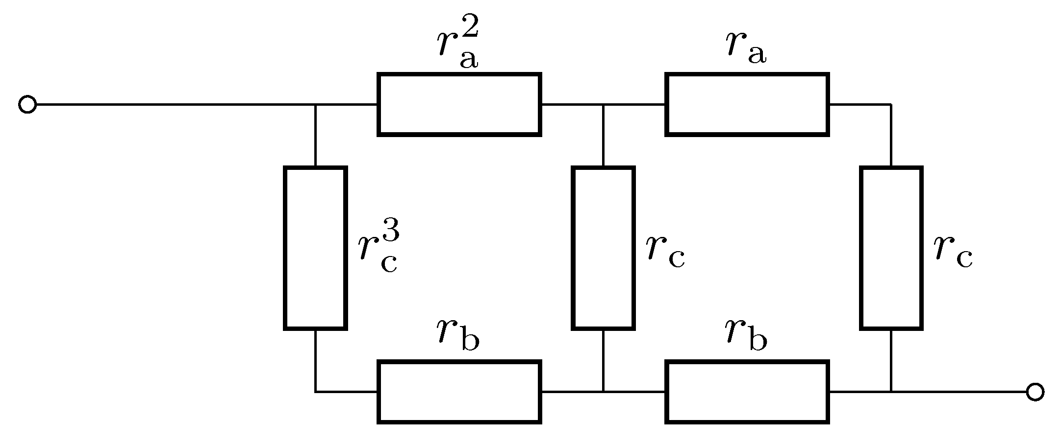
Appendix D. Resistance of An Adhesive Joining

Appendix D.1. Derivation of the Recursive Formula

Using the equivalent circuit depicted in Figure A6, the resistance of an adhesive joint can be calculated. In order to compute its total resistance for an arbitrary kP circuit (where k stands for the number of vertical resistors ( r c )), Δ -star transformations can be used to transform a kP into a ( k 1 ) P circuit.
Figure A7 shows the circuit after a Δ -star transformation applied to the leftmost loop, where
s a = r a k 1 ( r c k + r b k 1 ) r c k + r c k 1 + r b k 1 + r a k 1
s b = r a k 1 r c k 1 r c k + r c k 1 + r b k 1 + r a k 1
s c = r c k 1 ( r c k + r b k 1 ) r c k + r c k 1 + r b k 1 + r a k 1 .
This results in a ( k 1 ) P circuit in series with the resistor ( s a ), where the original resistor values of r a k 1 and r c k were changed to r a k 1 + s b and s c , respectively. All other resistor values remain unchanged. Therefore, their indices (k) can be omitted.
Figure A6. Equivalent circuit of a conducting adhesive joint.
Batteries 09 00443 g0a6
Figure A7. Equivalent circuit after a Δ -star transformation.
Batteries 09 00443 g0a7
Now, a recursive formula for the total lap joint resistance ( R LJ k ) of a kP circuit can be found:
R LJ k ( r a k , r b k , r a , r b , r c ) = s a + R LJ k 1 r ˜ a k 2 , r ˜ c k 1 , r a , r b , r c with r ˜ a k 2 = r a k 2 + s b and r ˜ c k 1 = s c = r a k ( r b + r c k ) r a k + r b + r c + r c k +   R LJ k 1 r ˜ a k 1 , r ˜ c k 1 , r a , r b , r c with r ˜ a k 1 = r a + r a k r c r a k + r b + r c + r c k and r ˜ c k 1 = r c ( r b + r c k ) r a k + r b + r c + r c k
Recursive reduction can be used until k = 3 is reached. Now, the 3P circuit shown in Figure A8 can be solved directly by a Δ -star transformation. The transformed circuit is depicted in Figure A9.
Figure A8. Base case for k = 3 .
Batteries 09 00443 g0a8
Figure A9. Base case for k = 3 after a Δ -star transformation.
Batteries 09 00443 g0a9
The resistor values ( S i ) are expressed as
S a = r a 2 ( r c 3 + r b ) r c 3 + r c + r b + r a 2
S b = r a 2 r c r c 3 + r c + r b + r a 2
S c = r c ( r c 3 + r b ) r c 3 + r c + r b + r a 2
and the total resistance of the 3P case is:
R LJ 3 ( r a 3 , r c 3 , r a , r b , r c ) = = S a + 1 1 S c + r b + 1 S b + r a + r c = r a 2 ( r c 3 + r b ) r c 3 + r c + r b + r a 2 + + 1 1 r c ( r c 3 + r b ) r c 3 + r c + r b + r a 2 + r b + 1 r a 2 r c r c 3 + r c + r b + r a 2 + r a + r c

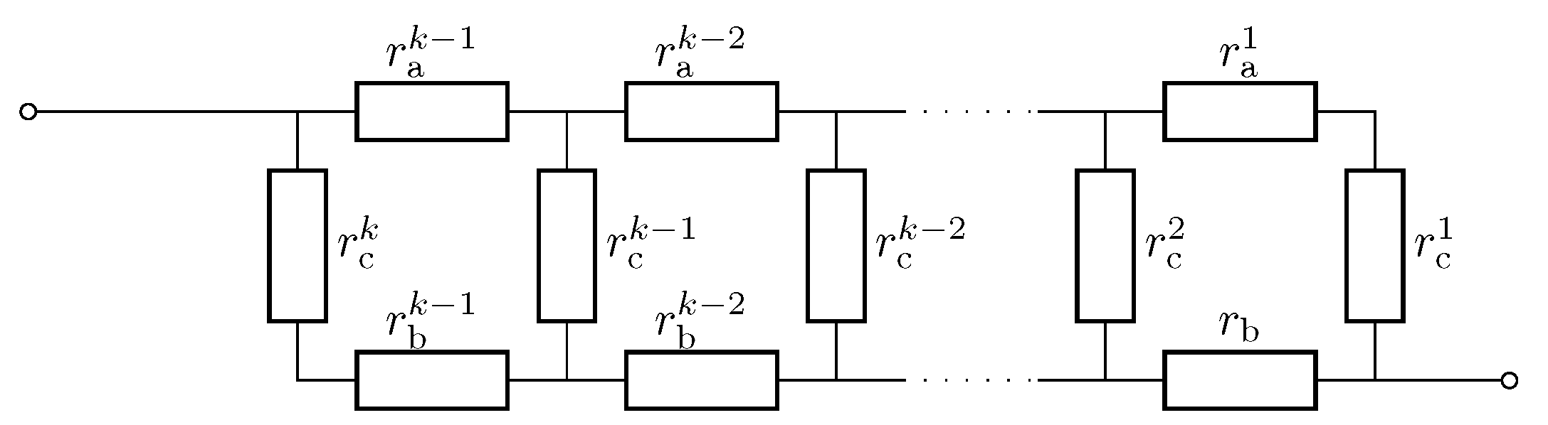
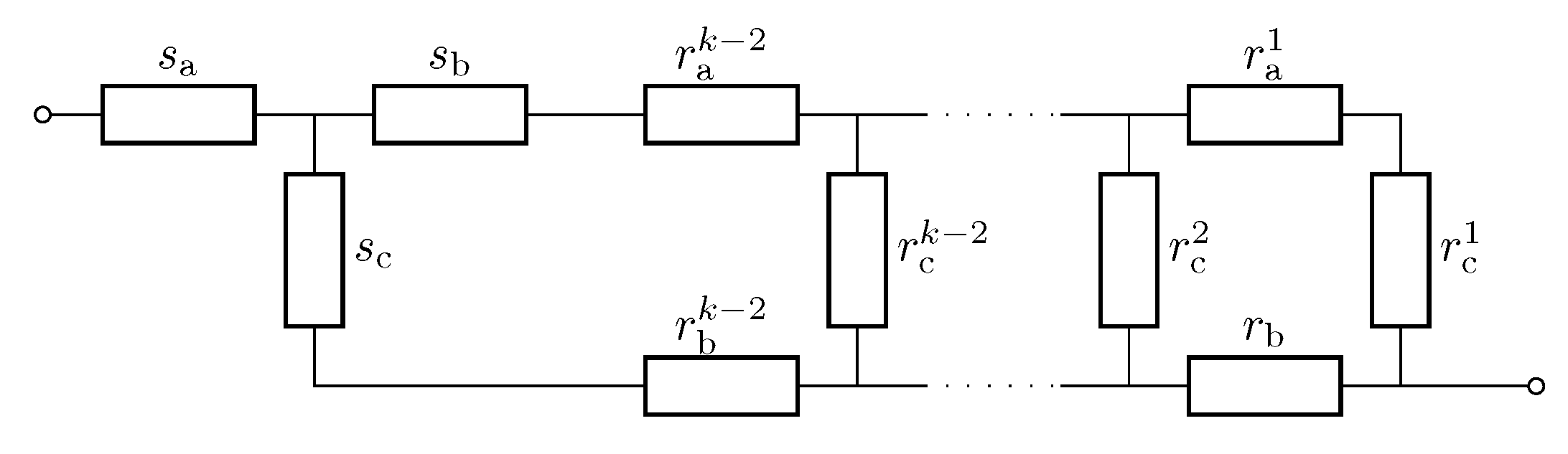
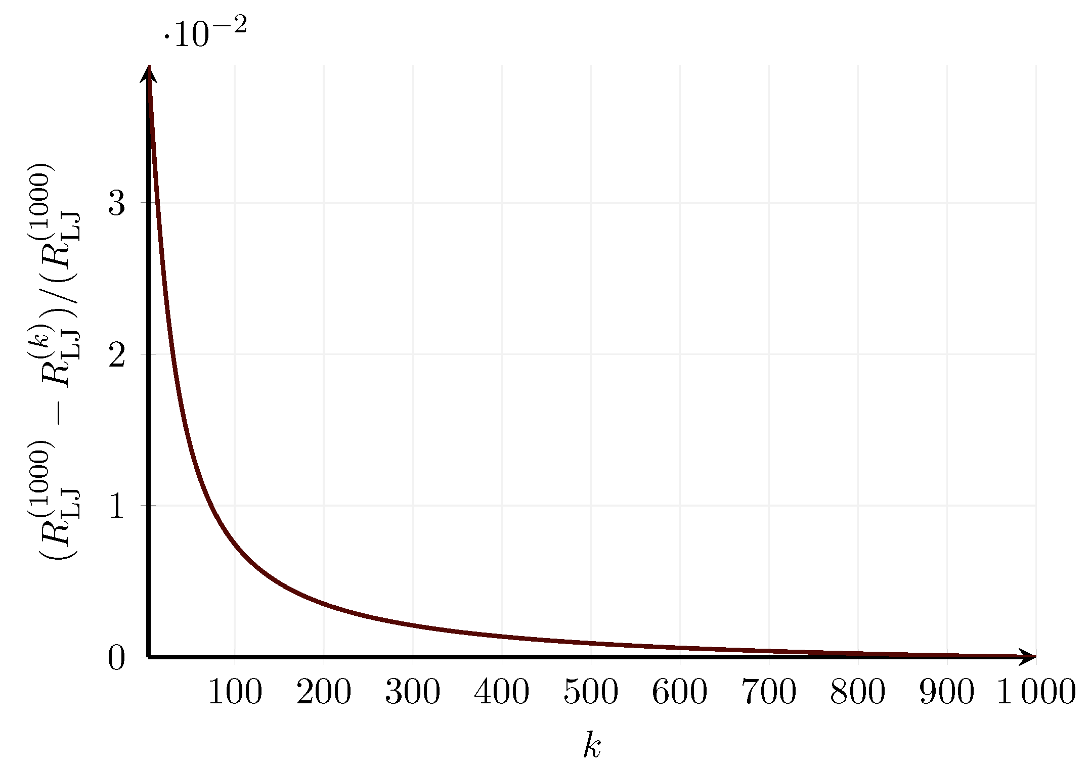
Appendix D.2. Convergence

In the equivalent circuit in Figure A6, r a , r B , and r c are differential resistors that must be connected to a finite macroscopic resistor to ensure convergence. As k increases, these macroscopic resistors are decomposed into an increasing number of differential resistors. Quantitative dependencies can be found for the two limiting cases ( r c and r a , r b 0 ). Then:
r A = R A k 1
r b = R B k 1
r c = k R C
After substituting these definitions into the recursive formula, R LJ k ( R A , R B , R C ) can be calculated for k = 3 , 4 , 5 . The following expressions can be found for the symmetrical case where R A = R B :
R LJ 3 = ( R A ) 2 + 12 R A R C + 18 ( R C ) 2 2 R A + 18 R C R LJ 4 = ( R A ) 2 + 16 R A R C + 24 ( R C ) 2 2 R A + 24 R C R LJ 5 = ( R A ) 3 + 55 ( R A ) 2 R C + 700 R A ( R C ) 2 + 1000 ( R C ) 3 2 ( R A ) 2 + 50 R A R C + 500 ( R C ) 2
Figure 5b shows the dependence of the total resistance on the input parameters ( R A , R B , and R C ) for the simplified symmetrical case with R A = R B . In Figure A10, the relative difference of a kP circuit compared to a 1000 P circuit is plotted.
Figure A10. Error of the k-th step relative to the last computed step computed for R A macro = R B macro = 1000 R C macro .
Batteries 09 00443 g0a10

Appendix E. Economical Evaluation

Table A1. Overview of the costs for the systems to apply electrically conductive adhesives (ECA) and laser beam welding for the joining of a 18650 battery cell.
CostsDataECALaser Beam Welding
Machine  
(1)AcquisitionEUR 50,000EUR 453,000
(2)Useful life5 y5 y
(3)Working hours3392 h /y3392 h /y
(4)Plant availability90%90%
Fixed  
(5)Interest rate1.14%1.14%
(6)Space requirement10 m 10 m
(7)Operating cost rate550 euro/ m 550 euro/ m
(8)Nominal power10 k W8 k W
(9)Utilization rate100%100%
(10)Electricity price0.225/kWh0.225/kWh
(11)Maintenance cost rate7%7%
Variable  
(12)Labor costs 39.73 euro/ h 39.73 euro/ h
(13)Total cycle time20 s /sample1 s /sample
(14)Adhesive 5.84 euro/ g 0
(15)Spacer 1.37 euro/ g 0
(16)Adhesive per sample0.0045 g/sample0
(17)Spacer per sample0.000025 g/sample0
Table A2. Calculation of the machine costs per hour and the resulting costs per joint for ECA and laser beam welding for the joining of a 18650 battery cell.
Costs FormulaECALaser Beam Welding
fixed acc. Table A1 
(18)Depreciation ( 1 ) ( 2 ) · ( 3 ) 2.95 euro / h 26.71 euro / h
(19)Interest cost per hour 0.5 · ( 1 ) · ( 5 ) ( 3 ) 0.08 euro / h 0.76 euro / h
(20)Room cost per hour ( 6 ) · ( 7 ) ( 3 ) 1.62 euro / h 1.62 euro / h
(21)∑ of fixed costs—machine hours ( 18 ) + ( 19 ) + ( 20 ) 4.65 euro / h 29.09 euro / h
(22)∑ of fixed costs ( 21 ) · ( 3 ) 15,785 euro/y98,682.1 euro/y
variable   
(23)Energy ( 8 ) · ( 10 ) 2.25 euro / h 1.80 euro / h
(24)Maintenance ( 1 ) · ( 11 ) ( 2 ) · ( 3 ) 0.21 euro / h 1.87 euro / h
(25)Labor ( 12 ) 39.73 euro / h 39.73 euro / h
(26)Material ( 14 ) · ( 16 ) + ( 15 ) · ( 17 ) 0.03 euro / sample 0 euro / sample
(27)Material(26) · (3600)/(13) 4.77 euro / h 0 euro / h
(28)∑ of variable costs ( 23 ) + ( 24 ) + ( 25 ) + ( 27 ) 46.96 euro / h 43.40 euro / h
(29)∑ of variable costs ( 13 ) 3600 · ( 28 ) 0.26 euro / sample 0.01 euro / sample
(30)Max. number of samples per year ( 3 ) ( 13 ) 3600 · ( 4 ) 549.504 samples/y10,990,080 samples/y
Table A3. Selection of joining areas for frequently used cell geometries.
CellDiameter or Lengths of Edges90% AreaAdhesive ThicknessAdhesive Volume
At the positive pole in cmIn cmIn µmIn cm 3
186500.80.4072380.001547
2170010.6362380.002417
46801.51.431380.005439
BEV2 1.8 · 3.6 5.832380.02216

References

  1. Das, A.; Li, D.; Williams, D.; Greenwood, D. Joining Technologies for Automotive Battery Systems Manufacturing. World Electr. Veh. J. 2018, 9, 22. [Google Scholar] [CrossRef]
  2. Brand, M.J.; Schmidt, P.A.; Zaeh, M.F.; Jossen, A. Welding techniques for battery cells and resulting electrical contact resistances. J. Energy Storage 2015, 1, 7–14. [Google Scholar] [CrossRef]
  3. Brand, M.J.; Berg, P.; Kolp, E.I.; Bach, T.; Schmidt, P.; Jossen, A. Detachable electrical connection of battery cells by press contacts. J. Energy Storage 2016, 8, 69–77. [Google Scholar] [CrossRef]
  4. Brand, M.J.; Kolp, E.I.; Berg, P.; Bach, T.; Schmidt, P.; Jossen, A. Electrical resistances of soldered battery cell connections. J. Energy Storage 2017, 12, 45–54. [Google Scholar] [CrossRef]
  5. Reichel, A.; Sampaio, R.F.; Pragana, J.P.; Bragança, I.M.; Silva, C.M.; Martins, P.A. RForm-fit joining of hybrid busbars using a flexible tool demonstrator. Proc. Inst. Mech. Eng. Part L J. Mater. Des. Appl. 2022, 236, 1164–1175. [Google Scholar] [CrossRef]
  6. Bolsinger, C.; Zorn, M.; Birke, K.P. Electrical contact resistance measurements of clamped battery cell connectors for cylindrical 18650 battery cells. J. Energy Storage 2017, 12, 29–36. [Google Scholar] [CrossRef]
  7. Wassiliadis, N.; Ank, M.; Wildfeuer, L.; Kick, M.K.; Lienkamp, M. Experimental investigation of the influence of electrical contact resistance on lithium-ion battery testing for fast-charge applications. Appl. Energy 2021, 295, 117064. [Google Scholar] [CrossRef]
  8. Aradhana, R.; Mohanty, S.; Nayak, S.K. A review on epoxy-based electrically conductive adhesives. Int. J. Adhes. Adhes. 2020, 99, 102596. [Google Scholar] [CrossRef]
  9. Mostafavi, S.; Hesser, D.F.; Markert, B. Effect of process parameters on the interface temperature in ultrasonic aluminum wire bonding. J. Manuf. Process. 2018, 36, 104–114. [Google Scholar] [CrossRef]
  10. Kim, T.H.; Yum, J.; Hu, S.J.; Spicer, J.P.; Abell, J.A. Process robustness of single lap ultrasonic welding of thin, dissimilar materials. CIRP Ann. 2011, 60, 17–20. [Google Scholar] [CrossRef]
  11. Siddiq, A.; Ghassemieh, E. Thermomechanical analyses of ultrasonic welding process using thermal and acoustic softening effects. Mech. Mater. 2008, 40, 982–1000. [Google Scholar] [CrossRef]
  12. Choi, S.; Fuhlbrigge, T.; Nidamarthi, S. Vibration analysis in robotic ultrasonic welding for battery assembly. In Proceedings of the 2012 IEEE International Conference on Automation Science and Engineering (CASE), Seoul, South Korea, 20–24 August 2012; pp. 550–554. [Google Scholar] [CrossRef]
  13. Katayama, S. Fundamentals and Details of Laser Welding; Springer: Singapore, 2020. [Google Scholar] [CrossRef]
  14. Kick, M.K.; Kuermeier, A.; Stadter, C.; Zaeh, M.F. Weld Seam Trajectory Planning Using Generative Adversarial Networks. In Towards Sustainable Customization: Bridging Smart Products and Manufacturing Systems; Lecture Notes in Mechanical, Engineering; Andersen, A.L., Andersen, R., Brunoe, T.D., Larsen, M.S.S., Nielsen, K., Napoleone, A., Kjeldgaard, S., Eds.; Springer International Publishing: Cham, Switzerland, 2022; Volume 248, pp. 407–414. [Google Scholar] [CrossRef]
  15. Grabmann, S.; Mayr, L.; Kick, M.K.; Zaeh, M.F. Enhancing laser-based contacting of aluminum current collector foils for the production of lithium-ion batteries using a nanosecond pulsed fiber laser. Procedia CIRP 2022, 111, 778–783. [Google Scholar] [CrossRef]
  16. Grabmann, S.; Kick, M.K.; Geiger, C.; Harst, F.; Bachmann, A.; Zaeh, M.F. Toward the flexible production of large-format lithium-ion batteries using laser-based cell-internal contacting. J. Laser Appl. 2022, 34, 042017. [Google Scholar] [CrossRef]
  17. Kick, M.K.; Habedank, J.B.; Heilmeier, J.; Zaeh, M.F. Contacting of 18650 lithium-ion batteries and copper bus bars using pulsed green laser radiation. Procedia CIRP 2020, 94, 577–581. [Google Scholar] [CrossRef]
  18. Lee, S.S.; Kim, T.H.; Hu, S.J.; Cai, W.W.; Abell, J.A. Joining Technologies for Automotive Lithium-Ion Battery Manufacturing: A Review. In Proceedings of the ASME 2010 International Manufacturing Science and Engineering, Erie, PA, USA, 12–15 October 2010; Volume 1, pp. 541–549. [Google Scholar] [CrossRef]
  19. Humpston, G.; Jacobson, D.M. Principles of Soldering; ASM International: Materials Park, OH, USA, 2004. [Google Scholar]
  20. Schwartz, M. Soldering: Understanding the Basics; ASM International: Materials Park, OH, USA, 2014. [Google Scholar]
  21. DIN Deutsches Institut für Normung e.V. Adhesives—Terms and Definitions, German version EN 923:2015; Beuth Verlag GmbH: Berlin, Germany, 2016. [Google Scholar] [CrossRef]
  22. Holm, R. Electric Contacts: Theory and Application, 4th ed.; Springer: Berlin/Heidelberg, Germany, 1967. [Google Scholar] [CrossRef]
  23. Li, Y.; Lu, D.; Wong, C.P. Electrical Conductive Adhesives with Nanotechnologies; Springer: Boston, MA, USA, 2010. [Google Scholar] [CrossRef]
  24. Lu, D.; Wong, C.P. Materials for Advanced Packaging; Springer International Publishing: Cham, Switzerland, 2017. [Google Scholar] [CrossRef]
  25. Li, Y.; Wong, C.P. Recent advances of conductive adhesives as a lead-free alternative in electronic packaging: Materials, processing, reliability and applications. Mater. Sci. Eng. R Rep. 2006, 51, 1–35. [Google Scholar] [CrossRef]
  26. Gaynes, M.A.; Lewis, R.H.; Saraf, R.F.; Roldan, J.M. Evaluation of contact resistance for isotropic electrically conductive adhesives. IEEE Trans. Compon. Packag. Manuf. Technol. Part B 1995, 18, 299–304. [Google Scholar] [CrossRef]
  27. Yim, M.J.; Li, Y.; Moon, K.S.; Paik, K.W.; Wong, C.P. Review of Recent Advances in Electrically Conductive Adhesive Materials and Technologies in Electronic Packaging. J. Adhes. Sci. Technol. 2008, 22, 1593–1630. [Google Scholar] [CrossRef]
  28. Lee, J.; Cho, C.S.; Morris, J.E. Electrical and reliability properties of isotropic conductive adhesives on immersion silver printed-circuit boards. Microsyst. Technol. 2009, 15, 145–149. [Google Scholar] [CrossRef]
  29. Maurer, A. Power-Module kleben statt löten. Adhäsion Kleben Dichten 2016, 60, 18–23. [Google Scholar] [CrossRef]
  30. Sancaktar, E.; Bai, L. Electrically Conductive Epoxy Adhesives. Polymers 2011, 3, 427–466. [Google Scholar] [CrossRef]
  31. Prechtl, A. Vorlesungen über die Grundlagen der Elektrotechnik: Band 1; Springer: Vienna, Austria, 1994. [Google Scholar] [CrossRef]
  32. Love, A.E.H. A Treatise on the Mathematical Theory of Elasticity; Cambridge University Press: Cambridge, UK, 2013. [Google Scholar]
  33. Toupin, R.A. Saint-Venant’s Principle. Arch. Ration. Mech. Anal. 1965, 18, 83–96. [Google Scholar] [CrossRef]
  34. Murrmann, H.; Widmann, D. Current crowding on metal contacts to planar devices. IEEE Trans. Electron Devices 1969, 16, 1022–1024. [Google Scholar] [CrossRef]
  35. Berger, H.H. Models for contacts to planar devices. Solid-State Electron. 1972, 15, 145–158. [Google Scholar] [CrossRef]
  36. Schmidt, P.A. Laserstrahlschweißen elektrischer Kontakte von Lithium-Ionen-Batterien in Elektro- und Hybridfahrzeugen. Ph.D. Thesis, Herbert Utz Verlag, München, Germany, 2015. [Google Scholar]
  37. Lin, H.; Smith, S.; Stevenson, J.T.M.; Gundlach, A.M.; Dunare, C.C.; Walton, A.J. An evaluation of test structures for measuring the contact resistance of 3-D bonded interconnects. In Proceedings of the 2008 IEEE International Conference on Microelectronic Test Structures, Edinburgh, UK, 24–27 March 2008; pp. 123–127. [Google Scholar] [CrossRef]
  38. Euler, J.; Nonnenmacher, W. Stromverteilung in porösen elektroden. Electrochim. Acta 1960, 2, 268–286. [Google Scholar] [CrossRef]
  39. Habenicht, G. Kleben—Erfolgreich und Fehlerfrei; Springer Fachmedien Wiesbaden: Wiesbaden, Germany, 2016. [Google Scholar] [CrossRef]
  40. Habenicht, G. Kleben; Springer: Berlin/Heidelberg, Germany, 2009. [Google Scholar] [CrossRef]
  41. Griffiths, D.J. Introduction to Electrodynamics, 4th ed.; Cambridge University Press: Cambridge, UK; New York, NY, USA; Melbourne, Australia; New Delhi, India; Singapore, 2017. [Google Scholar]
  42. Choi, Y.; Humphrey, J.A. Analytical prediction of two-dimensional potential flow due to fixed vortices in a rectangular domain. J. Comput. Phys. 1984, 56, 15–27. [Google Scholar] [CrossRef]
Figure 1. (a) Schematic of an isotropically conductive adhesive (ICA) joint cross-section with a polymeric binder, electrically conductive flakes, and the resulting electrical conduction between two specimens. I tot : total current; h L : adhesive layer thickness; l LJ : layer length; R A and R B : specimen resistance over the lap joint length; R L : layer resistance; R S 1 and R S 2 : surface resistance; R LJ : lap joint resistance. (b) Qualitative percolation curve for electrically conductive adhesives (ECA), indicating the filler content regions for anisotropically conductive adhesive (ACA) and ICA, as well as the percolation threshold ( P c ).
Batteries 09 00443 g001
Figure 2. (a) Schematic view of the sample with current input and output points denoted by ± I tot , measurement points on specimens (A and B) denoted by A m and B n , where m , n = 1 4 are the dimensions of the specimens and relative locations of the current input and output, as well as measurement points; the dimensions in this schematic are not scaled. This figure is based on [2,3,4]. (b) finite element method (FEM) simulated voltage curve at x = 7.5   mm over y with resulting voltages at the measurement positions ( A m and B n ). The simulation was performed with a current of I tot = 5 A across the sample. h L : adhesive layer thickness; l LJ : layer length.
Batteries 09 00443 g002
Figure 3. (a) Detailed view of a sample including the resulting electric equipotential lines with inhomogeneity at the current injection point at x = 7.5   mm and y = 2   mm , where inhomogeneous behavior results. The y axis is not completely displayed. (b) Detailed view of Figure 2, where the resulting potential and a theoretical linear voltage curve are represented across the horizontal axis at x = 7.5   mm . The voltage curve is affected inhomogeneously by the current impingement following the principle of Poisson’s equation. (c) Relative error between the linear and theoretical voltage curve of (b) normalized to the longest side length of the specimen’s cross-sectional area (A). According to the analytical solution, the error decays to zero for an increasing distance of greater side length than the specimen’s cross-sectional area (A).
Batteries 09 00443 g003aBatteries 09 00443 g003b
Figure 4. Detailed view of the normalized current through specimen A. Four different values for the specific contact resistance ( R C A ) concerning the resistance of the specimens ( R A = R B ) and the resistance of the added layer show their influence on the current distribution over the lap joint ( l LJ ) in the y direction.
Batteries 09 00443 g004
Figure 5. (a) Measured points within a linear interpolation to l LJ and R LJ . The distance ( d LJ ) is defined as the difference of the spacing between the sense pins ( A m and B n ) and the overlap length ( l LJ ). (b) Graphical determination of the contact resistance according to Equation (3) when R A = R B .
Batteries 09 00443 g005aBatteries 09 00443 g005b
Figure 6. (a) A section of the adhesive layer containing the 124 µ m spacer particles along the long edge of a brass sample using a layer thickness measurement. The total thickness of the lap joint was 4.127 mm, and the thickness of the adhesive layer was 130 µ m . (b) Picture of a brass sample after tensile test. Cohesive (C) fracture of silver-filled two-component epoxy-based adhesive; contact area of 10 × 15 mm 2 and layer thickness of 38 µ m . Figure A2 shows the corresponding force–displacement curve.
Batteries 09 00443 g006
Figure 7. Comparison of brass samples connected by soldering, spot welding, ultrasonic welding, laser beam welding, and press contact with a thickness of and 38 µm electrically conductive adhesives (ECA) concerning contact area. Separate abscissas were necessary due to the different characteristics of each connection technique. Graphs include the 90% confidence interval (CI). Data of soldering, spot welding, ultrasonic welding, laser beam welding, and press contact refer to the publications of Brand et al. [2,3,4]. Please be aware that the scale is not linear.
Batteries 09 00443 g007
Figure 8. Comparison of ultimate tensile forces for brass samples connected by soldering, spot welding, ultrasonic welding, and laser beam welding with an electrically conductive adhesives (ECA) thickness of and 38 µ. Graphs include the 90% confidence interval (CI). Data on soldering, spot welding, ultrasonic welding, and laser beam welding refer to the publications of Brand et al. [2,3,4]. Please be aware that the scale is not linear.
Batteries 09 00443 g008
Figure 9. Comparison of the annual costs for the manufacturing of planar contacts using electrically conductive adhesives (ECA) or laser beam welding. For both joining processes, the machine costs per hour were calculated according to VDI guideline 3258 A, where the machine costs per hour, the labor costs, and the cycle times are taken into account. The contact area was calculated based on 90% of the area of a 18650-cell positive pole.
Batteries 09 00443 g009
Figure 10. Costs of electrically conductive adhesives (ECA) and spacers for different cell formats per planar contact in EUR. For the calculation, 90% of the area of the positive pole was used for both poles.
Batteries 09 00443 g010
Table 1. Measurement results regarding the dependencies of the contact area, the adhesive’s layer thickness, and the specimen material (copper (Cu) or brass (Br)), on the contact resistance R C and the ultimate tensile force (UTF). Results are presented as the expected value (μ) and 90% confidence interval (CI). Additional fracture mechanisms from the tensile tests are indicated as adhesive (A) or cohesive (C) fractures. The number of test samples for each step was five.
R C UTFFracture R LJ / R A
Specimen l LJ h L μCIμCIμ
Materialinininininin
mm µ m µ Ω µ Ω NN
Copper53842.7829.55283.6114.7A2.428
103819.7412.61417.020.93A1.080
153810.533.478515.7271.1A0.7872
Brass538162.887.091862145.6C15.32
103886.0222.942165279.0C4.536
153874.6226.162519252.4C2.902
Brass103886.0222.942165279.0C4.536
1088109.558.36240087.54C5.591
10124306.557.652112165.7A14.46
Disclaimer/Publisher’s Note: The statements, opinions and data contained in all publications are solely those of the individual author(s) and contributor(s) and not of MDPI and/or the editor(s). MDPI and/or the editor(s) disclaim responsibility for any injury to people or property resulting from any ideas, methods, instructions or products referred to in the content.

