Article

An Improved Battery Equalizer with Reduced Number of Components Applied to Electric Vehicles

by
Alfredo Alvarez-Diazcomas
,
Juvenal Rodríguez-Reséndiz
*,† and
Roberto V. Carrillo-Serrano
Facultad de Ingeniería, Universidad Autónoma de Querétaro, Las Campanas, Santiago de Querétaro 76010, Mexico
*
Author to whom correspondence should be addressed.
These authors contributed equally to this work.
Batteries 2023, 9(2), 65; https://doi.org/10.3390/batteries9020065
Submission received: 9 December 2022 / Revised: 6 January 2023 / Accepted: 15 January 2023 / Published: 17 January 2023
(This article belongs to the Special Issue Advances in Battery Electric Vehicles)

Abstract

:
The investigation of electric vehicle technologies has increased significantly in the last few years. These vehicles can substantially reduce the environmental impact of the transportation sector. In electric cars, the battery is a crucial element. The batteries are made up of several stacked cells to meet the requirements of the propulsion system. Battery equalizer circuits take active measures to ensure that a particular variable is kept inside an allowable range in all cells. Inductor-based equalizers are very popular since the equalization current is controlled. This paper proposes a single-inductor architecture with a reduced number of components. The proposed topology can transfer energy from adjacent cell-to-cell or adjacent string-to-string. This paper analyzes the operation of the converter, its design, and the design of the controller. Furthermore, a comparison of the proposed equalizer with other inductor-based schemes was made considering the component count, stress on devices, equalization time, driver complexity, and other parameters. The theoretical efficiency of the proposed equalizer obtained was 84.9%, which is competitive with other literature solutions. The impact of battery size on the number of circuit components was also analyzed. Finally, simulation results in open load and changes of current through the battery conditions were performed to validate the theoretical analysis.

1. Introduction

Using internal combustion engine-based vehicles represents one of the main contributors to the emission of greenhouse gasses into the atmosphere. In countries such as France and the United States of America is the lead sector in greenhouse gas emissions. It also represents a 25 % of the total emissions [1]. Electric vehicles (EVs) are a rising technology that can reduce the environmental impact of the transportation sector since they behave like zero-emission cars [2].
Benefits have been provided in the United States of America to encourage purchasing EVs. Some examples are credits for its acquisition, access to carpool lanes, exemption from inspections, and reduction in registration fees. These policies have fueled the boom in electric vehicle sales. By November 2015, sales were more than seven times greater than in January 2010 [3]. Nevertheless, charging time, range, and performance must be improved to achieve widespread EV use.
In the field of power electronics, the most important topic to research is cell equalization [4]. The cells of a battery bank have a difference in internal capacity, resistance, and self-discharge rate due to a normal dispersion in the manufacturing process. Hence, after a few cycles of charge/discharge, the cells are in different states of its charge. This difference leads to the overcharge, over-discharge, or undercharge of several cells [5]. If the battery is stressed with the above conditions, it can affect its chemistry. Therefore, these conditions can cause a decrease in its internal capacity and even explosions. Consequently, it is imperative to maintain the state of charge of all cells inside an allowable range to preserve their health [6]. The objective of the battery equalizer circuits (BECs) is to keep the homogeneity of the operating voltage between the cells of a battery bank [7].
Figure 1 shows the classification of the BECs present in the literature [8]. Passive equalizers burn the excess energy through a resistor. They are simple to control and cheap but present a low-efficiency [9]. Active equalizers have been proposed to overcome that limitation. They transfer the energy from one cell to another, depending on the equalization variable. In this way, it is achieved better efficiency since the cells with an excess of energy transfer this energy to the cells with low energy, and no burn of energy is present [10].
The inductor-based equalizers are very attractive within this group of equalizers since they can control the equalization current [11]. Therefore, several proposed BECs in the literature are based on inductors. The switched-inductor topology [12] allows energy transfer between two adjacent cells. This architecture is expensive due to its high component count. Furthermore, it is inefficient for energy transfers from one end of the bank to the other, as it does not allow direct transfer between cells. However, one of its significant advantages is that it does not require a complex controller [13].
In [14], is presented a single-inductor equalizer scheme. This equalizer only needs one inductor and is very flexible since it allows any possible transfer of energy: direct cell-to-cell, cell-to-pack, pack-to-cell, and string-to-string. Nevertheless, it needs a complex high-level controller to decide the best transference for every situation and take advantage of these possible transfer paths. Moreover, its implementation requires 2 ( n + 1 ) MOSFETs and diodes, where n is the number of cells in the battery bank. Therefore, it has a high component count and is considered an expensive BEC.
In [15], is presented a hierarchical battery equalizer based on inductors. These converters consist of several layers of the switched-inductor architecture to achieve equalization. Several inductors are a drawback since these devices are expensive, bulky, and heavy. All these are undesirable characteristics in parts of an EV. However, the advantage is that it does not require a complex controller, and the equalization time is decreased [16].
There are other topologies of BECs present in the literature that use inductors. Some examples are the works: [17,18,19]. These equalizers are based on power converters; therefore, a non-pulsating current is achieved in both: the cell that delivers energy and the one that receives it. However, this is achieved with two inductors for each pair of adjacent cells. Therefore, they represent expensive solutions with a high component count. In addition, they require a complex controller for proper operation [8].
Figure 2 presents the main inductor-based equalizers. The main advantage of these devices is that they can control the current of the cells. Therefore, the equalization current cannot damage the cells if the controller is designed correctly. Analyzing Figure 2, it is appreciated that all these topologies require many components. Moreover, it is noted that the switched-inductor and the layer topologies are based on the same module. This module consists of two switches and one inductor ( L 1 ,   S 1 and S 2 in Figure 2a).
This paper proposes an improved single-inductor equalizer with a reduced number of components. This topology can transfer energy string-to-string and cell-to-cell without increasing the complexity of the controller. Therefore, a cheaper architecture is obtained compared to other inductor-based equalizers. Section 2 presents the proposed topology; Section 3 gives the guidelines to design the circuit; in Section 4, the proposed converter is compared to other inductor-based equalizers, and Section 5 shows the simulation results. Finally, the main deductions of the investigation are presented in the conclusions.

2. Operation and Analysis of the Proposed Equalizer

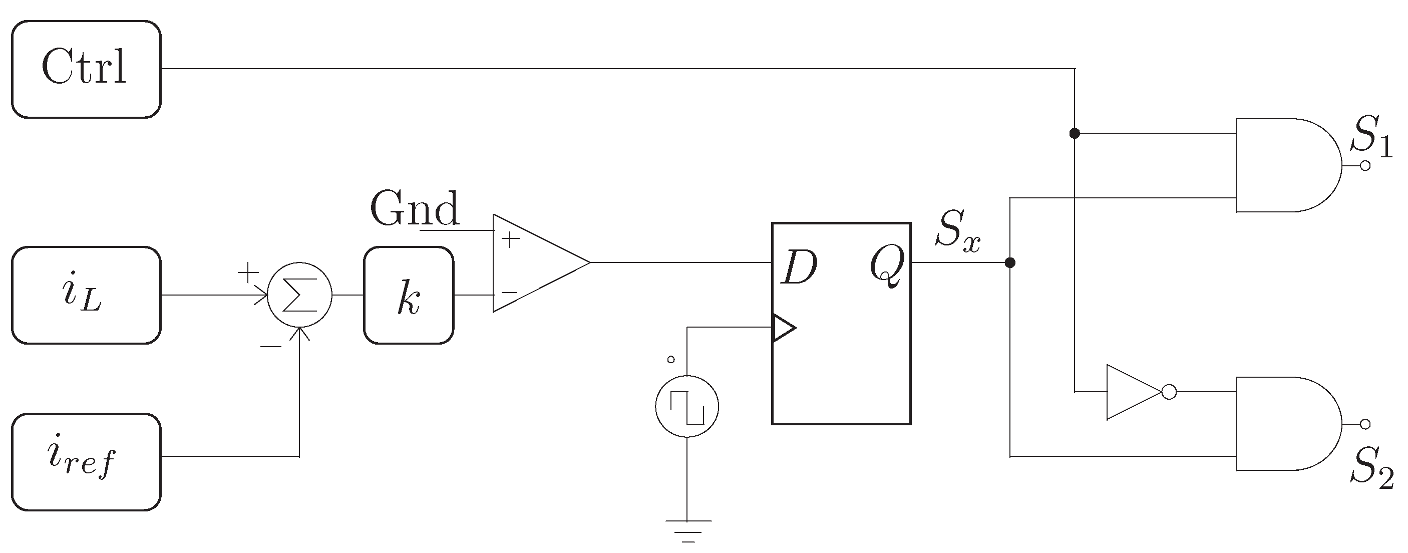
Figure 3 shows the proposed topology for a four-cell battery bank. It is noted that the topology is based on the standard module of the switched-inductor equalizer. Moreover, it has added an array of switches to interconnect this module with the cells to equalize. A key feature of the SPDT switch is that it does not need to work at high speed. Its mission is to connect the points of the circuit so that the transfer of energy between two cells is possible with switches S 1 and S 2 . Therefore, these switches can be implemented with relays. This way, a topology with a reduced component count is achieved. Nevertheless, the equalization time is compromised in this topology since only one inductor handles all energy transfers.
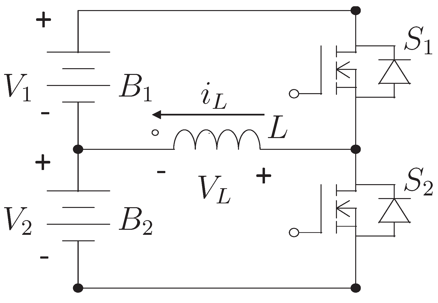
Figure 4 shows the typical module of the switched-inductor equalizer. This circuit consists of two cells, one inductor, and two switches. Only the switch associated with the highest operating voltage cell during a power transfer is activated. The other switch is off during the transfer. For instance, if V 1 > V 2 is required to transfer energy from cell 1 to cell 2, the control is achieved through the switch S 1 . Figure 5 shows the path of the current for both states of the MOSFET S 1 : on and off.
Equation (1) rules the behavior of the current through the inductor in the on state of the switch S 1 . Where i L is the current through the inductor L, V 1 is the voltage in cell 1, and L is the value of the inductance of the inductor. On the other hand, Equation (2) rules the behavior of the current through the inductor in the off state of the switch S 1 . In this case, V 2 is the voltage in cell 2, while the other symbols indicate the same variable indicated in the previous equation.
These are basic equations since both circuits consist of the inductor in shunt with a cell. The difference lies in the off-circuit since the sign convention dictates that the current derivative is negative. Therefore, in this case, the inductor is in discharge mode. Equation (3) is used to model the operation of the circuit. Where X represents the state vector, A 1 represents the state matrix for the on state, A 2 represents the state matrix for the off state, d is the duty cycle of the switch, B 1 represents the input matrix for the on state, B 2 represents the input matrix for the off state, and u is the input of the system. In this case, the state vector is defined by the current through the inductor ( i L ), the A matrixes are considered 0, and u is 1. Therefore, substituting these values leads to Equation (4). This equation represents the averaged model of the module. This model is widely used in power electronics to predict the behavior of a system and to control it [20].
d i L ( t ) d t = V 1 L
d i L ( t ) d t = V 2 L
X ¯ ˙ = [ A 1 d ¯ + A 2 ( 1 d ¯ ) ] X ¯ + [ B 1 d ¯ + B 2 ( 1 d ¯ ) ] u ¯
d i L ¯ ( t ) d t = V 1 ¯ L d ¯ V 2 ¯ L ( 1 d ¯ ) = V 1 ¯ d ¯ V 2 ¯ + V 2 ¯ d ¯ L
Figure 6 shows the behavior and steady-state waveforms of the module. In the first stage, the cell with a higher voltage transfers energy to the inductor by activating the proper switch. Next, the switch is turned off, and the power is transferred from the inductor to the other cell through the diode.
Figure 6 and Equations (1) and (2) help us to conclude that the value of the voltage does not affect the state of charge/discharge of the inductor. However, it does affect the charge/discharge rate. This characteristic is used to propose a single module to handle all the volume of equalization. This strategy requires an array of switches to connect the three terminals of the module to the appropriate nodes in the battery bank. The only constraint for the connection is that the cells/modules must be adjacent since the inductor node must be connected with both cells/modules.
Figure 7 shows the proposed operation of the converter. In the first stage, the voltage of the string made by cells B 1 and B 2 is equalized with the string made by cells B 3 and B 4 . In this case, the switch S P D T 1 is connected to node 1, S P D T 2 to 7 and S P 3 T to 4. Once the strings are equalized, cells B 1 and B 2 are handled. For this purpose, the switch S P D T 1 is connected to node 1, S P D T 2 to 6 and S P 3 T to 3. Finally, it is required to equalize cells B 3 and B 4 . In order to achieve this goal, switch S P D T 1 is connected to node 2, S P D T 2 to 7, and S P 3 T to 5. In this way, the battery bank is completely equalized. It is important to note that in each of these three states, the circuit was operated like the module shown in Figure 4. The cell or module with the highest voltage gives energy to the cell/module with the lowest voltage, activating the proper switch. Moreover, the battery bank equalization is achieved with a reduced component circuit.

3. Design of the Proposed Equalizer

This section provides the guidelines for designing the proposed equalizer. The design process involves the power stage and the controller of the converter. The methodology is proposed for a battery bank of 4 cells such as the one presented in Figure 3. However, it can be extrapolated to any number of cells. Moreover, the cells are considered as 18,650 Li-ion batteries. Figure 8 shows the characteristic curve of these types of cells [21].

3.1. Power Stage Design

The power stage design addresses the sizing of the two MOSFETs, the array of switches, and the inductor. The necessary switches are sized to withstand the current and voltage of the application. Moreover, it is crucial to consider the switching speed desired for the application. A high switching speed is not required in the case of the single pole and double throw and the single pole and triple throw switches; since they will connect the two MOSFETs and the inductor to specific points of the battery bank. This connection will remain until the cells or string of cells are equalized. Therefore, these switches can be implemented with latching relays. The only restriction on their selection is that they must withstand the current of the application. In this case, as 18650 batteries are considered, the maximum current possible is 4 A [1]. However, the MOSFETs must withstand the current of the application and high switching speed. At a higher switching speed, the required inductor can be smaller. In this case, a switching frequency of 100 kHz will be used.
The sizing of the inductor depends on the nominal current, the current ripple, and the desired switching frequency. The switching frequency is chosen as 100 kHz. Furthermore, to achieve a fast process, the nominal current should be as close as possible to the maximum current allowed by the cells. In this case, it was selected at 3.6 A. Finally, the current desired ripple is 0.4 A (approximately 11% of the nominal current). Therefore, ideally, the current will always be between 3.4–3.8 A. Equation (5) describes the behavior of the voltage in an inductor. Where V L is the voltage in the inductor, L is the inductance, and i L is the current through the inductor. Equation (5) yields to (6). In this case, the Δ represents the variation of one variable. Therefore, this equation will be used to obtain the minimum L value to guarantee the desired current ripple. The tension used was 8.4 V since it is the worst scenario that can lead to a greater slope. Moreover, the current variation used was 0.4 A, and finally, the time is the inverse of the frequency established in the frequency limiter (10  μ s). Therefore, it can be seen that the minimum value that guarantees the desired ripple, under the given conditions, is 210 μ H.
V L = L d i L d t
L = V Δ t Δ i L

3.2. Controller Design

The controller needed in this circuit consists of two levels. A low level controller rules the current in the inductor. In this way, the circuit guarantees a safe current for the cells. This controller receives two signals: the measured current and a signal from the high-level controller indicating the switch to operate. In addition, as a part of this low-level design, a sliding mode controller is introduced to rule the current regulation. Starting from Equation (4), the variable d is substituted for u, and it is obtained the following equation.
d i L ¯ ( t ) d t = ( V 1 ¯ + V 2 ¯ ) u V 2 ¯ L
where u is a proposed control signal. Moreover, the sliding surface is proposed as shown in Equation (7). Where σ is the sliding surface, k is a proposed gain, i L is the current through the inductor, and i r e f is the desired current through the inductor.
σ = k ( i L i r e f )
u = 1 ; σ < 0 0 ; σ > 0
Therefore, the derivative of the sliding surface is:
σ ˙ = k ( V 1 ¯ + V 2 ¯ ) u V 2 ¯ L
Finally, it is necessary to check the condition of existence. For this, it is necessary to verify that σ σ ˙ < 0 . If σ > 0 , then u = 0 and σ ˙ must be lower than 0.
σ ˙ = k ( V 1 ¯ + V 2 ¯ ) 0 V 2 ¯ L = k V 2 ¯ L
Therefore, in order to achieve σ ˙ < 0 , k must be greater than 0. Similarly, if σ < 0 , then u = 1 and σ ˙ must be greater than 0.
σ ˙ = k ( V 1 ¯ + V 2 ¯ ) 1 V 2 ¯ L = k V 1 ¯ L
In this case, also k must be greater than 0. Therefore, the sliding mode controller is suitable for this application with a gain (k) greater than 0. Figure 9 shows the implementation of this low-level controller.
In this case, this procedure can be suppressed since it only contains a single variable and, therefore, it is straightforward. Equations (1) and (2) show the behavior of the current in the inductor. Thus, the current in the inductor increases when it is in shunt with the cell with the highest voltage. On the other hand, the current in the inductor decreases in the opposite case. This behavior is used in the low-level controller. The main idea is to keep the switch on while the current is less than a nominal value (3.6 A). When the current exceeds that threshold, the switch must turn off. This controller behavior can lead to a switching speed that can damage the switches. A frequency limiter is introduced at the output of the control signal to avoid this situation. Figure 9 shows this frequency limiter as a type D flip-flop.
On the other hand, the main objective of the high-level controller is to decide the cells or string of cells to equalize. This element is in charge of determining which is the giving and the receiving cell. In addition, it sends a binary signal that indicates to the low-level controller which MOSFET operates. Therefore, the controller requires as input the measurement of the voltage of all the cells in the battery bank. The output is the signal for the latching relays and the signal for the low-level controller. This controller was implemented following a rule-based logic. Appendix A shows the pseudo-code followed by this controller.

4. Comparison

This section aims to clarify the advantages and disadvantages of the proposed topology when comparing it with other BECs. The main points of comparison are current/voltage stress of components, element count, efficiency analysis, equalization time, and controller complexity. Conduction and switching losses are considered to perform the efficiency analysis. The conduction losses are associated with the series resistances of all the elements of the current path. On the other hand, the switching losses are due to the power lost in the switches in the transition time in which they change state.
In this circuit, it can be seen that for any current path, the following elements are touched: a battery cell, two slow commutation switches, a MOSFET, and an inductor. Therefore, Equation (8) rules the behavior of conduction losses. Where i L is the current in the inductor, D is the duty cycle of the PWM signal of the MOSFETs, R o n _ B x is the series resistance of the cell x, R o n _ S P D T x is the series resistance of the S P D T x switch, R L is the series resistance of the inductor and R o n _ S P 3 T is the series resistance of the single pole triple throw switch. Suppose all the cells of the battery bank and the MOSFETs present a similar series resistance. In addition, the single pole triple throw breaker can be implemented with single pole double throw switches, as shown in Figure 10. It yields to Equation (9).
P L _ C o n d = i L 2 ( D ( R o n _ B 1 + R o n _ S P D T 1 + R o n _ S 1 + R L + R o n _ S P 3 T ) + ( 1 D ) ( R o n _ B 2 + R o n _ S P D T 2 + R o n _ S 2 + R L + R o n _ S P 3 T )
P L _ C o n d = i L 2 ( D ( R o n _ B + R o n _ S P D T + R o n _ S + R L + 2 R o n _ S P D T ) + ( 1 D ) ( R o n _ B + R o n _ S P D T + R o n _ S + R L + 2 R o n _ S P D T )
P L _ C o n d = i L 2 ( R o n _ B + R o n _ S + R L + 3 R o n _ S P D T )
Equation (10) shows the equation that rules the switching power losses. Where V x is the voltage applied to the switch, i L is the current through the inductor, f s w is the switching frequency, t r is the time it takes for the switch to change from off to on state, and t f is the time it takes for the switch to change from on to off state. Therefore, the general losses in the converter are the sum of these two components as shown in the Equation (11).
P L _ S w = V x i L f s w ( t r + t f )
P T o t a l = P L _ C o n d + P L _ S w = i L 2 ( R o n _ B + R o n _ S + R L + 3 R o n _ S P D T ) + V x i L f s w ( t r + t f )
Typical values will be used to estimate the power lost in a transfer. The equalization current can be considered 3.5 A since the maximum current in 18,650 cells is 4 A. Furthermore, the maximum series resistance of 18,650 cells reported is 50 mΩ, the drain-source on-resistance of a MOSFET can be taken from 32 mΩ, and the series resistance of a relay (srd -05vdc-sl-c) is 60 mΩ. On the other hand, the resistance in the inductor depends on its construction, cable length, core shape, etc. However, for the present analysis, we will use 75 mΩ. Moreover, the value of the voltage used is 8.4 V, which is the worst case when two cells are fully charged and in shunt with the inductor. Finally, the t r was taken from 60 ns, the t f 45 ns and the f s w as 100 kHz. Therefore, the total power loss is 4.4387 W for these conditions.
Figure 2 shows the main inductor-based cell equalizers. We can use the previous procedure to obtain the power loss equation for these topologies. Equation (12) shows the power loss for the switched inductor equalizer. Where i 1 is the current in the inductor L 1 , R o n _ B is the series resistance of any cell, R o n _ S is the series resistance of any MOSFET, R L 1 is the series resistance of the inductor L 1 , V 1 is the voltage in cell 1, f s w is the switching frequency, t r is the rise time of the MOSFET, and t f is the fall time of the MOSFET. Some assumptions are made to get this equation: the current in all three inductors has the same value, the voltage in all the cells is the same, and the on resistance in all the similar elements is the same. If the values considered above are used, a power loss of 6.2284 W is obtained.
P L _ S w i t c h e d = 3 i 1 2 ( R o n _ B + R o n _ S + R L 1 ) + 3 V 1 i 1 f s w ( t r + t f )
On the other hand, Equation (13) shows the power loss for the inductor-based layer equalizer. Where i 1 is the current in the inductor L 1 , R o n _ B 1 is the series resistance of cell 1, R o n _ S 1 is the series resistance of MOSFET S 1 , R L 1 is the series resistance of the inductor L 1 , V 1 is the voltage in cell 1, f s w is the switching frequency, t r is the rise time of the MOSFET, t f is the fall time of the MOSFET, i 3 is the current in the inductor L 3 , R o n _ S 5 is the series resistance of MOSFET S 5 , and R L 3 is the series resistance of the inductor L 3 . This leads to a power loss of 6.9948 W. Finally, Equation (14) shows the power loss in the equalizer of a single inductor. If a 32 mΩ resistor is used as the value for the on-resistance of the diode, a power loss of 2.468 W is obtained. It can be appreciated that the architectures with less power loss use only one inductor. This is mainly because they use fewer devices and, therefore, the conduction losses are lower. However, these topologies have the disadvantage of taking longer to equalize the battery bank.
P L _ L a y e r = 2 i 1 2 ( R o n _ B 1 + R o n _ S 1 + R L 1 ) + 2 V 1 i 1 f s w ( t r + t f ) + i 3 2 ( 2 R o n _ B 1 + R o n _ S 5 + R L 3 ) + 2 V 1 i 3 f s w ( t r + t f )
P L _ S g l L = i L 2 ( R o n _ B 1 + R o n _ D 1 + R o n _ S 1 + R L ) + V 1 i L f s w ( t r + t f )
Another relevant variable that can be obtained to compare these circuits is efficiency. The efficiency is obtained by means of Equation (15). Where η is the efficiency, V i n is the voltage of the cell that delivers energy in a transfer, I i n is the current through the cell that delivers energy, and P T o t a l is the total of power loss. Considering the values used previously, where the current was 3.5 A and the voltage in the cell is 4.2 V, Table 1 summarizes the efficiency results for each architecture. It can be seen that all topologies work at a similar efficiency, except for the layer of inductors equalizer, as this one is a bit more efficient than the rest.
η = V i n I i n P T o t a l V i n I i n
The proposed equalizer is compared with the schemes of Figure 2. This comparison will be based on the assumption of a four-cell battery bank. It can be seen that the proposed equalizer only has one inductor, while the equalizers present in the literature can have one or three inductors. Furthermore, the proposed equalizer only requires two MOSFETs, while the other circuits require six to ten MOSFETs. However, the proposed topology requires two SPDTs and one SP3T, but these are slow switches that can be implemented with latching relays. These devices are inexpensive and do not require a complex driver.
Considering the stress in the components, in all topologies, the current through the elements is controlled and depends on the reference. However, this does not happen with the voltage, where the equalizer proposed in the worst case must handle a voltage of half the battery bank. This is also the worst case in the layer equalizer. On the other hand, the switched-inductor topology handles a maximum voltage of one cell of the battery bank. Finally, the single-inductor topology depends on how it is operated: cell-to-cell, string-to-string, pack-to-cell, etc. This architecture is very flexible and can handle voltages from a single cell to the entire battery bank.
In general, the proposed topology has a low element count since it only requires one inductor and two MOSFETs for the equalization process. Moreover, it can operate string-to-string or cell-to-cell. Nevertheless, since it only has one inductor to handle all the necessary transfers, the equalization process will take longer. Table 2 summarizes the comparison between these circuits.
So far in this manuscript, the case of foue cells has been analyzed. In addition, this case study will continue to be used in the results of the next section. However, we want to explore what happens in larger battery banks since they are more common. Table 3 shows the component count by topology for battery banks of different sizes. This table shows the small number of components necessary to implement the proposed equalizer. Herein lies the great advantage of this architecture. In addition, it is essential to highlight that as part of the components needed for the realization of the switch network, the functional elements were considered: SPDT, SP4T, SP8T, etc. However, this network can be made with other devices, such as MOSFETs or relays. The selection of the devices to implement the switch network depends on access to any of the mentioned devices.

5. Simulation Results

This section shows the simulation results that validate the equalizer proposed in the present work. This work used the software PSIM, an electronic circuit simulation package explicitly designed for its use in power electronics. Table 4 shows the values used in the simulations.
Figure 11 shows the simulation results for a four-cell battery bank equalization process. The expected outcome can be seen; first, cells 1 and 2 are equalized, then cells 3 and 4, and finally, the two halves of the battery bank are equalized. On the other hand, it can be seen that the current is as close as possible to 4 A without exceeding this threshold. This current is desired to have a process as fast as possible. In addition, it is safe for the cells since the maximum allowed current is not exceeded. Figure 12 shows a close-up of the current through the inductor to better appreciate the ripple. It can be seen that the designed ripple is achieved (0.4 A). Finally, it can be seen that cells 2 and 3 gave away the electrical charge (a total of 10.52 mAh between both) to cells 1 and 4. This behavior is expected since the voltage in the cells is proportional to the electric charge they present.
Figure 13 shows the drain-source voltage stress on the switch S 1 ( V D S 1 ). It can be seen that it is approximately twice the voltage of the cells that are being equalized. At first, when only individual cells are equalized, it presents a voltage of about 8 V. Whereas, when both halves of the battery bank are equalized, it has an approximate voltage of 16 V. This is expected since the inductor is charged at the same voltage as the cells that are being equalized. Therefore, twice the voltage of the cells being equalized is reflected in the switch. Moreover, the current stress in the switch is the current through the inductor since these elements are in series.
Additionally, an experiment was performed to verify that the equalizer worked while the battery bank delivered power to the propulsion system. Figure 14 shows the simulation of the equalization process when connecting a load to the battery bank. The following data was taken as initial condition: V 1 = 4.45 V, V 2 = 3.9 V, V 3 = 4.55 V, and V 4 = 4.75 V. In addition, the current reference was 5 A for the inductor, and the current that was put into the load was 2 A, with a frequency of 10 kHz, as can be seen in Figure 15. In real-life scenarios, this is not a typical current pattern. However, it is a way to evaluate the behavior of the system when it faces sudden changes in current. In this figure, the equalization process was not affected by the load, which is desirable since waiting for the car to be parked to equalize the battery bank is not necessary.
Finally, we performed simulations with the same conditions as those carried out in work [8]. Figure 16 show the results for those conditions. Therefore, the metrics from that work can be used to compare the proposed converter, as showed in Table 5. An inductor, two MOSFETs, and five SPDT switches are required in the proposed converter. In addition, it requires a low-level current controller, a high-level controller to make decisions, and four voltage sensors and a current sensor. Finally, it was obtained that the equalization time was 22 s, and it was evidenced a voltage and current stress in the MOSFETs of 16 V and 4 A, respectively. Therefore, it can be concluded that the proposed equalizer is the second circuit with fewer elements (only behind the shunt-MOSFET topology). Moreover, it has a competitive equalization time (since the current is controlled to a value as close as possible to the maximum allowed current). The switches present similar stress to other topologies. However, it is more complex to control and requires several sensors. Therefore, we think this is an exciting topology, and it can complement existing equalizers.

6. Conclusions

A novel equalizer based on a single inductor was proposed for its application in EVs in this work. A topology was achieved that only requires an inductor and two MOSFETs; therefore, it presents a low element count. In addition, a fast equalization process is performed. This speed is explained because the inductor controls the current to values as close as possible to the maximum current allowed by the cells. This converter can be used for power transfers between adjacent cells and string-to-string. Finally, it was compared with other equalizers present in the literature, taking into account the number of components, equalization time, stress on the MOSFETs, number of sensors, and complexity of the controller.
This paper gives the guidelines for the analysis of the operation and design of the proposed equalizer. The module of the switched-inductor architecture was analyzed, which served as the basis for the proposed converter. The controller was divided into two subsystems: a low-level current controller and a high-level controller in charge of deciding the source and destination cell for each energy transfer. The PSIM software was used to validate the theoretical analysis. The simulations showed the correct operation of the proposed equalizer. In addition, the equalization time, the ripple of the current, and the stress in the MOSFETs of the converter were analyzed. Overall, this converter has proven to be a viable, low-cost option for cell equalization in an EV battery bank.

Author Contributions

Conceptualization, A.A.-D. and J.R.-R.; methodology, R.V.C.-S. and J.R.-R.; software, A.A.-D.; validation, A.A.-D. and R.V.C.-S.; formal analysis, J.R.-R.; investigation, A.A.-D.; resources, J.R.-R. and R.V.C.-S.; data curation, A.A.-D. and J.R.-R.; writing—original draft preparation, review, and editing, A.A.-D., J.R.-R. and R.V.C.-S. All authors have read and agreed to the published version of the manuscript.

Funding

This research was funded by the National Council on Science and Technology and FOPER under grant FIN02455.

Conflicts of Interest

The authors declare no conflict of interest.

Abbreviations

    The following abbreviations are used in this manuscript:
EVElectric vehicle
BECBattery equalizer circuit

Appendix A

Algorithm A1:
Batteries 09 00065 i001

References

  1. Alvarez-Diazcomas, A.; López, H.; Carrillo-Serrano, R.V.; Rodríguez-Reséndiz, J.; Vázquez, N.; Herrera-Ruiz, G. A novel integrated topology to interface electric vehicles and renewable energies with the grid. Energies 2019, 12, 4091. [Google Scholar] [CrossRef] [Green Version]
  2. Kurz, L.; Faryadras, M.; Klugius, I.; Reichert, F.; Scheibe, A.; Schmidt, M.; Wörner, R. Global Warming Potential of a New Waterjet-Based Recycling Process for Cathode Materials of Lithium-Ion Batteries. Batteries 2021, 7, 29. [Google Scholar] [CrossRef]
  3. Jenn, A.; Springel, K.; Gopal, A.R. Effectiveness of electric vehicle incentives in the United States. Energy Policy 2018, 119, 349–356. [Google Scholar] [CrossRef]
  4. Williamson, S.S.; Rathore, A.K.; Musavi, F. Industrial electronics for electric transportation: Current state-of-the-art and future challenges. IEEE Trans. Ind. Electron. 2015, 62, 3021–3032. [Google Scholar] [CrossRef]
  5. Khaligh, A.; D’Antonio, M. Global trends in high-power on-board chargers for electric vehicles. IEEE Trans. Veh. Technol. 2019, 68, 3306–3324. [Google Scholar] [CrossRef]
  6. Tudoroiu, R.E.; Zaheeruddin, M.; Tudoroiu, N.; Radu, S.M. SOC Estimation of a Rechargeable Li-Ion Battery Used in Fuel-Cell Hybrid Electric Vehicles—Comparative Study of Accuracy and Robustness Performance Based on Statistical Criteria. Part I: Equivalent Models. Batteries 2020, 6, 42. [Google Scholar] [CrossRef]
  7. Hoque, M.; Hannan, M.; Mohamed, A.; Ayob, A. Battery charge equalization controller in electric vehicle applications: A review. Renew. Sustain. Energy Rev. 2017, 75, 1363–1385. [Google Scholar] [CrossRef]
  8. Alvarez-Diazcomas, A.; Estévez-Bén, A.A.; Rodríguez-Reséndiz, J.; Martínez-Prado, M.A.; Carrillo-Serrano, R.V.; Thenozhi, S. A Review of Battery Equalizer Circuits for Electric Vehicle Applications. Energies 2020, 13, 5688. [Google Scholar] [CrossRef]
  9. Carter, J.; Fan, Z.; Cao, J. Cell equalisation circuits: A review. J. Power Sources 2020, 448, 227489. [Google Scholar] [CrossRef]
  10. Ali, M.U.; Zafar, A.; Nengroo, S.H.; Hussain, S.; Junaid Alvi, M.; Kim, H.J. Towards a smarter battery management system for electric vehicle applications: A critical review of lithium-ion battery state of charge estimation. Energies 2019, 12, 446. [Google Scholar] [CrossRef]
  11. Mubenga, N.S.; Sharma, K.; Stuart, T. A Bilevel Equalizer to Boost the Capacity of Second Life Li Ion Batteries. Batteries 2019, 5, 55. [Google Scholar] [CrossRef] [Green Version]
  12. Moo, C.; Hsieh, Y.; Tsai, I.; Cheng, J. Dynamic charge equalisation for series-connected batteries. IEEE Proc. Electr. Power Appl. 2003, 150, 501–505. [Google Scholar] [CrossRef] [Green Version]
  13. Phung, T.H.; Crebier, J.C.; Chureau, A.; Collet, A.; Nguyen, V. Optimized structure for next-to-next balancing of series-connected lithium-ion cells. In Proceedings of the 2011 Twenty-Sixth Annual IEEE Applied Power Electronics Conference and Exposition (APEC), Fort Worth, TX, USA, 6–11 March 2011; pp. 1374–1381. [Google Scholar]
  14. Yarlagadda, S.; Hartley, T.T.; Husain, I. A battery management system using an active charge equalization technique based on a DC/DC converter topology. IEEE Trans. Ind. Appl. 2013, 49, 2720–2729. [Google Scholar] [CrossRef]
  15. Peng, F.; Wang, H.; Yu, L. A hierarchical ZVS battery equalizer based on bipolar CCM buck-boost units. In Proceedings of the 2018 IEEE Energy Conversion Congress and Exposition (ECCE), Portland, OR, USA, 23–27 September 2018; pp. 2120–2126. [Google Scholar]
  16. Guo, X.; Kang, L.; Huang, Z.; Yao, Y.; Yang, H. Research on a novel power inductor-based bidirectional lossless equalization circuit for series-connected battery packs. Energies 2015, 8, 5555–5576. [Google Scholar] [CrossRef] [Green Version]
  17. Hsieh, Y.C.; Moo, C.S.; Tsai, I.; Cheng, J.C. Dynamic charge equalization for series-connected batteries. In Proceedings of the 2002 IEEE International Conference on Industrial Technology, Bankok, Thailand, 11–14 December 2002; Volume 1, pp. 444–449. [Google Scholar]
  18. Shang, Y.; Zhang, Q.; Cui, N.; Zhang, C. A cell-to-cell equalizer based on three-resonant-state switched-capacitor converters for series-connected battery strings. Energies 2017, 10, 206. [Google Scholar] [CrossRef]
  19. Moghaddam, A.F.; Van den Bossche, A. A battery equalization technique based on Ćuk converter balancing for lithium ion batteries. In Proceedings of the 2019 8th International Conference on Modern Circuits and Systems Technologies (MOCAST), Thessaloniki, Greece, 13–15 May 2019; pp. 1–4. [Google Scholar]
  20. Ang, S.; Oliva, A.; Griffiths, G.; Harrison, R. Power-Switching Converters; CRC Press: Boca Raton, FL, USA, 2010. [Google Scholar]
  21. Novak, M.; Chysky, J.; Novak, L. Data from long time testing of 18650 lithium polymer batteries. Data Brief 2020, 29, 105137. [Google Scholar] [CrossRef] [PubMed]
  22. Kim, M.Y.; Kim, J.W.; Kim, C.H.; Cho, S.Y.; Moon, G.W. Automatic charge equalization circuit based on regulated voltage source for series connected lithium-ion batteries. In Proceedings of the 8th International Conference on Power Electronics-ECCE Asia, Jeju, Republic of Korea, 30 May–3 June 2011; pp. 2248–2255. [Google Scholar]
  23. Goodarzi, S.; Beiranvand, R.; Mousavi, S.M.; Mohamadian, M. A new algorithm for increasing balancing speed of switched-capacitor lithium-ion battery cell equalizers. In Proceedings of the 6th Power Electronics, Drive Systems & Technologies Conference (PEDSTC2015), Tehran, Iran, 3–4 February 2015; pp. 292–297. [Google Scholar]
Figure 1. Classification of the BECs.
Batteries 09 00065 g001
Figure 2. Classic architectures of BECs based on inductors, (a) switched-inductor topology, (b) layer topology, (c) single-inductor topology.
Batteries 09 00065 g002
Figure 3. Proposed single-inductor battery equalizer.
Batteries 09 00065 g003
Figure 4. Module of the switched-inductor scheme applied to a two-cells battery bank.
Batteries 09 00065 g004
Figure 5. Operation of the module of the switched-inductor architecture, (a) on-state, (b) off-state.
Batteries 09 00065 g005
Figure 6. Waveform of the module of the switched-inductor topology.
Batteries 09 00065 g006
Figure 7. Operation of the proposed topology.
Batteries 09 00065 g007
Figure 8. Characteristic curve of the 18,650 battery.
Batteries 09 00065 g008
Figure 9. Low-level current controller.
Batteries 09 00065 g009
Figure 10. Implementation of a SP3T switch based on SPDT switches.
Batteries 09 00065 g010
Figure 11. Equalization of a four-cell battery bank using the proposed equalizer.
Batteries 09 00065 g011
Figure 12. Zoom of the current trough inductor.
Batteries 09 00065 g012
Figure 13. Voltage in the switch S 1 through the equalization process.
Batteries 09 00065 g013
Figure 14. Simulation of the equalization process when a load is connected to the battery bank.
Batteries 09 00065 g014
Figure 15. Zoom of the current pattern connected to the battery bank.
Batteries 09 00065 g015
Figure 16. Simulation results for the equalization process with the same conditions of the work [8].
Batteries 09 00065 g016
Table 1. Summary of the values of efficiency obtained for each architecture.
SchemeEfficiency [%]
Switched-inductor85.87
Layer of inductors88.1
Single-inductor83.21
Proposed equalizer84.9
Table 2. Comparative analysis of the inductor-based BECs.
EqualizerComponents for n CellsPower Losses for 4 Cells TopologyRemarks
Switched-inductor topology [9] n 1 inductors6.2284 WIt is the classical topology, and its module is the base for other schemes. It can only transfer energy between adjacent cells. In addition, it features several inductors that are heavy, bulky, and expensive elements.
2 ( n 1 ) MOSFETs
Layer topology [22] n 2 + n 4 + n 8 inductors6.9948 WIt is based on the switched-inductor equalizer module. In addition, it allows string-to-string transfer. However, it has several inductors.
2 ( n 2 + n 4 + n 8 ) MOSFETs
Single-inductor topology [23]1 inductor2.468 WIt only requires one inductor. In addition, it is very flexible, allowing several possible transfers: direct cell-to-cell, cell-to-pack, pack-to-cell, etc. However, to take advantage of these transfers requires a complex controller. Finally, the equalization process is slow.
2 ( n + 1 ) MOSFETs
2 ( n + 1 ) diodes
Proposed equalizer1 inductor4.4387 WIt requires one inductor and two fast-speed switches. So it is a cheap and easy-to-control circuit as it is based on a well-known module. In addition, it requires switches to connect the module nodes to the battery bank. However, these devices are inexpensive and need a simple driver.
2 MOSFETs
2 ( n 2 1 ) + n 1 SPDT
Table 3. Component count considering the number of cells in the battery bank.
Equalizer4 Cells8 Cells16 Cells32 Cells
Switched-inductor topology [9]3 inductors7 inductors15 inductors31 inductors
6 MOSFETs14 MOSFETs30 MOSFETs62 MOSFETs
Layer topology [22]3 inductors7 inductors15 inductors31 inductors
6 MOSFETs14 MOSFETs30 MOSFETs62 MOSFETs
Single-inductor topology [23]1 inductor1 inductor1 inductor1 inductor
10 MOSFETs18 MOSFETs34 MOSFETs66 MOSFETs
10 diodes18 diodes34 diodes66 diodes
Proposed equalizer1 inductor1 inductor1 inductor1 inductor
2 MOSFETs2 MOSFETs2 MOSFETs2 MOSFETs
2 SPDTs2 SP4Ts2 SP8Ts2 SP16Ts
1 SP4T1 SP8T1 SP16T1 SP32T
Table 4. Value of the components used in the simulation.
ComponentValue
Battery cellQ = 2500 mAh, I m a x = 4 A
Initial voltages V 1 = 4.01 V , V 2 = 4.1 V
V 3 = 4.08 V , V 4 = 4.06 V
Inductor210 μ H
Table 5. Comparative analysis of the reviewed equalizers for a four-cell battery bank [8].
EqualizerComponent CountEqualization Time [s]MOSFET StressHigh-Level Controller ComplexitySensors RequiredEfficiency
Switched-inductor topology [9]6 MOSFETs, 3 inductors164.2 V, 3.8 ALow4 (V), 3 (A)85.87%
Layer of inductors topology [9]6 MOSFETs, 3 inductors158.4 V, 3.8 ALow4 (V), 3 (A)88.1%
Single-inductor topology [23]10 MOSFETs, 10 diodes
1 inductor
234.2 V, 3.8 AHigh4 (V), 1 (A)83.21%
Proposed equalizer2 MOSFETs, 5 SPDTs
1 inductor
228.4 V, 3.8 AHigh4 (V), 1 (A)84.9%
Disclaimer/Publisher’s Note: The statements, opinions and data contained in all publications are solely those of the individual author(s) and contributor(s) and not of MDPI and/or the editor(s). MDPI and/or the editor(s) disclaim responsibility for any injury to people or property resulting from any ideas, methods, instructions or products referred to in the content.

