Article

CVD Graphene Electrode for Direct Electrochemical Detection of Double-Stranded DNA

1
Research and Technology Center of Energy, Laboratory of Nanomaterials and Renewable Energy Systems, Borj-Cedria Science and Technology Park, BP 95, Hammam-Lif 2050, Tunisia
2
Biomedical Genomics and Oncogenetics Laboratory, Institut Pasteur de Tunis, University Tunis El Manar, Tunis 1068, Tunisia
3
Center of Physics and Engineering of Advanced Materials, Laboratory for Physics of Materials and Emerging Technologies, Chemical Engineering Department, Instituto Superior Técnico, Universidade de Lisboa, 1049-001 Lisbon, Portugal
*
Authors to whom correspondence should be addressed.
Inorganics 2023, 11(4), 173; https://doi.org/10.3390/inorganics11040173
Submission received: 21 January 2023 / Revised: 14 April 2023 / Accepted: 18 April 2023 / Published: 20 April 2023
(This article belongs to the Special Issue Electrochemical Study of Nanocarbon Based Materials)

Abstract

:
Understanding and regulating DNA interactions with solvents and redox-active centers opens up new possibilities for improving electrochemical signals and developing adequate biosensors. This work reports the development of a modified indium tin oxide (ITO) electrode by chemical vapor deposition (CVD) of graphene for the detection of double-stranded DNA. The modified electrode shows a better electrical conductivity than ITO, as confirmed by electrochemical impedance spectroscopy (EIS), where a drastic decrease in the charge–transfer resistance, Rct, from ~320 to ~60 Ω was observed. Sequences of double-stranded genomic DNA with a different number of base pairs are evaluated through differential pulse voltammetry (DPV), using ferri/ferrocyanide ([Fe(CN)6]3−/4−) as a mediator in the solution. Variations in the electrochemical response of the [Fe(CN)6]3−/4− probe are observed after introducing redox inactive double-stranded DNA ions. The redox-active [Fe(CN)6]3−/4− probe serves as a scaffold to bring DNA into the graphene-modified ITO electrode surface, provoking an increase in the current and a change in the potential when the number of base pairs increases. These results are confirmed by EIS, which shows a variation in the Rct. The calibration of DPV intensity and Rct vs. DNA base pairs (bps) number were linear in the 495–607 bps range. The proposed method could replace the nucleic acid gel electrophoresis technique to determine the presence of a DNA fragment and quantify its size.

Graphical Abstract

1. Introduction

In the framework of the development and application of advanced materials, increasing attention was devoted to 2D materials, especially to graphene, thanks to its distinctive band structure and extraordinary physical properties: strong mechanical strength, lightness, flexibility, stable chemical properties, impermeability, excellent thermal, and electrical conductivity [1,2,3,4]. In fact, since the discovery of the first mechanically exfoliated graphene layers, by Geim and coworkers [5], many research groups have been competing in using graphene and its derivatives for a wide range of applications such as in electronics, in the food industry, for energy storage, and in the biotechnology field [6,7,8,9,10,11,12]. In particular, graphene is considered a versatile transducing material due to its high specific surface area, high mechanical adhesion, rapid electron transfer, low noise, chemical stability, and corrosion resistance. A wide variety of research works have been carried out to produce efficient graphene-based sensors with excellent transducing properties [13,14,15,16].
Many approaches are used to synthesize graphene, including epitaxial growth on silicon carbide and chemical exfoliation of graphene sheets [17,18]. However, the key point remains the synthesis of large-domain graphene for large-scale graphene device integration. In 2009, Li et al. proposed the chemical vapor deposition (CVD) of graphene on centimeter-scale copper substrates, paving the way for the large-scale manufacture of high-quality graphene sheets for various industrial uses [19]. Today, wide and flexible copper foil substrates are rolled and inserted inside a tubular furnace to obtain large surfaces and homogeneous graphene films [20,21]. To achieve large-area uniform graphene films, it is essential to monitor the different growth parameters [22]. For example, a long enough annealing time of copper foils at atmospheric pressure reduces nucleation density to achieve up to 1.3 mm large graphene domains. Large graphene domains are indeed crucial, especially for sensing applications.
Graphene biosensors are extremely valuable in molecular biology, medicine, or even clinical practices as they can considerably improve patient care and contribute to the early diagnosis of diseases. So far, innovative sensing systems have been presented using graphene electrodes associated with diseases nanoparticles or polymers [23]. These systems are based on immobilizing biomolecules, such as enzymes, antibodies, and DNA, to design biosensors with high sensitivity and selectivity [24,25]. In most biosensors, the graphene surface has to be changed by covalent or non-covalent bindings to create an interaction with the recognition molecule. This process has to be simple, fast, and reproducible.
Multiple detection techniques are employed. Commonly, graphene field-effect transistors (G-FET) are used. They are made using a multi-step manufacturing process, including a lithographic process. These procedures tend to introduce contamination onto the graphene surface, which may cause an interference for subsequent biosensing [26,27,28]. One alternative sensing technique is the electrochemical method [29,30,31]. The significant characteristics of this method are its simplicity, efficiency, and excellent sensitivity. In fact, an electrochemical biosensor is a system that provides exact quantitative analytical data by combining biological recognition components with an electrochemical transduction element. In electrochemical biosensing, several techniques are used. Among them, potentiometry, amperometry, and conductimetry are frequently employed. Nevertheless, amperometric biosensors have the most significant commercial success and have shown their efficiency and extreme sensitivity for the detection of DNA. For instance, several research groups have developed amperometric genosensors for rapid, specific, and sensitive detection of DNA [32,33]. Multiple electrochemical biosensors are also developed using graphene and carbon-based materials.
In most graphene-based electrochemical biosensors, graphene oxide (GO) and reduced graphene oxide (rGO) are used [34,35,36]. For example, Xu et al. have proposed a highly sensitive electrochemical biosensor of target DNA using an rGO electrode with exonuclease III as a driving force and tetraferrocene as a signal indicator [35]. Although rGO has improved conductivity compared to graphene oxide (GO), some remaining oxygen groups may still be present after the reduction reaction. A GO and polyaniline nanowires (PANIws) based DNA biosensor was also developed by Bo et al. [34]. Using differential pulse voltammetry (DPV), the obtained graphene/PANIw functionalized glassy carbon electrode (GCE) showed an improved current response for DNA sequences [36]. The functional groups and the graphene’s oxidation states may strongly affect the sensor response and the bonding between the transducer and bioreceptor. The number of functional groups can also influence the target molecule’s interactions and detection limit [37].
On the other hand, most electrochemical DNA sensors have focused on detecting hybridization events using the immobilization of single-stranded DNA (ssDNA). Recently, a new addressable approach to immobilizing ssDNA has been developed. Its technology relies on the Michael addition reaction of thiolated (ssDNA) to the form of oxidation of benzoquinone [38,39]. Nevertheless, understanding DNA double helix–electron transfer seems very interesting as it provides a sensitive tool to detect the potential damage in the genome [40]. The DNA is frequently tagged with a redox-active probe molecule (ferrocene or quinone) [41,42]. Alternatively, DNA sensors may exploit non-covalent electrostatic interactions between the negatively charged DNA backbone and redox-active cations such as Ru(NH3)63+ [43,44]. Few works have been reported on the detection of double-stranded DNA employing electrochemical detection [45,46,47,48,49].
Dubuisson et al. have proposed an anodized epitaxial graphene electrode with excellent performances for electrochemical impedance spectroscopy (EIS) as well as differential pulse voltammetry detection of immobilized DNA and free DNA. They have assessed the anodized platform’s sensitivity and chemical resistance for biosensing at the solution–electrode interface. They have also investigated the frequency-dependent impedimetric response of the anodized surfaces modified with DNA [47]. Benvidi et al. have created label-free DNA biosensors based on modified GCEs with rGO and carbon nanotubes (MWCNTs) for identifying DNA sequences. Using cyclic voltammetry (CV) and EIS, they carried out the immobilization of the probe and its hybridization with the target DNA under ideal conditions [48].
In the present work, the electrochemical signal of ferri/ferrocyanide ([Fe(CN)6]3−/4−) in solution is exploited as a mediator to measure the signal difference of double-stranded DNA and to differentiate between DNA fragment sizes by means of DPV using a CVD graphene electrode. Using such an approach will open new opportunities for developing electrochemically based techniques that could take the place of nucleic acid gel electrophoresis, which is the established method in molecular biology for determining the presence of a DNA fragment and its general size using a DNA marker. To the best of the authors’ knowledge, this work reports for the first time a platform based on a graphene electrode that distinguishes between various sequences of double-stranded genomic DNA in terms of their number of base pairs. This platform is used to overcome the drawback of the electrophoresis technique that requires a lot of time to prepare the electrophoresis gel and to carefully incorporate the Polymerase Chain Reaction (PCR) products into the gel.

2. Results and Discussion

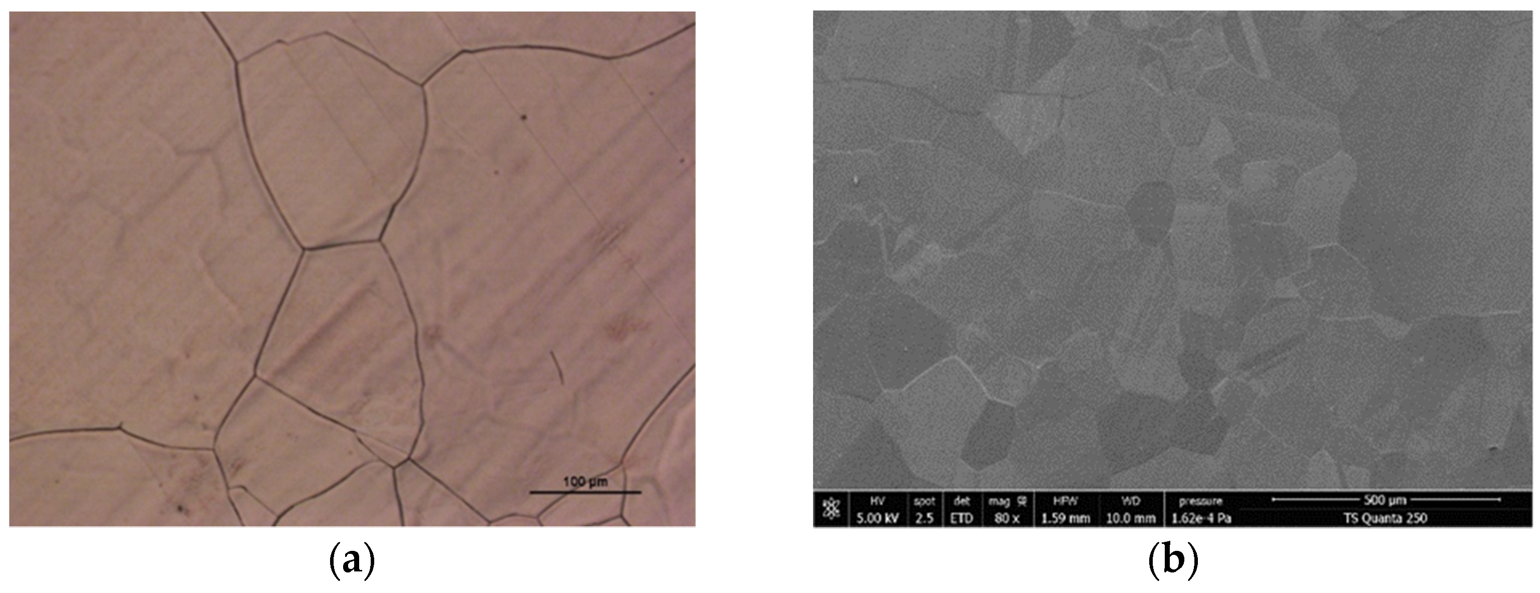
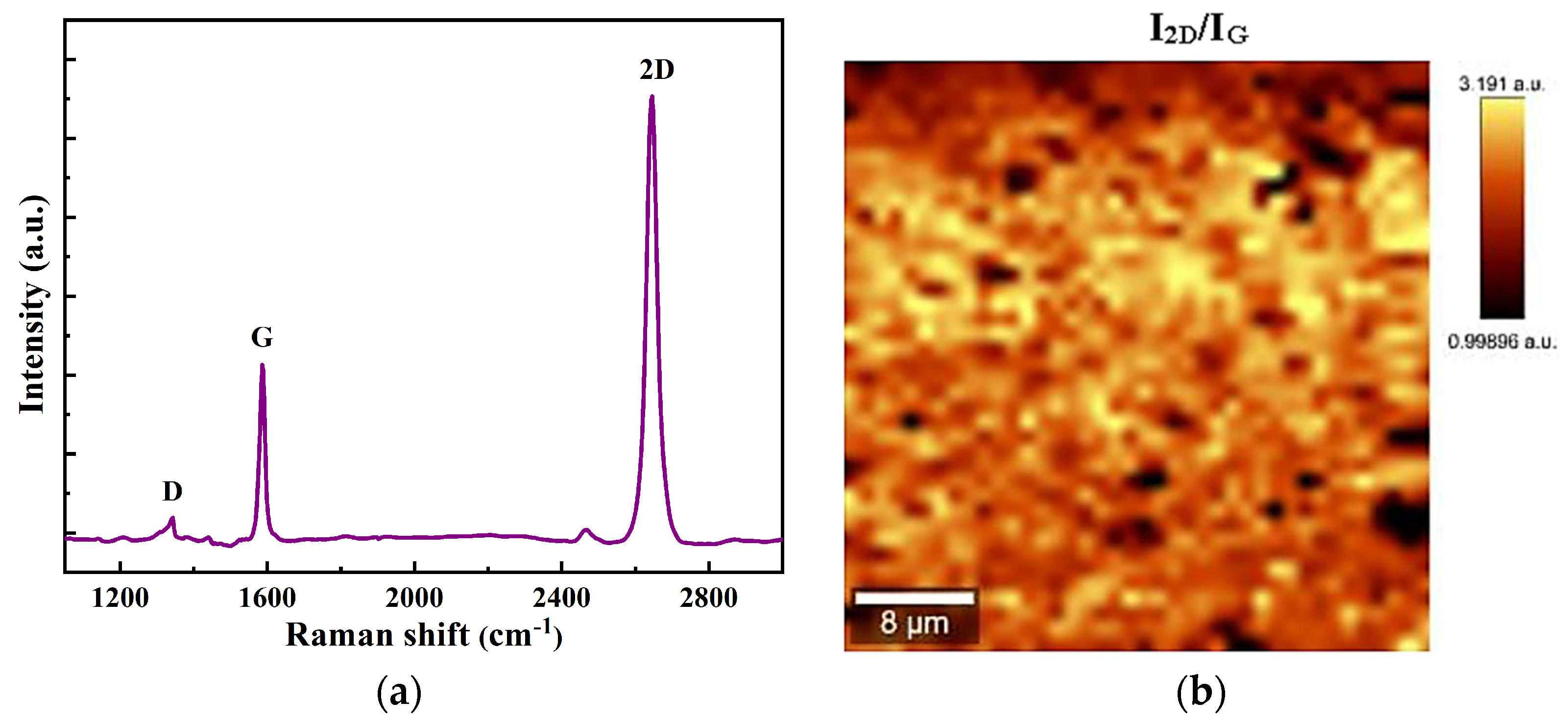
2.1. Characterization of the Graphene Layer

To identify the size and shape of the graphene flakes on the copper foil, the graphene/copper sample is initially oxidized in the air using the revealed graphene visualization method [50,51], producing a reflecting contrast between the oxidized copper in the exposed portions and the unexposed copper covered by graphene. This technique gives us a first idea of the quality of the grown graphene. The surface of the graphene/copper foil is then analyzed using an optical microscope and a scanning electron microscope (SEM). Figure 1a shows a 20-times magnification optical micrograph of the sample. A few areas of copper oxide (dark red areas) confirm that graphene is fully grown on the entire surface. In Figure 1b, the SEM image of graphene/copper foil reveals a continuous film with an average grain size of 150 µm. Several graphene domains can be observed with different contrasts indicating that some areas might be multi-layer graphene.
Raman spectroscopy is then used to evaluate the uniformity and quality of the synthesized graphene on a silicon oxide (SiO2) substrate. At the Brillouin zone center, Γ, graphene has six normal modes [52]: A2u + B2g + E1u + E2g. Among all six modes, only E2g mode is Raman-active, and there are no infrared-active modes [52].
Figure 2a shows the Raman spectrum consisting of typical features of monolayer graphene [53]. The G peak corresponds to the E2g mode at the Γ-point and is located at 1586 cm−1. The D peak, situated at 1343 cm−1, originates from transverse optical mode phonons nearby the K-point, needs a defect for its activation, and is active by double resonance [53]. The 2D peak originates from a second-order process in which the conservation of the momentum is fulfilled by two in-plane transverse optical mode phonons with opposite wave vectors. This band corresponds to the second order of the D peak; however, it does not require defects for its activation [54]. In this case, the symmetric 2D band is centered at ~2680 cm−1 with a full width at half maximum of ~33 cm–1, characteristic of monolayer graphene.
Figure 2b shows the 2D to G peak intensities ratio map, giving an idea about the thickness of the graphene film. An examination of the image intensity across the entire sample showed that the yellow area, corresponding to I2D/IG > 3, is more than 85%, confirming that this film is mainly monolayer graphene.

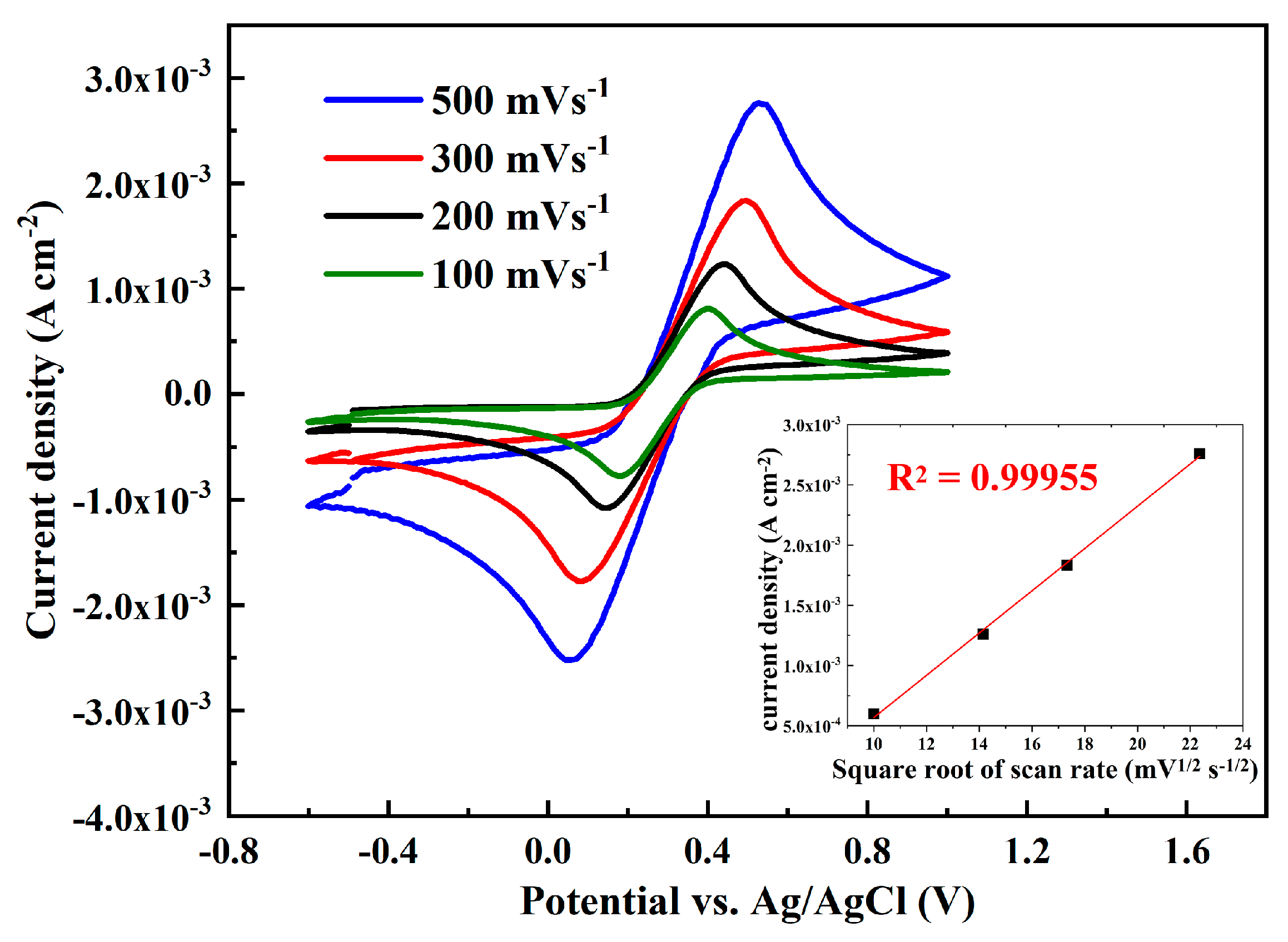
2.2. Electrochemical Characterization

To compare the electrochemical activity of the graphene/ITO electrode with the bare ITO one, CV measurements were recorded in a solution of [Fe(CN)6]3−/4− at a sweep rate of 100 mVs−1 (Figure 3a).
The signal of the bare ITO electrode shows a quasi-reversible redox peak at ≈0.4 V (anodic peak) and a cathodic peak at ≈0.15 V (curve i). Once the ITO surface was modified with graphene, one can clearly see that the anodic and cathodic peaks increased drastically, revealing an enhancement of the electrode electrical conductivity (curve ii). This was confirmed by the EIS technique (Figure 3b). It shows a charge–transfer-limited process and a linear part relative to a diffusion process. The diameter of the semicircle on the Nyquist plots corresponds to the charge–transfer resistance, Rct. The modification of the ITO surface with graphene induces the decrease of the Rct (Figure 3b, curve ii). In fact, it is clear that after the functionalization of the ITO electrode with the graphene layer, the modified ITO electrode impedance plot spectrum shows a smaller semicircle with a smaller diameter. This implies a drastic decrease of about five times in the charge transfer resistance Rct from ~320 Ω (curve i) to ~60 Ω (curve ii), which justifies the enhancement of the electrode electrical conductivity.
At the same conditions, the dependence of the cyclic voltammetric curves on the scan rate was evaluated and presented in Figure 4. The CVs recorded at different sweep rates reveal that anodic currents have a linear dependence on the square root of the sweep rate (ν1/2) in the range between 100 and 500 mV s−1 (inset of Figure 4). Moreover, the peak-to-peak separation has increased, and the peak potential was shifted to more anodic values with the increase in the scan rate, suggesting a diffusion-controlled electrochemical process [55].

2.3. Analytical Performance of the Probe

Recognizing and regulating non-covalent interactions of DNA with solvent and redox-active molecules offers chances to improve the electrochemical signal and can be a useful tool to create a suitable amperometric biosensor. This section describes the modifications of the electrochemical response of one-electron electrochemical transfer reactions of the [Fe(CN)6]3−/4− active-redox probe, induced by the addition of DNA fragments with a known number of base-pairs (bps). In each of these assays, [Fe(CN)6]3−/4− serves primarily as a scaffold to bring DNA into direct contact with the graphene electrode surface. The electrochemical measurements were conducted in full DPV conditions (each experiment was run in triplicate to confirm the reproducibility of the measurements) with a 10 mVs−1 scan rate, 50 mV pulse amplitude, and 50 ms pulse width. The DPV measurements show that the addition of DNA fragments to [Fe(CN)6]3−/4− redox-intermediate buffered solution (E = 221 mV) at a size of 607, 521, 500, and 459 bps provoke cathodic potential shifts of the redox signal, respectively, to 218, 221, 223, and 225 mV (Figure 5a). This variation of the potential is crucial in biosensing since it is characteristic of each DNA size. The observed potential shift can be explained by a harder oxidation of the redox-active intermediate due to steric hindrance to the electron transfer. In fact, double helix DNA oligonucleotides carried negatively charged phosphate groups provoking electrostatic repulsion in the presence of [Fe(CN)6]3−/4− ions. This potential variation is accompanied by a variation of the current explained by a catalytic effect exerted by the DNA molecules. These results are confirmed using EIS in the same conditions (Figure 5b). Nyquist plots obtained by simulation of the impedance spectroscopy data using the Randles circuit (inset of Figure 5b) show that Rct, which describes the charge transfer resistance, decreases gradually with the increase of the number of base pairs of the DNA molecules, while Rs (the resistance of the solution) increases according to the increase of the number of base pairs. In fact, an increase in the DNA base pairs number provided a higher catalytic activity and promoted a faster electron transfer, resulting in a decrease of the semicircles’ diameters and, thus, a decrease in the charge transfer resistance, Rct. The difference in the electrical signal might be due to the kinetic binding of DNA at the electrode surface or in the solution. As a result, a charge transfer resistance is produced, representing the number of bound molecules. The shape of a Nyquist plot is indeed dependent on the electrochemical responses taking place at the surface of the graphene electrode and in the solution. Graphene is very popular for sensor surface modification thanks to its advantages of high electrical conductivity, large surface area, and biocompatibility. DPV measurements recorded at the same conditions on the bare electrode (ITO without graphene) did not show any variation of electrochemical behavior following the addition of DNA (results not shown).
Having a redox signal proportional to the DNA fragment’s size is of crucial importance since this approach will open new perspectives to develop electrochemical-based techniques that could replace nucleic acid gel electrophoresis. Indeed, the latter is the standard technique used in molecular biology to assess both the presence of a DNA fragment and its approximate size by means of a DNA marker. This technique has the disadvantage of being time-consuming as it requires at least one hour between preparing the electrophoresis gel and the migration of the PCR products that should be carefully incorporated into that gel. Other techniques have been developed, but they are not widely used because of the high cost of the machine and the reagents. If the present method is optimized, it can be an alternative to the standard nucleic acid gel electrophoresis system.
Calibration curves for the detection and quantification of the DNA size in terms of the base pairs number are plotted for DPV and Rct, based on DPV and EIS results, in the range 495–607 bps, and are presented in Figure 5c,d. The calibration of DPV intensity and Rct vs. DNA base pairs number were linear in the range of 495–607 bps. The proposed method could be applied as an alternative to the nucleic acid gel electrophoresis technique to verify the presence of a DNA fragment and quantify its size.
The variation of the electrochemical response as a function of the base pair number might be improved. These fluctuations could be induced by differences in the DNA concentration, the GC % of each DNA fragment and, consequently, its 3D structure.

3. Materials and Methods

3.1. Graphene Growth

Copper (Cu) foil substrates with 99.8 wt.% purity and 25 µm thickness from Alfa-Aesar were used for the CVD graphene growth (Electrorava, Turin, Italy). To remove any contamination, the copper foil samples were sonicated, using a DU-32 ultrasonic cleaner from Argolab, in acetone and isopropanol (ACS reagent, purity ≥ 99.5%, Sigma-Aldrich, St. Louis, MO, USA) successively, 10 min each. The substrates were then inserted into the furnace (OTF-1200X, MTI Corporation, Richmond, CA, USA) and heated at 1030 °C under a controlled atmosphere of hydrogen and argon (H2/Ar, Alphagaz, purity > 99.999%) with flow rates of 8 sccm (standard cubic centimeter per min) and 100 sccm, respectively, for 1 h, in order to oxidize the Cu surface for a better quality of the graphene. During graphene growth, the temperature was kept at 1030 °C, and methane (CH4, N55, purity > 99.9995%) was injected (24 sccm) for 30 min.

3.2. Graphene Transfer

Once synthesized, graphene samples were coated with a polymethylmethacrylate (PMMA, Sigma-Aldrich) film of a few micrometers using a spin coater (WS 400BZ 6NPP LITE Rev MS, Laurell, MI, USA). After drying overnight, the samples were then immersed in 1 M ferric chloride solution (FeCl3, purity ≥ 99.99%, Sigma-Aldrich) for 1 h to dissolve the copper foil. To remove any metal residues, the PMMA/graphene films were immersed in a solution of diluted HCl (2%, ACS reagent, 37%, Sigma-Aldrich) for 30 min, then cleaned twice for 10 min each, using DI (deionized) water. The graphene was afterward transferred to SiO2 substrates (Silicon substrates with 100 nm SiO2 layer, Swansea, UK) for Raman spectroscopy measurements and to indium tin oxide substrates (ITO, Neurotech Analytical Instruments, Berlin, CT, USA) for the electrochemical measurements. The PMMA was finally removed using an acetone bath for 1 h. The transferred graphene samples were rinsed using isopropanol, then DI water, and finally dried using nitrogen (N2) flow.

3.3. Graphene Characterization

The surface of graphene/copper foil was analyzed prior to the transfer using the FEI NovaNanoSEM 650 scanning electron microscope (SEM, FEI Co., Hillsboro, OR, USA). Secondary electron scanning mode was used to collect SEM images (5 mm operating distance and 2 kV applied voltage). A Nikon Eclipse L200N optical microscope (Nikon, Minato, Tokyo, Japan) was also used to observe the domain sizes and shapes, as well as the degree of graphene coverage on the copper foil.
A Raman spectrometer, ALPHA300R Confocal RAMAN SYSTEM from WITec GmbH (Ulm, Germany) was used to confirm the quality of the single graphene film. A 532 nm laser excitation was used with a power of 1 mW. A Raman map of the intensities of the graphene G band (IG) and 2D band (I2D) was also performed using the same Raman system.

3.4. Electrochemical Measurements

Aqueous solutions were prepared using deionized water. All reagents and solvents used in the electrochemical measurements were of analytical grade from Sigma-Aldrich and were used without further purification unless otherwise stated. Electrochemical analysis was performed at room temperature employing a three-electrode electrochemical cell comprising ITO substrates as working electrode, an Ag/AgCl 3M (Metrohm, Villebon-sur-Yvette, France) reference electrode, and a platinum wire (Pt, Metrohm, France) as an auxiliary electrode).
The geometric area of the ITO and graphene-coated ITO electrodes was 1 cm2. The immersed part of the ITO electrode was covered with graphene on its whole surface.
The Nova software for electrochemical research (version 1.11) was used to collect data from the PC-controlled Autolab PGSTAT M204 potentiostat equipped with an FRA impedance module (Metrohm, France). All electrochemical measurements were performed in a phosphate-buffered saline solution (PBS) containing 5.0 mM K3Fe(CN)6/K4Fe(CN)6 (at equal proportion) at pH = 7.4.
For the electrochemical impedance spectroscopy (EIS) plots, the ITO and modified ITO electrodes were immersed into a 10 mL phosphate buffer saline (PBS), obtained by dissolving PBS tablets in a required amount of deionized water, containing a mixture of 5 mM concentrations of [Fe(CN)6]4−/3– as a redox probe, and the frequency was swept from 100 kHz to 0.1 Hz at an applied potential of 200 mV with an amplitude modulation of ±20 mV. Nyquist plots are commonly used to represent impedance measurements. In a Nyquist plot, the real part of the impedance is represented in the x-axis, and the imaginary part of the impedance is represented in the y-axis. Each point in the Nyquist plot corresponds to the impedance at one frequency. To fit these plots, the Randles equivalent circuit model (inset of Figure 5b) at a frequency ranging from 100 kHz to 0.1 Hz was used using NOVA (1.11) Metrohm Autolab as simulation software. The fitted circuit is the most used equivalent circuit in electrochemical impedance spectroscopy. It is a model for a semi-infinite diffusion-controlled faradic reaction to the electrode. In this equivalent electrical circuit, all current passes through the solution, which acts as an ohmic resistor, Rs.
Differential pulse voltammetry (DPV) conditions were 10 mVs−1 for the sweep rate, 50 mV for the pulse amplitude, and 50 ms for the pulse width.

3.5. DNA Extraction

Human genomic DNA was extracted from saliva and amplified by Polymerase Chain Reaction (PCR) using specific primers to generate different amplicon sizes (459, 500, 521, and 607 pb). PCR is used in order to amplify a specific segment of DNA. The DNA sample is first heated to a high temperature, typically around 95 °C. This ruptures the hydrogen bonds that hold the two strands of the DNA double helix together, causing the two strands to separate and forming two single-stranded DNA molecules.
The temperature is then reduced to around 50–60 °C, allowing small, complementary DNA sequences known as primers to bind to the single-stranded DNA molecules. Primers are short DNA segments that are designed to match the ends of the target DNA sequence to be amplified.
The temperature is then raised to around 72 °C, which is the optimal temperature for Taq polymerase, a heat-stable enzyme capable of generating new DNA strands. Taq polymerase starts at the primer and adds nucleotides to the 3′ end of the primer to create a new DNA strand. The Taq polymerase then synthesizes a new DNA strand from each of the original single-stranded DNA molecules. The process is repeated many times. Each cycle doubles the amount of DNA in the sample, causing the number of copies of the target DNA sequence to increase rapidly. PCR products were prepared in a sufficient quantity to assess their physicochemical properties.

4. Conclusions

Monolayer graphene was successfully grown and transferred to ITO substrates as an electrode for the electrochemical detection of double-stranded DNA. An enhancement in the electrical conductivity of the graphene-modified ITO electrode was observed in cyclic voltammetry and confirmed by electrochemical impedance spectroscopy. [Fe(CN)6]3−/4− redox couple was used as an electrochemical probe capable of differentiating between double-stranded DNAs at different sizes (depending on the number of base pairs). A potential variation was observed and accompanied by a current variation due to a catalytic effect exerted by the DNA molecules on the ferri/ferrocyanide redox probe. These behaviors were confirmed by the EIS characterization, where a decrease of the charge transfer resistance Rct is observed with the increase of the DNA base pairs number. Calibration curves of current density and Rct showed linear variations. These results open interesting perspectives to understanding DNA double helix behavior involving amperometric and potentiometric double-stranded DNA biosensors as potential alternatives to classical molecular biology techniques commonly used to differentiate DNA fragments based on their size. If optimized, the current approach may replace the conventional nucleic acid gel electrophoresis system.

Author Contributions

Conceptualization A.B., A.H. and O.M.; methodology, A.H., A.B., R.E., R.O., M.A.A. and O.M.; investigation, A.H., R.E., R.O. and M.A.A.; writing—original draft preparation, A.B. and A.H.; writing—review and editing, D.M.F.S. and O.M.; visualization, D.M.F.S.; resources, R.C.; supervision, R.C. All authors have read and agreed to the published version of the manuscript.

Funding

This study was funded by the Arab-German Young Academy of Sciences and Humanities (AGYA). AGYA draws on the financial support of the German Federal Ministry of Education and Research (BMBF (grant number 01DL20003). Fundação para a Ciência e a Tecnologia (FCT, Portugal) is acknowledged for a research contract in the scope of programmatic funding UIDP/04540/2020 (D.M.F. Santos).

Data Availability Statement

The authors confirm that all relevant data generated during this study are included in this published article.

Acknowledgments

This work was supported by the Arab-German Young Academy of Sciences and Humanities (AGYA) and within its interdisciplinary setting.

Conflicts of Interest

The authors declare no conflict of interest. The funders have no role in the design of the study; in the collection, analyses, or interpretation of data; in the writing of the manuscript; or in the decision to publish the results.

References

  1. Yu, F.; Camilli, L.; Wang, T.; Mackenzie, D.M.A.; Curioni, M.; Akid, R.; Bøggild, P. Complete long-term corrosion protection with chemical vapor deposited graphene. Carbon 2018, 132, 78–84. [Google Scholar] [CrossRef]
  2. Stöberl, U.; Wurstbauer, U.; Wegscheider, W.; Weiss, D.; Eroms, J. Morphology and flexibility of graphene and few-layer graphene on various substrates. Appl. Phys. Lett. 2008, 93, 51906. [Google Scholar] [CrossRef]
  3. Novoselov, K.S.; Morozov, S.V.; Mohinddin, T.M.G.; Ponomarenko, L.A.; Elias, D.C.; Yang, R.; Barbolina, I.I.; Blake, P.; Booth, T.J.; Jiang, D.; et al. Electronic properties of graphene. Phys. Status Solidi 2007, 244, 4106–4111. [Google Scholar] [CrossRef]
  4. Li, X.; Tao, L.; Chen, Z.; Fang, H.; Li, X.; Wang, X.; Xu, J.-B.; Zhu, H. Graphene and related two-dimensional materials: Structure-property relationships for electronics and optoelectronics. Appl. Phys. Rev. 2017, 4, 21306. [Google Scholar] [CrossRef]
  5. Novoselov, K.S. Electric Field Effect in Atomically Thin Carbon Films. Science 2004, 306, 666–669. [Google Scholar] [CrossRef]
  6. El-Kady, M.F.; Strong, V.; Dubin, S.; Kaner, R.B. Laser Scribing of High-Performance and Flexible Graphene-Based Electrochemical Capacitors. Science 2012, 335, 1326–1330. [Google Scholar] [CrossRef]
  7. Gao, H.; Yang, H.; Wang, S.; Li, D.; Wang, F.; Fang, L.; Lei, L.; Xiao, Y.; Yang, G. A new route for the preparation of CoAl2O4 nanoblue pigments with high uniformity and its optical properties. J. Sol-Gel Sci. Technol. 2018, 86, 206–216. [Google Scholar] [CrossRef]
  8. Scidà, A.; Haque, S.; Treossi, E.; Robinson, A.; Smerzi, S.; Ravesi, S.; Borini, S.; Palermo, V. Application of graphene-based flexible antennas in consumer electronic devices. Mater. Today 2018, 21, 223–230. [Google Scholar] [CrossRef]
  9. Qu, Y.; He, F.; Yu, C.; Liang, X.; Liang, D.; Ma, L.; Zhang, Q.; Lv, J.; Wu, J. Advances on graphene-based nanomaterials for biomedical applications. Mater. Sci. Eng. C 2018, 90, 764–780. [Google Scholar] [CrossRef]
  10. Karyaoui, M.; Jemia, D.B.; Daoudi, M.; Bardaoui, A.; Boukhachem, A.; Amlouk, M.; Chtourou, R. Physical properties of graphene oxide GO-doped ZnO thin films for optoelectronic application. Appl. Phys. A 2021, 127, 134. [Google Scholar] [CrossRef]
  11. Jemia, D.B.; Karyaoui, M.; Wederni, M.A.; Bardaoui, A.; Martinez-Huerta, M.V.; Amlouk, M.; Chtourou, R. Photoelectrochemical activity of ZnO:Ag/rGO photo-anodes synthesized by two-steps sol-gel method. Chin. Phys. B 2022, 31, 58201. [Google Scholar] [CrossRef]
  12. Li, J.; Liu, J.; Liu, J.; Lai, J.; Chen, Y.; Li, W. Graphene-Based Composite Membrane Prepared from Solid Carbon Source Catalyzed by Ni Nanoparticles. Nanomaterials 2021, 11, 3392. [Google Scholar] [CrossRef] [PubMed]
  13. Choi, H.Y.; Shin, E.J.; Lee, S.H. Design and evaluation of 3D-printed auxetic structures coated by CWPU/graphene as strain sensor. Sci. Rep. 2022, 12, 7780. [Google Scholar] [CrossRef]
  14. Zhang, H.; He, R.; Niu, Y.; Han, F.; Li, J.; Zhang, X.; Xu, F. Graphene-enabled wearable sensors for healthcare monitoring. Biosens. Bioelectron. 2022, 197, 113777. [Google Scholar] [CrossRef] [PubMed]
  15. Fu, L.; Mao, S.; Chen, F.; Zhao, S.; Su, W.; Lai, G.; Yu, A.; Lin, C.-T. Graphene-based electrochemical sensors for antibiotic detection in water, food and soil: A scientometric analysis in CiteSpace (2011–2021). Chemosphere 2022, 297, 134127. [Google Scholar] [CrossRef]
  16. Kwon, B.; Bae, H.; Lee, H.; Kim, S.; Hwang, J.; Lim, H.; Lee, J.H.; Cho, K.; Ye, J.; Lee, S.; et al. Ultrasensitive N-Channel Graphene Gas Sensors by Nondestructive Molecular Doping. ACS Nano 2022, 16, 2176–2187. [Google Scholar] [CrossRef] [PubMed]
  17. Whitener, K.E.; Sheehan, P.E. Graphene synthesis. Diam. Relat. Mater. 2014, 46, 25–34. [Google Scholar] [CrossRef]
  18. Yu, H.; Zhang, B.; Bulin, C.; Li, R.; Xing, R. High-efficient Synthesis of Graphene Oxide Based on Improved Hummers Method. Sci. Rep. 2016, 6, 36143. [Google Scholar] [CrossRef]
  19. Li, X.; Cai, W.; An, J.; Kim, S.; Nah, J.; Yang, D.; Piner, R.; Velamakanni, A.; Jung, I.; Tutuc, E.; et al. Large-Area Synthesis of High-Quality and Uniform Graphene Films on Copper Foils. Science 2009, 324, 1312. [Google Scholar] [CrossRef] [PubMed]
  20. Deng, B.; Liu, Z.; Peng, H. Toward Mass Production of CVD Graphene Films. Adv. Mater. 2019, 31, 1800996. [Google Scholar] [CrossRef]
  21. Qing, F.; Hou, Y.; Stehle, R.; Li, X. Chemical vapor deposition synthesis of graphene films. APL Mater. 2019, 7, 20903. [Google Scholar] [CrossRef]
  22. Losurdo, M.; Giangregorio, M.M.; Capezzuto, P.; Bruno, G. Graphene CVD growth on copper and nickel: Role of hydrogen in kinetics and structure. Phys. Chem. Chem. Phys. 2011, 13, 20836. [Google Scholar] [CrossRef] [PubMed]
  23. Moon, J.-M.; Thapliyal, N.; Hussain, K.K.; Goyal, R.N.; Shim, Y.-B. Conducting polymer-based electrochemical biosensors for neurotransmitters: A review. Biosens. Bioelectron. 2018, 102, 540–552. [Google Scholar] [CrossRef] [PubMed]
  24. Asal, M.; Özen, Ö.; Şahinler, M.; Polatoğlu, İ. Recent Developments in Enzyme, DNA and Immuno-Based Biosensors. Sensors 2018, 18, 1924. [Google Scholar] [CrossRef] [PubMed]
  25. Verma, M.L.; Sukriti; Dhanya, B.S.; Saini, R.; Das, A.; Varma, R.S. Synthesis and application of graphene-based sensors in biology: A review. Environ. Chem. Lett. 2022, 20, 2189–2212. [Google Scholar] [CrossRef]
  26. Kim, H.E.; Schuck, A.; Lee, J.H.; Kim, Y.-S. Solution-gated graphene field effect transistor for TP53 DNA sensor with coplanar electrode array. Sens. Actuators B Chem. 2019, 291, 96–101. [Google Scholar] [CrossRef]
  27. Xia, Y.; Sun, Y.; Li, H.; Chen, S.; Zhu, T.; Wang, G.; Man, B.; Pan, J.; Yang, C. Plasma treated graphene FET sensor for the DNA hybridization detection. Talanta 2021, 223, 121766. [Google Scholar] [CrossRef]
  28. Zheng, C.; Huang, L.; Zhang, H.; Sun, Z.; Zhang, Z.; Zhang, G.-J. Fabrication of Ultrasensitive Field-Effect Transistor DNA Biosensors by a Directional Transfer Technique Based on CVD-Grown Graphene. ACS Appl. Mater. Interfaces 2015, 7, 16953–16959. [Google Scholar] [CrossRef]
  29. Huang, J.; Liu, Y.; You, T. Carbon nanofiber based electrochemical biosensors: A review. Anal. Methods 2010, 2, 202. [Google Scholar] [CrossRef]
  30. Wang, Y.-H.; Huang, K.-J.; Wu, X. Recent advances in transition-metal dichalcogenides based electrochemical biosensors: A review. Biosens. Bioelectron. 2017, 97, 305–316. [Google Scholar] [CrossRef]
  31. Xu, Y.; Cheng, G.; He, P.; Fang, Y. A Review: Electrochemical Aptasensors with Various Detection Strategies. Electroanalysis 2009, 21, 1251–1259. [Google Scholar] [CrossRef]
  32. Campuzano, S.; Pedrero, M.; García, J.L.; García, E.; García, P.; Pingarrón, J.M. Development of amperometric magnetogenosensors coupled to asymmetric PCR for the specific detection of Streptococcus pneumoniae. Anal. Bioanal. Chem. 2011, 399, 2413–2420. [Google Scholar] [CrossRef] [PubMed]
  33. Sotillo, A.; Pedrero, M.; de Pablos, M.; García, J.L.; García, E.; García, P.; Pingarrón, J.M.; Mingorance, J.; Campuzano, S. Clinical evaluation of a disposable amperometric magneto-genosensor for the detection and identification of Streptococcus pneumoniae. J. Microbiol. Methods 2014, 103, 25–28. [Google Scholar] [CrossRef] [PubMed]
  34. Wang, C.-F.; Sun, X.-Y.; Su, M.; Wang, Y.-P.; Lv, Y.-K. Electrochemical biosensors based on antibody, nucleic acid and enzyme functionalized graphene for the detection of disease-related biomolecules. Analyst 2020, 145, 1550–1562. [Google Scholar] [CrossRef]
  35. Xu, B.; Hu, Y.; Shu, Q.; Wang, M.; Chen, Z.; Wei, W.; Wen, J.; Li, R.; Liao, F.; Cheng, L.; et al. A sensitive electrochemical DNA sensor based on reduced graphene oxide modified electrode. J. Chin. Chem. Soc. 2022, 69, 822–830. [Google Scholar] [CrossRef]
  36. Bo, Y.; Yang, H.; Hu, Y.; Yao, T.; Huang, S. A novel electrochemical DNA biosensor based on graphene and polyaniline nanowires. Electrochim. Acta 2011, 56, 2676–2681. [Google Scholar] [CrossRef]
  37. Peña-Bahamonde, J.; Nguyen, H.N.; Fanourakis, S.K.; Rodrigues, D.F. Recent advances in graphene-based biosensor technology with applications in life sciences. J. Nanobiotechnol. 2018, 16, 75. [Google Scholar] [CrossRef]
  38. Hammami, A.; Raouafi, N.; Mirsky, V.M. Electrically controlled Michael addition: Addressing of covalent immobilization of biological receptors. Biosens. Bioelectron. 2018, 121, 72–79. [Google Scholar] [CrossRef]
  39. Alhazmi, H.A.; Ahsan, W.; Mangla, B.; Javed, S.; Hassan, M.Z.; Asmari, M.; Bratty, M.A.; Najmi, A. Graphene-based biosensors for disease theranostics: Development, applications, and recent advancements. Nanotechnol. Rev. 2022, 11, 96–116. [Google Scholar] [CrossRef]
  40. Furst, A.L.; Hill, M.G.; Barton, J.K. Electrocatalysis in DNA sensors. Polyhedron 2014, 84, 150–159. [Google Scholar] [CrossRef]
  41. Hong, G.; Chen, R.; Xu, L.; Lu, X.; Yang, Z.; Zhou, G.; Li, L.; Chen, W.; Peng, H. One-pot ultrasonic synthesis of multifunctional Au nanoparticle-ferrocene-WS2 nanosheet composite for the construction of an electrochemical biosensing platform. Anal. Chim. Acta 2020, 1099, 52–59. [Google Scholar] [CrossRef] [PubMed]
  42. Kim, E.; Kim, K.; Yang, H.; Kim, Y.T.; Kwak, J. Enzyme-Amplified Electrochemical Detection of DNA Using Electrocatalysis of Ferrocenyl-Tethered Dendrimer. Anal. Chem. 2003, 75, 5665–5672. [Google Scholar] [CrossRef] [PubMed]
  43. Lapierre-Devlin, M.A.; Asher, C.L.; Taft, B.J.; Gasparac, R.; Roberts, M.A.; Kelley, S.O. Amplified Electrocatalysis at DNA-Modified Nanowires. Nano Lett. 2005, 5, 1051–1055. [Google Scholar] [CrossRef]
  44. Yang, H.; Hui, A.; Pampalakis, G.; Soleymani, L.; Liu, F.-F.; Sargent, E.H.; Kelley, S.O. Direct, Electronic MicroRNA Detection for the Rapid Determination of Differential Expression Profiles. Angew. Chem. Int. Ed. 2009, 48, 8461–8464. [Google Scholar] [CrossRef]
  45. Jayakumar, K.; Rajesh, R.; Dharuman, V.; Venkatasan, R.; Hahn, J.H.; Karutha Pandian, S. Gold nano particle decorated graphene core first generation PAMAM dendrimer for label free electrochemical DNA hybridization sensing. Biosens. Bioelectron. 2012, 31, 406–412. [Google Scholar] [CrossRef]
  46. Lim, C.X.; Hoh, H.Y.; Ang, P.K.; Loh, K.P. Direct Voltammetric Detection of DNA and pH Sensing on Epitaxial Graphene: An Insight into the Role of Oxygenated Defects. Anal. Chem. 2010, 82, 7387–7393. [Google Scholar] [CrossRef]
  47. Dubuisson, E.; Yang, Z.; Loh, K.P. Optimizing Label-Free DNA Electrical Detection on Graphene Platform. Anal. Chem. 2011, 83, 2452–2460. [Google Scholar] [CrossRef]
  48. Benvidi, A.; Tezerjani, M.D.; Jahanbani, S.; Mazloum Ardakani, M.; Moshtaghioun, S.M. Comparison of impedimetric detection of DNA hybridization on the various biosensors based on modified glassy carbon electrodes with PANHS and nanomaterials of RGO and MWCNTs. Talanta 2016, 147, 621–627. [Google Scholar] [CrossRef] [PubMed]
  49. Benvidi, A.; Saucedo, N.M.; Ramnani, P.; Villarreal, C.; Mulchandani, A.; Tezerjani, M.D.; Jahanbani, S. Electro-oxidized Monolayer CVD Graphene Film Transducer for Ultrasensitive Impedimetric DNA Biosensor. Electroanalysis 2018, 30, 1791–1800. [Google Scholar] [CrossRef]
  50. Chen, S.; Brown, L.; Levendorf, M.; Cai, W.; Ju, S.-Y.; Edgeworth, J.; Li, X.; Magnuson, C.W.; Velamakanni, A.; Piner, R.D.; et al. Oxidation Resistance of Graphene-Coated Cu and Cu/Ni Alloy. ACS Nano 2011, 5, 1321–1327. [Google Scholar] [CrossRef]
  51. Jia, C.; Jiang, J.; Gan, L.; Guo, X. Direct Optical Characterization of Graphene Growth and Domains on Growth Substrates. Sci. Rep. 2012, 2, 707. [Google Scholar] [CrossRef] [PubMed]
  52. Nemanich, R.J.; Lucovsky, G.; Solin, S.A. Infrared active optical vibrations of graphite. Solid State Commun. 1977, 23, 117–120. [Google Scholar] [CrossRef]
  53. Piscanec, S.; Lazzeri, M.; Mauri, F.; Ferrari, A.C.; Robertson, J. Kohn Anomalies and Electron-Phonon Interactions in Graphite. Phys. Rev. Lett. 2004, 93, 185503. [Google Scholar] [CrossRef] [PubMed]
  54. Ferrari, A.C.; Basko, D.M. Raman spectroscopy as a versatile tool for studying the properties of graphene. Nat. Nanotechnol. 2013, 8, 235–246. [Google Scholar] [CrossRef]
  55. Hammami, A.; Rabti, A.; Raouafi, N. A novel electrochemical and chromogenic guest-responsive anisidine-based chemosensor for transition metallic cations. J. Electroanal. Chem. 2014, 731, 179–183. [Google Scholar] [CrossRef]
Figure 1. (a) Optical micrograph of the surface of the graphene/copper foil, under 20-times magnification; (b) SEM image of graphene/copper foil.
Inorganics 11 00173 g001
Figure 2. (a) Raman spectra of monolayer graphene transferred on SiO2/Si substrate; (b) 2D to G peak intensities ratio (I2D/IG) mapping.
Inorganics 11 00173 g002
Figure 3. (a) Cyclic voltammetry at a sweep rate of 100 mVs−1 and (b) EIS spectra of the bare ITO electrode (i) and of the same electrode after graphene transfer (ii); all experiments are recorded in 0.1 M KCl solution containing 5 mM K3[Fe(CN)6]/K4[Fe(CN)6].
Inorganics 11 00173 g003
Figure 4. Cyclic voltammetry of the graphene-modified electrode as a function of the scan rate. Inset: anodic currents linear dependence on the square root of the sweep rate (ν1/2). All experiments are recorded in 0.1 M KCl solution containing 5 mM K3[Fe(CN)6]/K4[Fe(CN)6].
Inorganics 11 00173 g004
Figure 5. Electrochemical responses of [Fe(CN)6]3−/4− probe capturing at different bps nucleotides in 0.1 M KCl phosphate buffer solution (pH = 7.4) using (a) DPV and (b) EIS spectra presented as Nyquist plots in the frequency range from 0.1 Hz to 100 kHz at +0.2 V. The inset is the Randles equivalent circuit model used for EIS analysis, where Rs is the electrolyte resistance, Rct is the charge transfer resistance, CPE is the constant phase element, and ZW is the Warburg diffusion element. (c) Calibration of current density, potential, and (d) Rct vs. DNA base pairs number.
Inorganics 11 00173 g005
Disclaimer/Publisher’s Note: The statements, opinions and data contained in all publications are solely those of the individual author(s) and contributor(s) and not of MDPI and/or the editor(s). MDPI and/or the editor(s) disclaim responsibility for any injury to people or property resulting from any ideas, methods, instructions or products referred to in the content.

