1. Introduction
Semiconducting metal chalcogenides have reached notable achievements as absorbers in photovoltaic modules [
1]. As the representative, cadmium telluride (CdTe) solar cells have overcome the power conversion efficiency (PCE) of 22% [
1]. However, Te reserves are rather low on Earth, and Cd is highly toxic, which seriously restricts its application [
2,
3,
4]. Therefore, it is necessary to develop earth-abundant and non-toxic materials as alternative light absorbers. Among various metal chalcogenides, Sb
2(S, Se)
3 has attracted more and more attention in recent years because of its optimal bandgap (1.1~1.7 eV), high absorption coefficient (>10
5 cm), and excellent stability [
3,
4,
5]. So far, great progress has been made on Sb
2(S, Se)
3 solar cells [
2,
4,
5,
6,
7]. Chen et al. have successfully developed a one-step hydrothermal method to grow high-quality Sb
2(S, Se)
3 film with the device structure of FTO/CdS/Sb
2(S, Se)
3/Spiro-OMeTAD/Au, which promoted the PCE to over 10% [
4].
However, the best-performed devices required Spiro-OMeTAD as the hole transport material (HTM), which has several drawbacks in terms of commercialization [
4,
6]. The synthesis of Spiro-OMeTAD involves several complex reactions, which require harsh conditions (−78 °C) and aggressive reagents (Br
2) [
8,
9]. Its total yield is less than 30% when synthesized from commercially available raw materials. In addition, highly pure sublimation-grade Spiro-OMeTAD is required to fabricate high-performance solar cells. The result is that its price has surpassed USD 100 per gram, which is too expensive for large-scale usage [
6]. Furthermore, Spiro-OMeTAD needs hygroscopic dopants to improve its conductivity, which accelerates the degradation of solar cells [
10,
11]. Similarly, a dithieno [3,2-b:2′,3′-d] pyrrole-cored small molecule (DTPThMe-ThTPA) has proved to be another efficient HTM. However, it also needs Li-TFSI dopants and the cost for the synthesis of DTPThMe-ThTPA is still relatively high, around USD 20 per gram [
6]. The HTM-free Sb
2(S, Se)
3 solar cells showed much better stability than the ones employing doped Spiro-OMeTAD [
4]. For the counter electrode materials, precious metals, such as gold, were commonly used for Sb
2(S, Se)
3 solar cells. These need to be deposited in a vacuum, which further pushed up the fabrication costs [
3,
4,
6]. These unsolved problems of low stability and high cost seriously hamper the industrial application of Sb
2(S, Se)
3 in photovoltaics. In this regard, stable and low-cost HTMs and electrode materials are in strong demand.
Poly(3-hexylthiophene) (P3HT) is an alternative polymer HTM with outstanding optoelectronic properties [
12,
13]. It needs 3 steps to be synthesized with over 60% total yield, which means its cost-per-gram is relatively low among various organic HTMs [
13,
14]. Aside from these, it could be directly used in solar cells without dopants, which benefits its stability [
10]. For the counter electrode materials, carbon materials have a work function of ~5 eV, which is close to the work function of Au (~4.6 eV) [
15,
16,
17]. Furthermore, they have remarkable advantages in abundance, price competence, and stability, which make them an excellent option as a counter electrode for solar cells [
15]. In this way, developing Sb
2(S, Se)
3 solar cells with the discussed materials should be highly promising to reduce fabrication costs.
Herein, Sb2(S, Se)3 solar cells were fabricated with carbon materials as counter electrodes and P3HT as HTM. Since both P3HT and carbon electrodes commonly show poorer hole selectivity, a two-step hydrothermal method was developed to grow high-quality Sb2(S, Se)3 films with a composition and energy level gradient, which would help to enhance hole extraction and charge separation. In detail, Sb2S3 and Sb2(S, Se)3 films were subsequently deposited on a substrate by hydrothermal methods. Then, we employed carbon materials as the counter electrodes and named Sb2(S, Se)3 solar cells without HTMs and precious metal electrodes as carbon-based Sb2(S, Se)3 solar cells. The carbon-based Sb2(S, Se)3 solar cells could achieve a PCE of 2.76%. Furthermore, by inserting a P3HT layer between the Sb2(S, Se)3 film and carbon electrode, hole extraction was significantly enhanced and the PCE was improved to 4.15%.
2. Results and Discussion
As stated above, constructing a suitable energy level gradient via forming a composition gradient could favor hole extraction. However, it is hard to grow a Sb
2(S, Se)
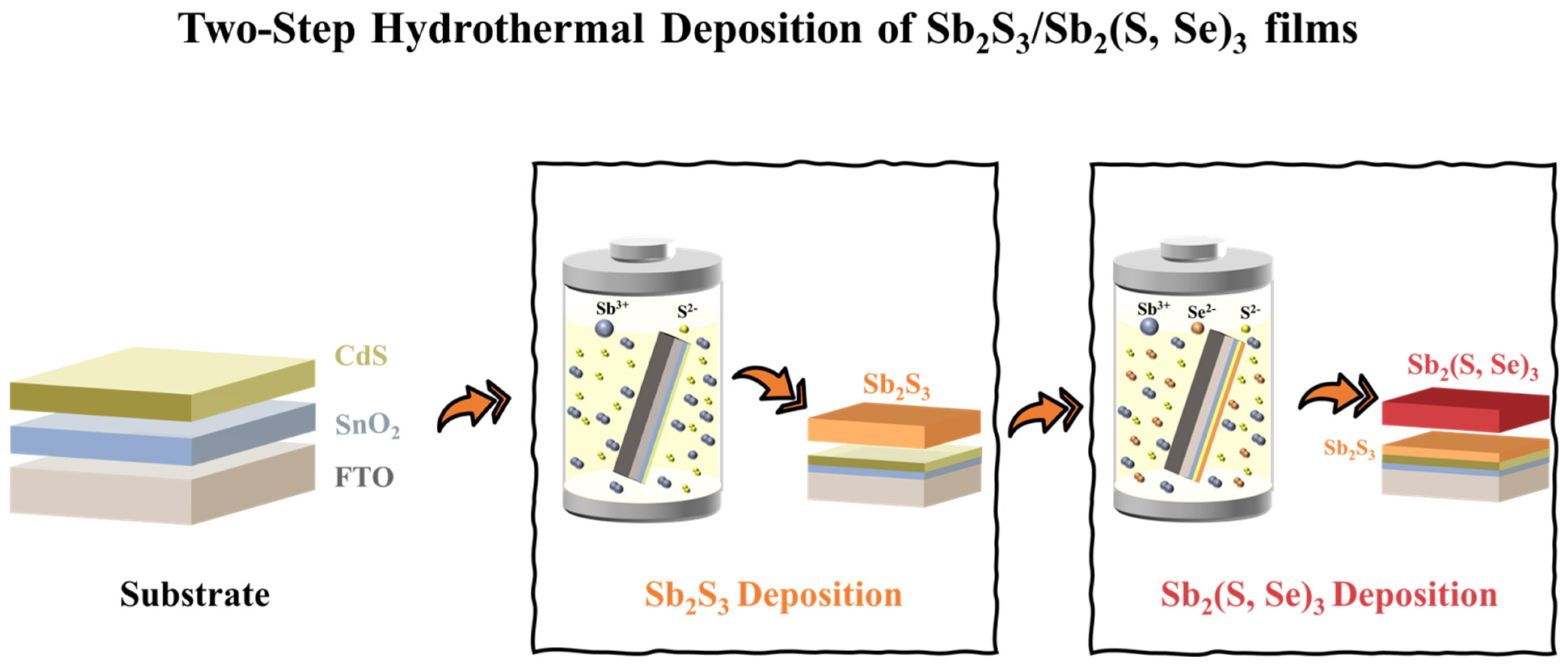
3 layer with a composition gradient by the conventional one-step hydrothermal method. Therefore, in our present work, a two-step hydrothermal method was developed to control the composition gradient. The whole procedure was illustrated in
Figure 1. A Sb
2S
3 layer was firstly grown on the pre-deposited FTO/SnO
2/CdS substrate by the hydrothermal method in the solution containing KSbC
4H
4O
7·0.5H
2O and Na
2S
2O
3·5H
2O. In the second step, selenourea was added to the solution as a Se source for the deposition of the Sb
2(S, Se)
3 layer, and the deposited Sb
2S
3 layer was used as substrate. Finally, the stacked films were annealed at 350 °C for 15 min in a glove box filled with N
2 to get the final targeted films.
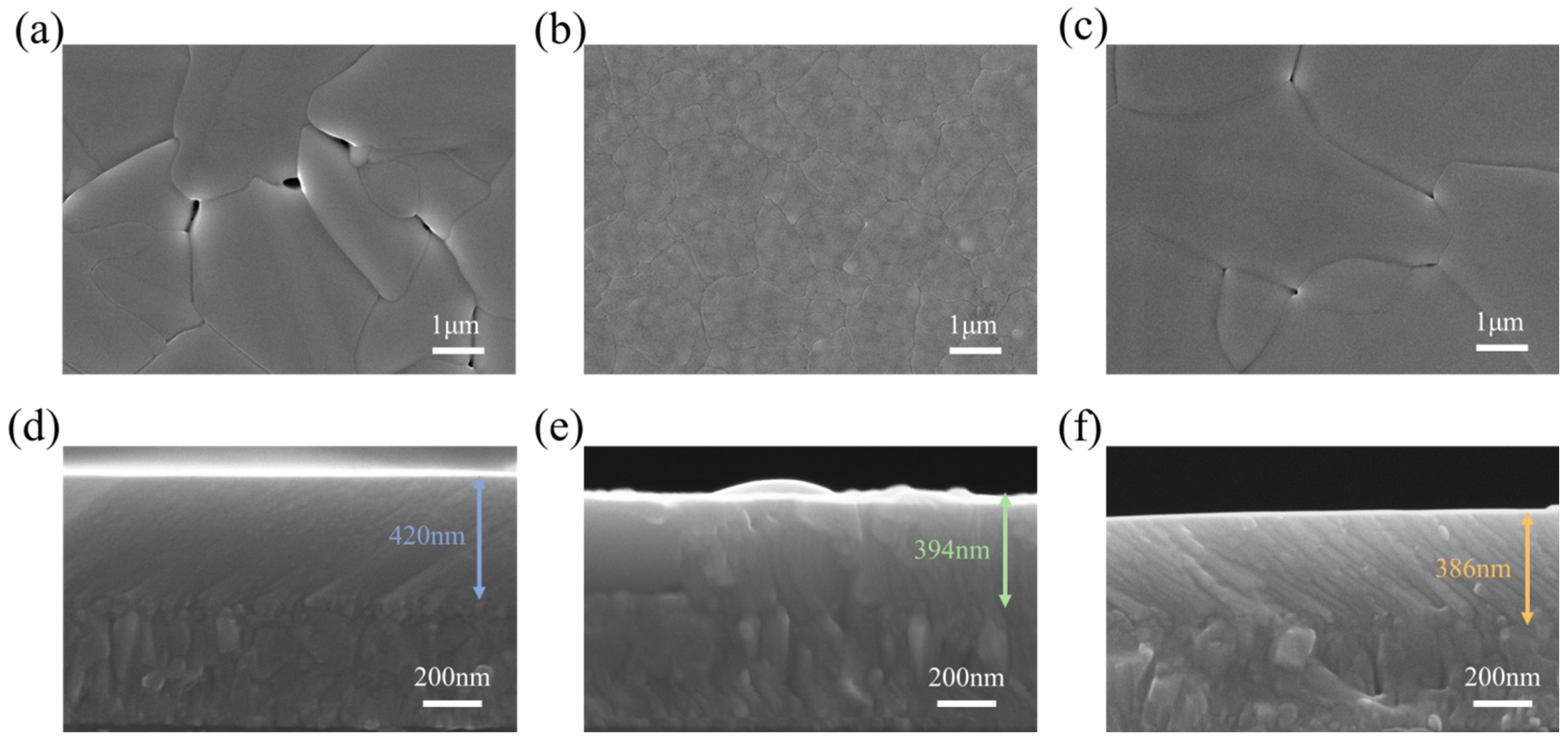
Scanning electron microscopy (SEM) images were taken to characterize the change in the morphology of different films. As shown in
Figure 2a, the Sb
2S
3 film exhibited a flat surface with a large grain size (2~3.5 μm), while many pinholes could also be observed. After the introduction of Se (
Figure 2b), the Sb
2(S, Se)
3 film displayed a much smaller grain size (about 0.5~2 μm) than that of the Sb
2S
3 film and showed no pinholes. Furthermore, the surface of the Sb
2(S, Se)
3 film was significantly rougher than that of the Sb
2S
3 (
Figure 2d,e) film. Surprisingly, when Sb
2S
3 film was used as the substrate for the growth of the Sb
2(S, Se)
3 film, the Sb
2S
3/Sb
2(S, Se)
3 film exhibited a flat surface, large grains, and small pinholes, which combined the advantages of Sb
2S
3 films and Sb
2(S, Se)
3 films (
Figure 2c). Different from the surface morphology, the thicknesses of the three films were similar, around 400 nm (
Figure 2d–f), indicating that the nucleation rate of Sb
2S
3 on CdS film was smaller than that of Sb
2(S, Se)
3 [
17,
18]. In addition, the nucleation rate of Sb
2(S, Se)
3 on CdS film was larger than that on Sb
2S
3 film. As
Figure S1 shows, the hydrothermal reaction time of Sb
2S
3 remarkably affected the morphology of Sb
2S
3/Sb
2(S, Se)
3 films. As the reaction time increased, the grains of Sb
2S
3/Sb
2(S, Se)
3 films enlarged from ~3 μm to tens of micrometers, which indicates that the morphology of Sb
2S
3 films also affects the nucleation rate of Sb
2(S, Se)
3. It has been reported that morphological ordering of compact and large grain size is an important factor in enhancing the performance of thin film solar cells [
19]. Although the longer growth time of Sb
2S
3 films enabled larger grains of stacked films, cracks began to appear on the surface of Sb
2S
3/Sb
2(S, Se)
3 films grown on Sb
2S
3 substrate with a reaction time of 4 h (
Figure S1d). The crack is a kind of defect in semiconductors, which should be avoided to reach high-performance solar cells [
14].
X-ray diffraction (XRD) patterns were recorded to characterize the crystal structures of different films. As depicted in
Figure 3a, almost all the major diffraction peaks of the Sb
2S
3 film could be indexed to the characteristic peaks of standard Sb
2S
3, indicating its existence in all kinds of films [
20]. After selenourea was introduced to precursors, XRD patterns correspondingly shifted toward a low diffraction angle for the Sb
2(S, Se)
3 film, which is due to the incorporation of the large Se
2− ion (
Figure 3b,c). For the Sb
2S
3/Sb
2(S, Se)
3 film, the deposition of the Sb
2(S, Se)
3 film on the Sb
2S
3 film also slightly shifted the XRD peak positions toward lower diffraction angles, indicating the successful incorporation of Se
2− ions (also see
Figure S2). The energy dispersive spectroscopy (EDS) results (
Figure S3) showed that the Se/(S + Se) in the Sb
2S
3, Sb
2(S, Se)
3 and Sb
2S
3/Sb
2(S, Se)
3 films were 0, 23.70% and 20.81%, respectively, which was consistent with the XRD results. As shown in
Figure 3e, the texture coefficient of (221) peaks (TC
(221))/TC
(120) ratio of Sb
2S
3, Sb
2(S, Se)
3 and Sb
2S
3/Sb
2(S, Se)
3 films were calculated to be 0.75, 1.15 and 1.22, respectively. As reported in the literature, Se introduction could increase the TC
(221)/TC
(120) ratio, which indicates that (Sb
4Se
6)
n ribbons grow more perpendicular to the substrate [
3]. A larger TC
(221)/TC
(120) ratio yields small series resistance and thus higher PCE. Therefore, the crystal orientation in the Sb
2S
3/Sb
2(S, Se)
3 film is the most promising one among the three films.
Ultraviolet–visible (UV-vis) spectra were examined to explore the light absorption property of different films. According to the Tauc plots (
Figure 3f), the bandgap (
Eg) of the Sb
2S
3 film is calculated to be 1.72 eV. After the introduction of Se, the
Eg of the Sb
2(S, Se)
3 film is reduced to about 1.58 eV. For the Sb
2S
3/Sb
2(S, Se)
3 films, the
Eg is calculated to be about 1.62 eV, which is between the
Eg of Sb
2(S, Se)
3 film and the
Eg of Sb
2S
3 film.
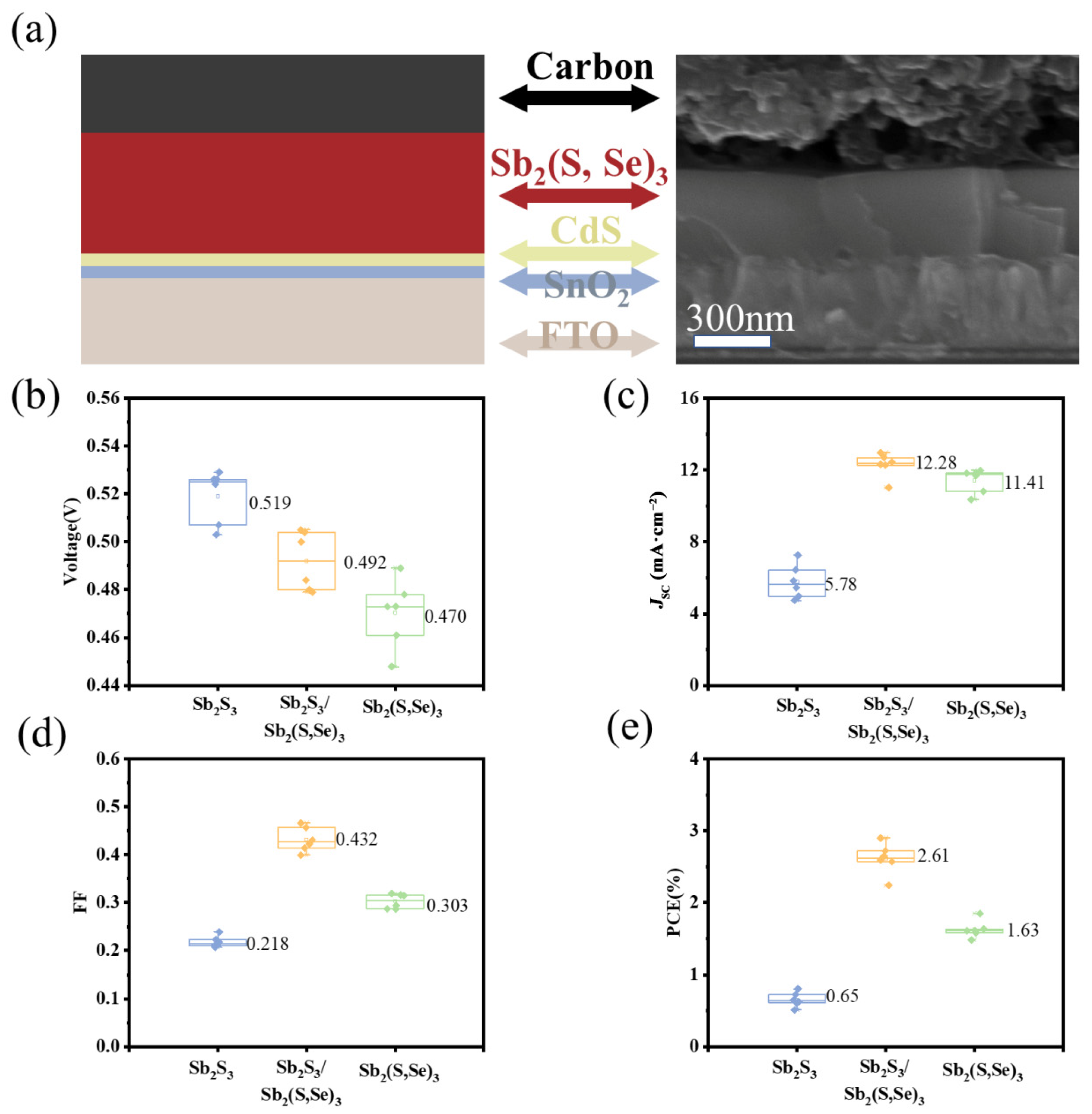
Carbon electrodes with a thickness of tens of micrometers were directly deposited by painting a commercial carbon paste on the Sb
2(S, Se)
3 films followed by annealing treatment at 120 °C for 30 min.
Figure 4a shows the scheme of carbon-based Sb
2(S, Se)
3 solar cells with the structure of FTO/SnO
2/CdS/Sb
2(S, Se)
3/Carbon. A corresponding cross-sectional SEM image of the carbon-based Sb
2(S, Se)
3 solar cells indicates that their interfaces are in intimate contact. Current density–voltage (
J–V) curves under standard AM 1.5G illumination with the light intensity of 100 mW/cm
2 were measured and the statistical data of photovoltaic parameters were shown in
Figure 4b–e. The Sb
2S
3 solar cells displayed a low average PCE (0.65%), with an average open circuit voltage (
VOC) of 0.519 V, short circuit current density (
JSC) of 5.78 mA·cm
−2, and fill factor (FF) of 0.218. For the Sb
2(S, Se)
3 solar cells, the average PCE increased to 1.63%. Though the smaller
Eg would lead to a lower
VOC (0.470 V) than the
VOC of Sb
2S
3 solar cells, the enhancement in light utilization promoted the
JSC to 11.41 mA·cm
−2, which mainly contributed to the improvement of PCE [
21,
22]. The Sb
2S
3/Sb
2(S, Se)
3 solar cells exhibited the highest average PCE of 2.61% among 3 kinds of materials, with a
VOC of 0.492 V,
JSC of 12.28 mA·cm
−2 and FF of 0.432. The improved PCE is mainly benefited from the enhanced FF, which is significantly influenced by the charge extraction of solar cells. The gradient structure of Sb
2S
3/Sb
2(S, Se)
3 yields a gradient band alignment, which is believed to accelerate the charge extraction within it [
14,
20,
23,
24].
To further reinforce hole extraction, the stable and cost-effective HTM, P3HT, was employed as an interlayer between the Sb
2S
3/Sb
2(S, Se)
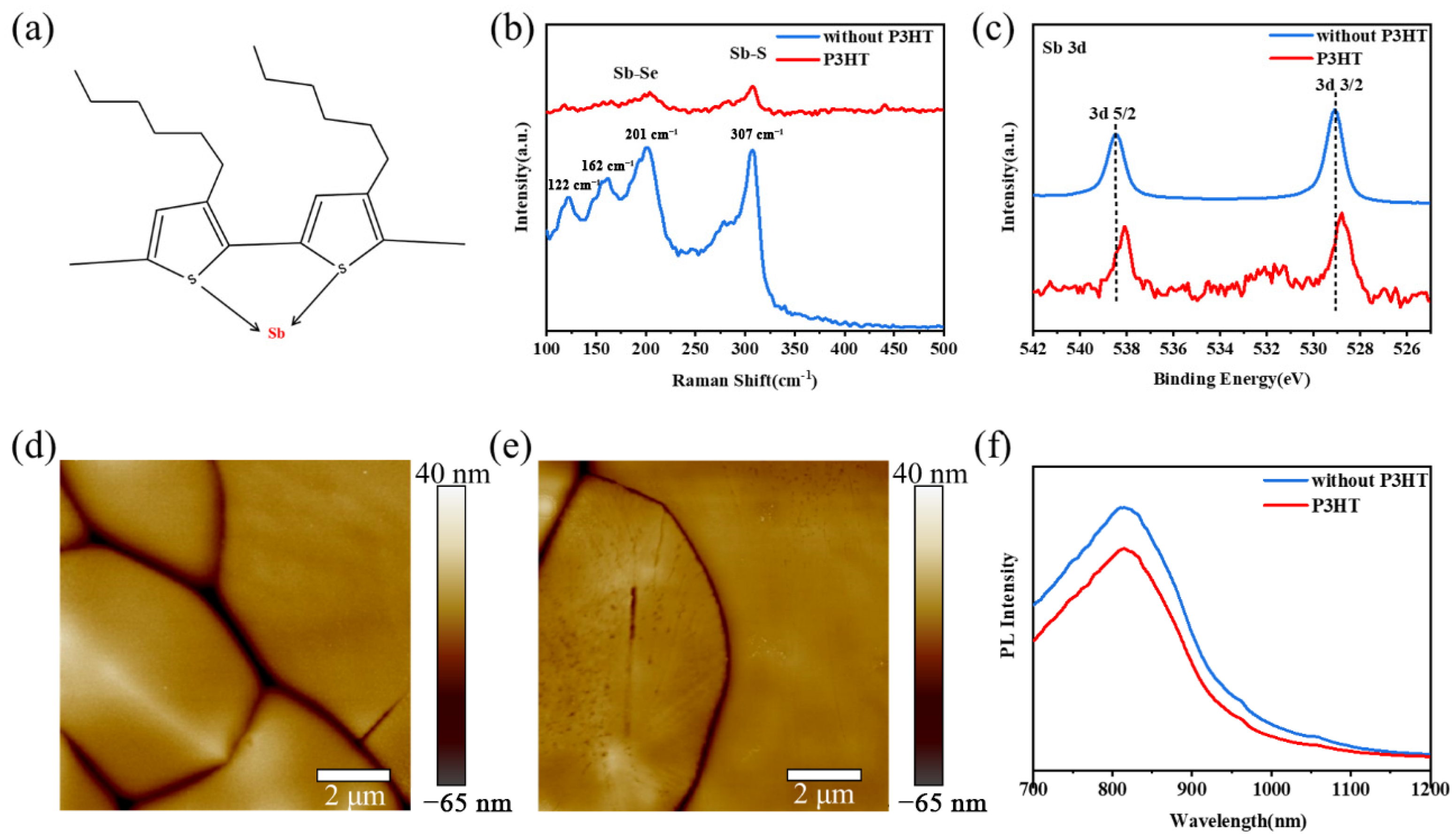
3 film and carbon electrode. As previously reported, the strong chemical interaction between P3HT and antimony chalcogenide poses a potential to essentially promote the charge transfer efficiency (
Figure 5a) [
6]. Raman spectra in
Figure 5b indicate that the Sb
2S
3/Sb
2(S, Se)
3 film shows the characteristic Sb–S bond vibration at around 307 cm
−1, while the peak around 201cm
−1 is recognized as the characteristic Sb–Se bond vibration [
6,
25,
26]. After P3HT had been added to the solar cells, these chemical bonds became weaker, indicating the existence of interfacial interaction. The adjacent thiophene fractions have chelation towards Sb atoms to form a stable compound, which could displace these Sb-chalcogen bonds to passivate the interfaces. X-ray photoelectron spectroscopy (XPS) was also executed to deeply investigate the passivation effect. Compared with the Sb
2S
3/Sb
2(S, Se)
3 film, the Sb 3d peaks of Sb
2S
3/Sb
2(S, Se)
3/P3HT shifted to lower binding energy (
Figure 5c). The low binding energy suggested that the electron density around Sb increased, which could be ascribed to the interactions with electron-rich thiophene fractions [
27].
Atomic force microscopy (AFM) was performed to observe the change in the morphology with and without a P3HT layer (
Figure 5d,e). According to the AFM results, the roughness values (
Rq) of the Sb
2S
3/Sb
2(S, Se)
3 and Sb
2S
3/Sb
2(S, Se)
3/P3HT are calculated to be 12.0 nm and 6.52 nm, respectively. Therefore, the deposition of the P3HT layer reduced the surface roughness of Sb
2S
3/Sb
2(S, Se)
3 films. The flat surface is believed to benefit the interfacial contact with the carbon electrode. In addition, the steady-state photoluminescence (PL) spectra showed that the PL intensity of Sb
2S
3/Sb
2(S, Se)
3 films was smaller than that of Sb
2S
3/Sb
2(S, Se)
3/P3HT films (
Figure 5f). The quenched PL indicated that P3HT significantly enhanced hole extraction of Sb
2S
3/Sb
2(S, Se)
3 based solar cells [
28,
29].
To evaluate the influence of P3HT on PV performance, carbon-based Sb
2S
3/Sb
2(S, Se)
3 solar cells with and without P3HT were fabricated by depositing carbon electrodes on the Sb
2S
3/Sb
2(S, Se)
3 and Sb
2S
3/Sb
2(S, Se)
3/P3HT substrates. As depicted in
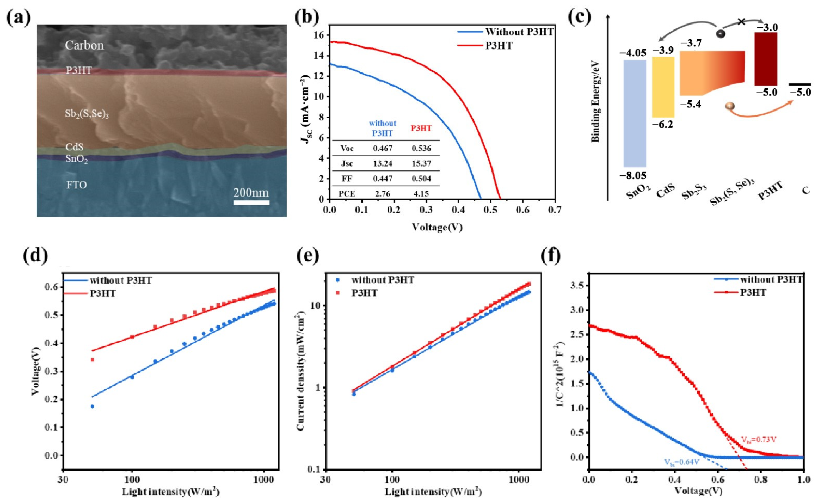
Figure 6a, the carbon electrode closely contacts the P3HT layer, which is favorable for charge collection. In
Figure 6b, the
J–V curves showed that the solar cell with P3HT showed a champion PCE of 4.15%, with a
VOC of 0.536 V,
JSC of 15.37 mA·cm
−2, and FF of 0.504, while the solar cell without P3HT showed a much lower PCE of 2.76%, with a
VOC of 0.467 V,
JSC of 13.24 mA·cm
−2 and FF of 0.447. The energy alignments of the solar cells with a structure of SnO
2/CdS/Sb
2S
3/Sb
2(S, Se)
3/P3HT/carbon are illustrated in
Figure 6c [
20,
29,
30]. The high HOMO of P3HT can effectively prevent electrons from entering P3HT, which remarkably suppressed the recombination at this interface and thus increased the PCE of solar cells.
Figure 6d shows the dependence of
VOC and
JSC on light intensity (
I), which can be fitted by the following two equations [
31].
where
k is the Boltzmann constant,
T is the absolute temperature,
e is the elementary charge, and
ε/
α are the ideality factors of a diode. The
ε for the solar cells with and without P3HT was calculated to be 4.01 and 2.60, respectively, indicating the suppression of the monomolecular trap-assisted Shockley-Read-Hall (SRH) recombination with P3HT [
32]. A linear dependence of
JSC on
I is also found for both devices and the
α values obtained are calculated to be 0.90 and 0.95 for the solar cells with and without P3HT (
Figure 6e), respectively, which demonstrates that P3HT HTM enhanced charge separation and suppressed bimolecular recombination [
18]. Mott–Schottky plots of the different solar cells were also collected. As shown in
Figure 6f, the built-in potential (
Vbi) for the pristine and P3HT devices is calculated to be about 0.64 V and 0.73 V, respectively. The larger
Vbi would contribute to a higher driving force for efficient charge separation and a wider depletion region inhibiting the charge recombination, which is beneficial for achieving higher
VOC and FF, consistent with the
J–V curves. All of the above characterizations are in good consistence with the performance difference between solar cells with and without P3HT.
3. Materials and Methods
3.1. Device Fabrication
Deposition of SnO2 films: All devices were deposited on clean fluorine-doped tin oxide (FTO) glass. FTO glass was cleaned thoroughly in deionized water, ethyl alcohol, and isopropanol with the assistance of sonication. Prior to electron transport layer deposition, the substrates were subjected to UV/ozone treatment for 20 min at room temperature. SnO2 blocking layers were spin-coated onto FTO glass at 3000 rpm for 30 s, using SnO2 colloidal dispersion. All processes were conducted in an ambient air atmosphere.
Deposition of CdS films: CdS thin films were then deposited by a chemical bath deposition (CBD) method. Next, 30 mL of 15 mM Cd (NO3)2 and 39 mL of ammonia water were mixed and stirred for 5 min. Then, 19.2 mL of 1.2 M thiourea and 210 mL of deionized water were added to the mixture and stirred for 2 min to get the precursor solution. Thereafter, the solution was heated and kept at 65 °C by using a water bath. FTO/SnO2 substrates were sloped down in the precursor solution and maintained for 15 min. After the samples were taken out, a 20 mg/mL CdCl2 solution was spin-coated onto the as-deposited CdS layer, followed by annealing at 400 °C for 10 min to get the final FTO/SnO2/CdS samples. All processes were conducted in an ambient air atmosphere.
Deposition of Sb2S3 and Sb2(S, Se)3 films: All Sb2S3 and Sb2(S, Se)3 films were deposited by hydrothermal method.
For the deposition of the Sb2S3 films, 20 mM KSbC4H4O7·0.5H2O and 40 mM Na2S2O3·5H2O were dissolved in deionized water. The mixture was then put into the Teflon tank of autoclave and the FTO/SnO2/CdS substrate was put into the above solution and heated to 135 °C and kept for 10 h using an oven. After cooling down to room temperature, the samples were taken out and washed with deionized water and ethyl alcohol. Then, they were annealed at 350 °C for 15 min in a glove box filled with N2 (1.2–1.5 mbar).
For the deposition of Sb2(S, Se)3 films, 20 mM KSbC4H4O7·0.5H2O and 80 mM Na2S2O3·5H2O were dissolved in deionized water. After the two chemicals were dissolved, 4 mM of selenourea was added to the solution and stirred until it was well dissolved. The mixture was then put into the Teflon tank of autoclave and the FTO/SnO2/CdS substrates were put into the above solution. The hydrothermal process was conducted by putting the solution in an oven at 135 °C and kept for 3 h. After cooling down to room temperature, the samples were taken out and washed with deionized water and ethyl alcohol. Then, they were annealed at 350 °C for 15 min in a glove box filled with N2 (1.2–1.5 mbar).
For the deposition of Sb2S3/Sb2(S, Se)3 films, a two-step hydrothermal method was developed. Firstly, the Sb2S3 films were deposited by the above hydrothermal method and deposition duration was adjusted to 1 h, 2 h, 3 h, and 4 h. After the deposition of Sb2S3 films, Sb2(S, Se)3 films were also deposited by the hydrothermal method and the reaction duration was fixed to 2 h. After hydrothermal deposition, the above films were taken out and washed with deionized water and ethyl alcohol. Then, they were annealed at 350 °C for 15 min in a glove box filled with N2 (1.2–1.5 mbar).
Deposition of P3HT films: P3HT solution was prepared by dissolving 10 mg/mL P3HT in chlorobenzene. The P3HT layer was deposited on the Sb2S3/Sb2(S, Se)3 films by spin-coating the P3HT solution at room temperature with 3000 rpm for 30 s. Finally, the deposited samples were annealed at 120 °C for 10 min. All processes were conducted in a glove box filled with N2 (1.2–1.5 mbar).
Deposition of carbon electrodes: Carbon electrodes are deposited on different films by using a commercialized carbon paste that was purchased from Guangzhou Seaside Technology Co., Ltd. and was used without any treatment. The wet carbon layers were first painted on the targeted films at room temperature, which were then annealed at 120 °C for 30 min to form the final carbon electrode. All processes were conducted in a dry-air atmosphere.
3.2. Characterizations
XRD patterns were obtained on a Rigaku D/MAX-2500 X-ray diffractometer with an X-ray tube Cu Ka radiation. (λ =1.5406 Å). Ultraviolet-visible-infrared spectrophotometer absorption spectra were recorded on a Shimadzu UV-3600 ultraviolet-visible spectrometer. SEM images and EDS were obtained on a SUPRA55 SEM at an accelerating voltage of 10 kV. The surface roughness of the films was characterized by a Bruker Dimension ICON AFM. Raman spectroscopy was measured at room temperature using a Raman spectrometer (InVia, Renishaw Inc., Stonehouse, UK) equipped with a green laser (532 nm), and the laser power and objective were 50 mW and 50×, respectively. The chemical states of the film surface were evaluated by an X-ray photoemission spectroscope (ESCALab250Xi). Steady-state PL spectra were recorded on a Nanolog FL3-2iHR (Horiba Jobin Yvon Ltd., Palaiseau, France) with an excitation wavelength of 635 nm.
The photovoltaic performance was tested under a solar light simulator (Newport Oriel Sol 3A, model number 94063A, AM 1.5 global filter) in an ambient air atmosphere. The light intensity was calibrated to 1 Sun (100 mW/cm2) using an Oriel reference solar cell (monocrystalline silicon) and meter. The active area of cells was masked at around 6.25 mm2. Current density-voltage (J–V) curves, the dependence of JSC and VOC on the light intensity, and Mott-Schottky curves were measured on a ZENNIUM pro electrochemical workstation (ZAHNER-Elektrik GmbH & Co., KG, Kronach, Germany) in an ambient air atmosphere.
