1. Introduction
LiDAR is widely used in autonomous cars [
1], unmanned aerial vehicles (UAVs) [
2], and forest science [
3]; it sends out a pulse laser signal and simultaneously gathers the information of the reflection from objects. The object distance is calculated by the optical time-of-flight (TOF) [
4], thus the higher the laser peak current, or power, pulses means farther detection can be achieved, and shorter pulse duration represents better detection accuracy. For some applications, such as simultaneous localization and mapping (SLAM) [
5], we additionally need a high measurement sampling rate to acquire enough information.
Two laser driver topologies, including the laser diode being in parallel [
6] and series [
7] with a transistor, have been introduced in the literature. The series topology is featured with a simple circuit, whereas the parallel one is characterized by high optical power and short pulses [
8,
9]. Some researchers integrated the power switch with its driver using CMOS technology in order to operate at megahertz frequency [
7,
10]; however, high switching frequency leads to more switching loss for conventional silicon-based materials. The methodology introduced in [
11] uses a momentary boost in supply voltage to reduce power overhead and thus improves the power efficiency. Furthermore, some other researchers [
12,
13] used wide bandgap devices such as the GaN HEMT for the laser driver application due to their low products of total gate charge and conduction resistance. The wide bandgap devices implemented in laser drivers yield better compactness and power efficiency than that of MOSFET [
13]. In recent years, EPC Co. have published a laser driver with an enhancement mode power GaN device that is capable of driving a laser with current pulses, with total pulse widths as short as 1.2 ns and currents of up to 28A [
14].
Aside from the aforementioned advantages, GaN devices have other superior material properties, such as zero reverse recovery and low output capacitance difference between turn-on and turn-off of the transistor [
15,
16]. There are also challenges using D-mode GaN, for example, a negative voltage is required to be applied at the gate to turn off the normally on channel. To overcome the aforementioned challenges, several schemes [
17,
18,
19] have transformed the normally on device into a normally off transistor with the charge pump gate drives [
17], the cascode GaN structure [
18], and the self-powered gate drives [
19]. As the laser driving frequency is limited by the inductance of the laser and the capacitance of the driver system, we will need to reduce the parasitic inductance on the circuit board and use GaN HEMT to reduce the parasitic capacitance for higher repetition rate and shorter pulse duration [
6].
In addition, high power laser emitters are critical to the LiDAR system, of which VCSEL is used mostly in high speed optical applications such as 3D sensing and light detection and ranging [
20,
21]. With large current density, directive emission, low divergence angle, narrow bandwidth, and low power consumption, VCSEL has become one of the most reliable and high performance lasers [
22,
23,
24]. Some studies about the analysis of laser equivalent circuit models [
25,
26,
27,
28] considering the resonance mechanism [
25], rate equations [
26], contact resistance equation [
27], and thermal equation [
28] can yield simulation results approaching the real phenomenon.
The aim of this paper is to propose a laser driver with D-mode GaN HEMT that is capable of generating high peak power pulse within nanoseconds to VCSEL for a LiDAR system. With feedback control of pre-boosted supply voltage, the presented laser driver will yield high peak power under high power efficiency.
Section 2 depicts the laser diode and the VCSEL equivalent circuit model used in this research according to rate equations and the resonance phenomenon. In
Section 3, the proposed high power laser driver for VCSEL is discussed, including pre-boosted power supply and analysis of laser circuit response. The design guide for the D-mode GaN based laser driver that provides power to light efficiency improvement and high peak power is presented in
Section 4. The proposed laser driver with D-mode GaN and VCSEL is verified through the PSPICE simulation and experiment. The estimation of total power received by the photodetector is shown in
Section 5. The conclusion of this work is summarized in
Section 6.
2. Laser Diode
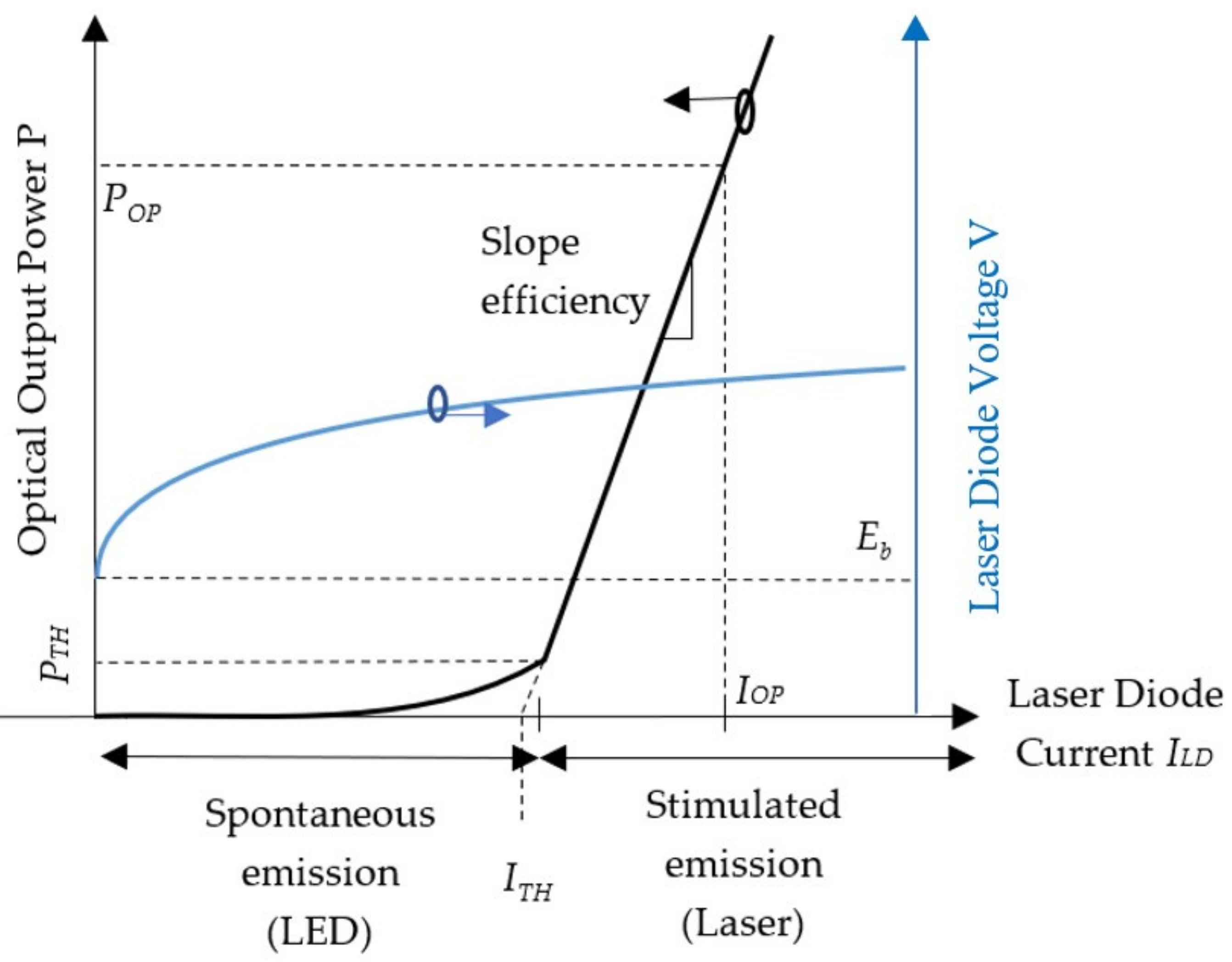
For the circuit analysis and simulation laser diode driving, we need to obtain the circuit response instead of the laser response. Thus, the equivalent circuit needs to be used to predict the waveforms of the current and voltage using circuit simulation software. As shown in
Figure 1, within the maximum power rating region, the P-I curve distinguishes the spontaneous emission (LED light emitting) region from the stimulated emission (laser oscillating) region; the current level that triggers laser oscillation is the threshold current. The slope efficiency is almost constant in the stimulated emission region.
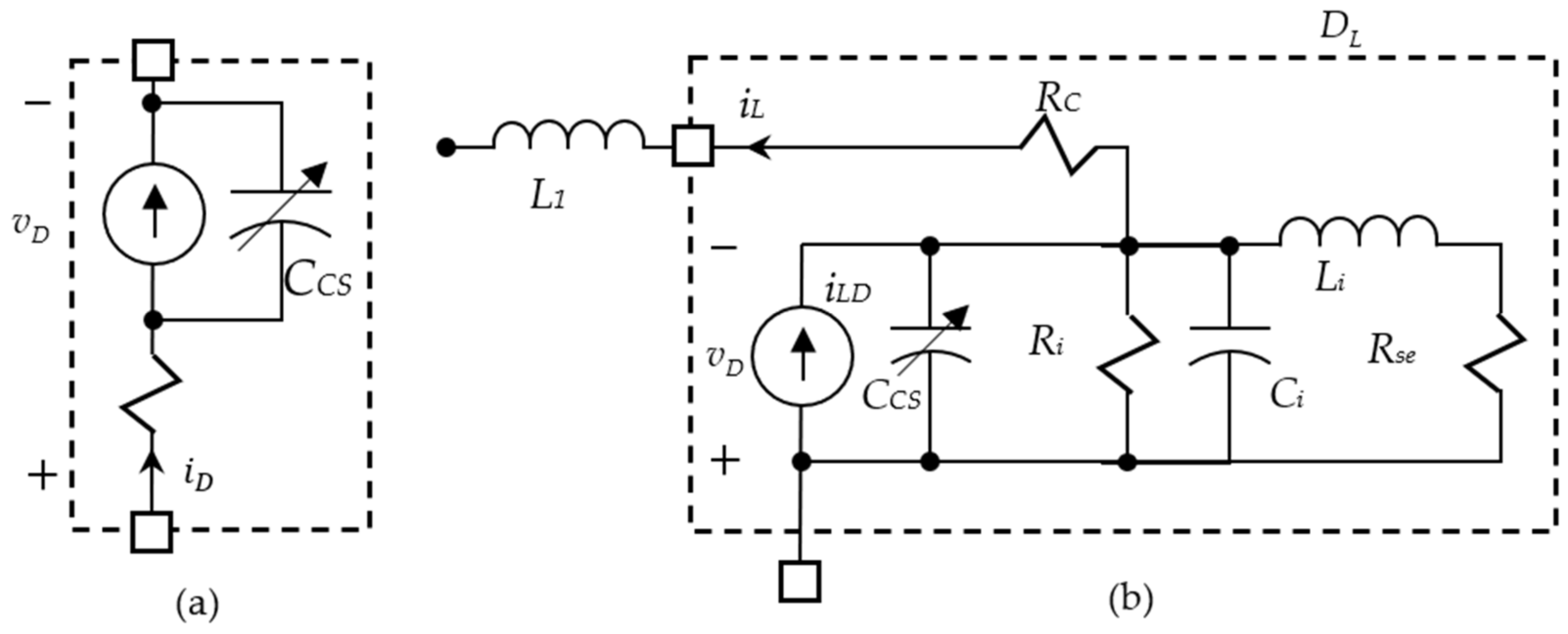
As shown in
Figure 2, the major term of the current source of the PIN diode [
27] can be modeled into a temperature dependent function as follows.
Table 1 shows the parameters used in circuit analysis, which includes different stray inductances when using matrix board and printed circuit board (PCB).
where
Eb denotes band gap potential of the semiconductor in volts,
n denotes temperature exponent, and
A is a constant independent of the temperature
T. It is modelled into a similar form as a normal PN diode as follows.
It may be substituted with
N = 1 and the reverse saturation current as follows.
where
Eb denotes the band gap potential of the laser diode in volts. This capacitance named the space-charge capacitance,
CSC, of the active region is given as follows.
where
Csc(0) is the zero-bias space-charge capacitance and
VJ is the heterojunction built-in potential. The active layer diffusion capacitance of the laser diode is
Ci. The inductance
Li arises from the small signal analysis of the rate equations and represents the resonance phenomenon of the laser diode with capacitance
Ci. The resistance
Ri includes the differential resistance of the laser diode model damping due to the spontaneous and stimulated recombination terms in the rate equations. The resistance
Rse models damping due to spontaneous emission coupled into the lasing mode. In the equivalent circuit we model both
Ri and
Rse together into
Ri,se;
Rc is the contact resistance, which includes the semiconductor bulk resistance. The main contribution to
Rc comes from the contacts because the bulk resistance of semiconductors is very low. The inductance
L1 arises from the circuit parasitic inductance, which is always preferred to be as low as possible.
3. VCSEL Laser Diode Driver
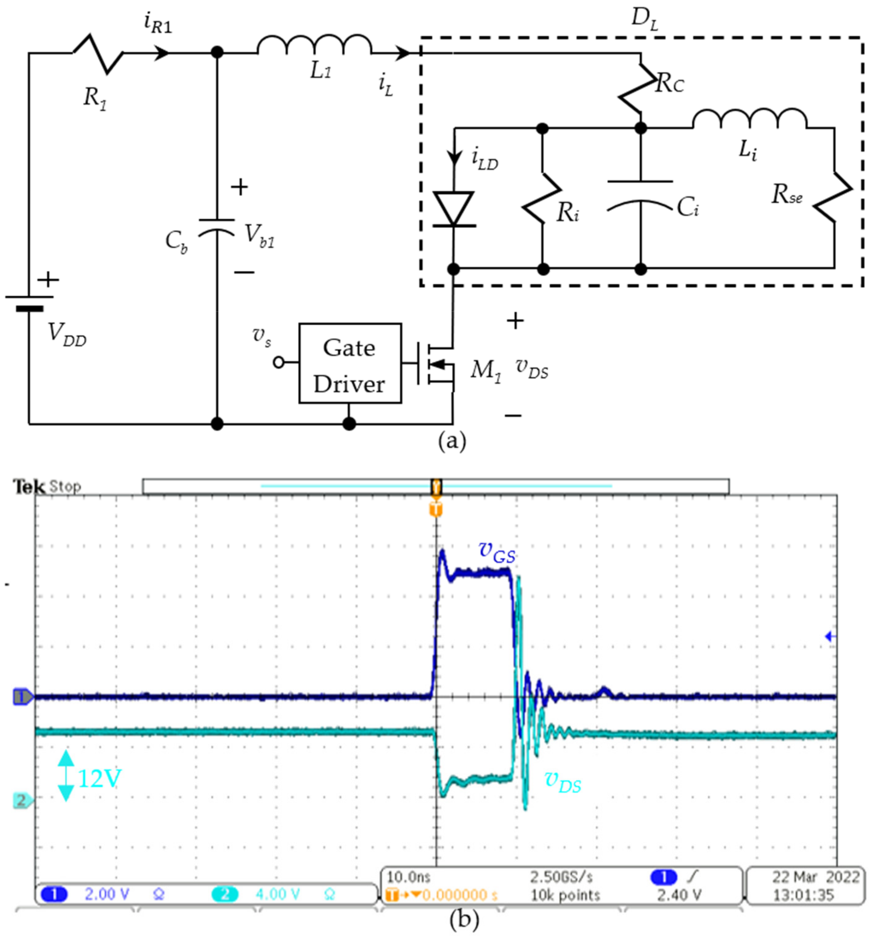
Commercial circuitry to switch on the laser is EPC9144 [
14], which is simplified as shown in
Figure 3a. The capacitor
Cb is 1 nF, which serves as a line filter. When
vGS is high, the transistor
M1 turns on, and the current flows from the voltage source through a very small resistance
R1 to the laser diode. The reverse saturation current
Iss on the laser diode is a function of temperature when the temperature of the laser diode increases the diode current
iLD derived in Equation (1) and cannot be ignored [
27] at a constant temperature operation. The moment when
vDS goes to zero is the time when the laser diode goes into the stimulated emission mode, and the rest of the oscillating response is the resonance phenomenon of the laser diode when the laser diode is likely to be in the spontaneous emission mode. The signals are taken from the transistor as shown in
Figure 3b. When the gate-source voltage is operated with an on-time duration 10 ns at a pulse repetition rate 10 kHz, the transistor
M1 turns on and
vDS drops to low voltage. The actual
iLD can be roughly estimated through dividing the voltage difference
VDD −
vDS by the dynamic
Ron resistance of the GaN HEMT.
The drawback of the circuit in
Figure 3a is the resistor
R1 must be high enough to reduce the voltage ringing, as shown in
Figure 3b, when the transistor
M1 turns off. The high resistance
R1 limits the current
iLD flowing through the diode, which is typically ten times higher than the contact resistance
Rc. For the high peak laser power application, the circuit must be reconsidered.
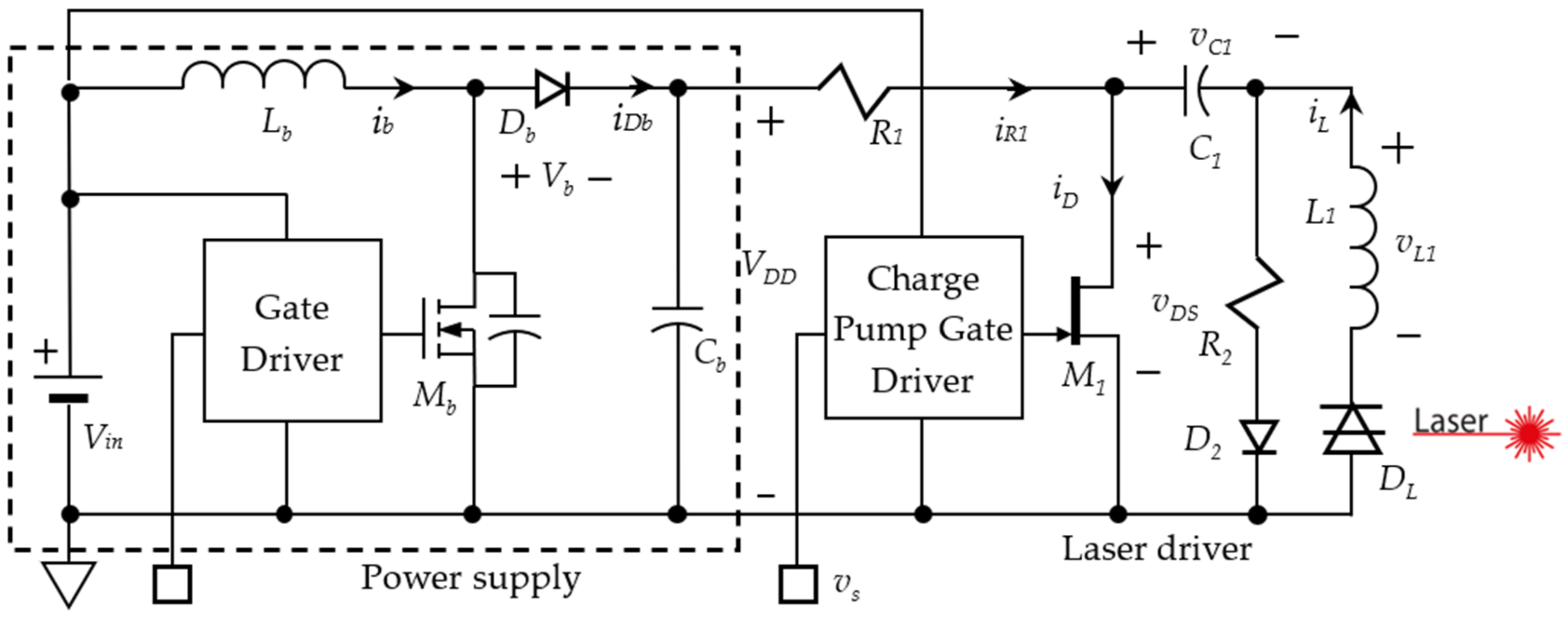
3.1. The Proposed VCSEL Laser Diode Driver
There is a need to adjust the current level of driving due to different selections of lighting in a number of groups of laser diodes. Therefore, a boost converter used to escalate the voltage level of the capacitor is proposed and shown in
Figure 4.
3.2. Power Supply
The boost switching power supply is used to control the input voltage
vDD for the laser driver circuit from a low voltage, such as
Vin = 4
V from Li-ion battery. The boost power supply is used to boost the low voltage into a high voltage for the laser. The input voltage
vDD is then subsequently charging the capacitor
C1, which is the main voltage source in the laser lighting loop. On the power supply side, the boost converter circuit consists of an inductor
Lb, diode
Db, transistor
Mb, and capacitor
Cb. The diode
Db comes into the reverse bias when the transistor
Mb is switched on. During the
Mb turn-on period
δbTb, the inductor
Lb increases its magnetic energy with a current rise as follows.
This magnetic energy will be conveyed to the capacitor
Cb during its
Mb turn-off period. Because the output current from the power supply to the laser driver is very low, the boost converter working in the discontinuous current mode is assumed. On the path of the current flowing from the inductor
Lb to the capacitor
C1, the diode
Db is forced into a forward bias. The charging current of the capacitor
Cb is derived in the steady state as follows.
where α, 0 ≤ α ≤ 1, denotes the fraction of the current flowing time from the
Mb turn-off period
. During the
Mb turn-off period, the current
iDb flows into the capacitor
Cb through the diode
Db.
The term
VDD denotes the average voltage across the capacitor
Cb;
IR1 denotes the average current flow through resistor
R1;
PL denotes the power loss in the laser diode driver including the resistor
R1. Substituting Equation (7) into (6) and comparing Equations (5) and (6), we have the capacitor voltage
vDD as follows.
It is observed that the capacitor voltage is irrelevant to the capacitance when the boost converter stands alone. However, when we considered the current output
iR1 from
R1, the capacitor voltage
vDD is charged/discharged by two sources, and the total voltage can be calculated from the superposition theorem as follows.
The capacitor voltage is then a function of the capacitance of
Cb and the charge withdrawn Δ
Q from the capacitor. On the laser driver side, the capacitor
C1 obtains the charges from capacitor
Cb when transistor
M1 turns off. The charge redistribution between two capacitors occurs when transistor
Mb turns on, and the diode
Db is under reverse bias.
The steady state of
vC1 is obtained when the charge redistribution is completed. The time constant may be seen as the capacitor
Cb to charge the
C1, which, relatively, has a very small capacitance. The governing equation for the charge redistribution is derived as follows.
In order to reduce the complexity for the analysis, one may reduce charging time constant
T1 of capacitor
C1. The capacitor loses electrical energy Δ
E each time when the laser diode is powered up within the pulse train period
Tpp. Assuming that
at steady state, we can derive the power loss from the laser diode driver circuit as follows.
Equation (8) is then written as follows.
The above equation states that the power supply duty cycle δb is proportional to the square root of the voltage drop ΔvC1 in capacitor C1.
3.3. Laser Circuit Response
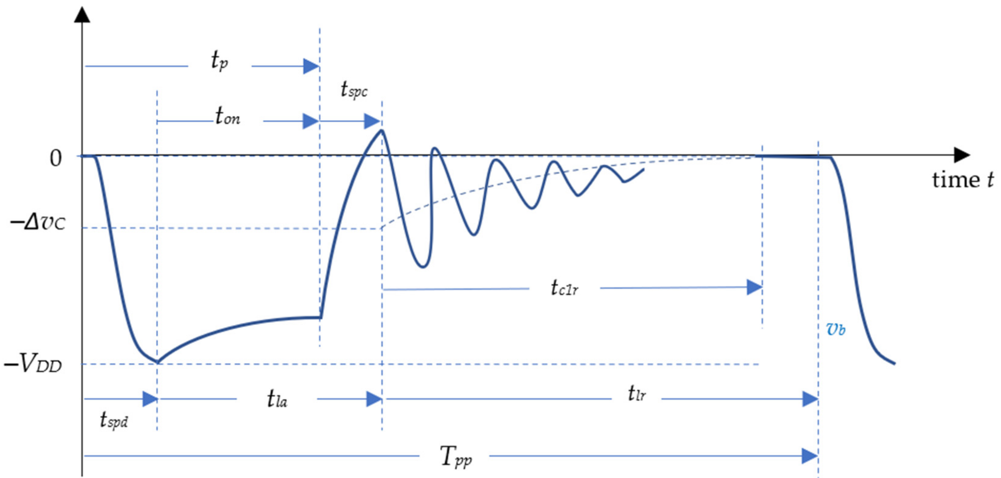
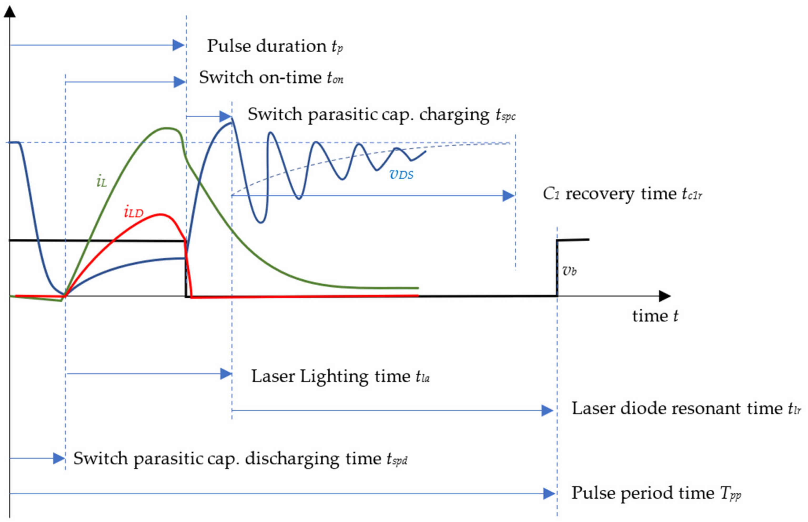
The fundamental data of the VCSEL are from a light–current–voltage (LIV) curve, which simultaneously measures the electrical and optical output power characteristics of the device. LIV characteristics are a function of laser temperature as indicated in Equation (6), which must be tightly controlled. The main reasons for performing low-duty-cycle pulsed laser driving are thermal management, thermal response, and transient response. The pulse driving technique is mainly applied to generate nanosecond pulses of high peak power with solid-state bulk lasers. In this study, we are especially interested in the repetition rate of 10 kHz and 1 MHz. As shown in
Figure 5, there are four phases in a LIV pulse, namely the switch parasitic capacitor discharge time
tspd, the switch on-time
ton, the switching parasitic charge time
tspc, and the laser diode resonant time
tlr. The entire cycle between two consecutive gate turn-on signals is a pulse period time
Tpp, which is the reciprocal of the laser repetition rate.
where
Tpp is the reciprocal of the repetition rate
fLD, that is
The pulse duration achieved is typically in the nanosecond range and usually well above the resonator round-trip time. The pulse duration of the laser pulse is
tp, which consists of the switch parasitic capacitor discharge time
tspd, the switch on-time
ton.
As a simplified model, the laser lighting time driven by the switch conduction is written as follows.
The power of the laser radiation builds up very quickly in the laser resonator. The large cavity power present at that time leads to further depletion of the stored energy during the time where the power decays. Usually, the energy extracted after the pulse maximum is similar to that before the pulse maximum, and the resulting pulse shape is roughly symmetric. The laser diode resonance is due to inductance
Li with capacitance
Ci. The resonance mechanism of a true laser diode may be more sophisticated than the circuit model, however, it is simplified into the circuit as shown in
Figure 2 and analyzed only for circuit control purposes.
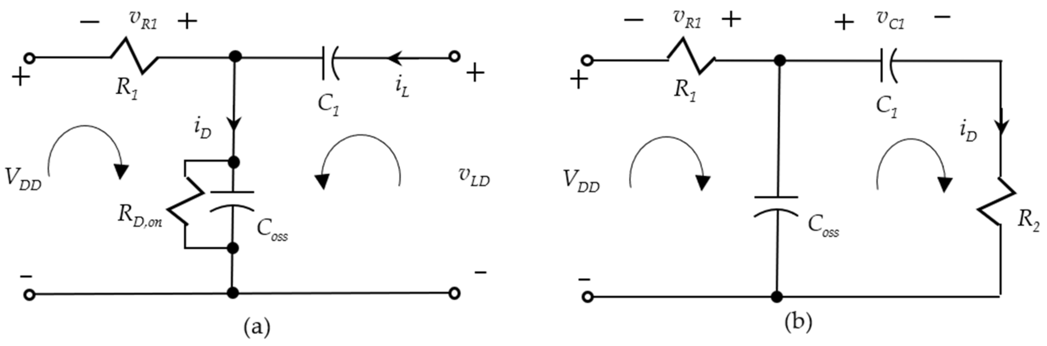
3.3.1. Switch Parasitic Capacitor Discharge Time tspd
As shown in
Figure 6, at the moment after
vs turns to high voltage for switching on the transistor
M1, the parasitic capacitors in
Coss are discharged in order to bring the transistor
M1 to the linear ohmic state. The capacitors
Coss discharge through the laser diode
DL and the inductor
L1 with the governing equation as follows.
In the above equation, the natural frequency
ωspd is a function of inductor
L1 and capacitor
Coss as follows.
The parallel resistance
R2 can be ignored because the on-resistance of the GaN device is much smaller than
R2. However, the parallel resistance
R2 may yield a current path when the laser diode starts to flow and thus weaken the laser diode current. Therefore, we may add an extra diode to prevent
R2 current from flowing in the same direction as the laser diode. The damping ratio of the current oscillation is as follows.
where
Rc is the contact resistance of the laser diode. The discharging is under a very light damping, hence the rise time of the current response, i.e., the discharging time, is estimated as follows.
According to the parameters of the inductance, parasitic capacitance, and the resistance provided as shown in
Table 2, the capacitor discharging time together with the gate drive delay is, in total, around 1 ns. The switch parasitic capacitor discharge time
tspd forms a barrier for the laser current to flow; that is, the pulse duration shall not be smaller than
tr,spd in order to have the laser diode come to its stimulated emission.
3.3.2. Switch On-Time ton
During the switch on-time, the switch conducts the current from the capacitor
C1 through the laser diode
DL and the inductor
L1 to the transistor
M1 with the governing equation as follows. It is assumed that the diode holds a constant voltage
VLD,on depending on the
ISS of the laser diode. It may also be considered that the capacitor
C1 charges both the inductor and the on-resistance of the transistor
RD. Assuming the on-resistance of the transistor
RD is small and the damping ratio
is negligibly small, the governing equation is derived as follows.
In the above equation, the natural frequency
ωon is a function of inductor
L1 and capacitor
C1 as follows.
Substituting the initial voltage of
vC1 as
into Equation (22), we obtain
The capacitor voltage of
vC1 is reducing along the time when the transistor
M1 is on, and the lost voltage of the capacitor will be refilled during the
M1 turn-off time. The capacitor voltage drop when ignoring
VLD,on is derived as follows.
The energy loss in the capacitor
C1 is mainly consumed by the laser diode, hence the power transferred to the laser diode for the lighting pulse is then derived as follows.
The maximum power that can be transferred for each pulse can then be derived from taking the first derivative of the above equation.
One trivial solution of the above equation is
ton = π/
ωon, that is, the electrical energy stored in the capacitor is used up during each pulse of laser switching. The inductor current
iL1 is then derived in terms of the capacitor voltage as follows.
Although all current of iL flows through the laser diode, only a portion of the current becomes the lighting current iLD stated in Equation (1). The fraction between iLD and iL during the on-time is mainly a function of the resistance Ri, including the differential resistance of the laser diode model damping due to the spontaneous and stimulated recombination terms in the rate equations. The larger the resistance Ri, the higher the lighting current iLD is. The other current branch of the laser diode includes the current path through the inductance Li, representing the resonance phenomenon of the laser diode, the resistance Rse, representing damping due to spontaneous emission coupled into the lasing mode, and the current through the active layer diffusion capacitance of the laser diode Ci. The resonance phenomenon and the active layer diffusion will prolong the current of iL after the lighting current iLD cuts off from the diode equation.
The significance of this proposed circuit, obtained from Equation (22), is that there is no other resistor presented on the path of the laser diode lighting during the switch turn-on time. The damping ratio of the lighting current is subjected only to the dynamic on-resistance of the transistor M1. When the on-resistance RD of the transistor is made very small, the maximum light current is proportional to the VDD and not limited by the resistance in the current loop.
3.3.3. Transistor Parasitic Capacitor Charge Time tspc
As shown in
Figure 6, at the moment after
vs turns to low voltage for switching off the transistor
M1, the parasitic capacitors in
Coss shall be charged in order to bring the transistor
M1 to the off-state. The capacitors
Coss are charged through the laser diode
DL and the inductor
L1 with the governing equation as follows.
In the above equation, the natural frequency
ωspc and
are the same as
ωspd and
derived in Equations (19) and (20), respectively. The charging is under a very light damping, hence the rise time of the current response, the charging time, is the same as derived in Equation (21). The only difference between charging and discharging of the parasitic capacitors is that the laser diode is conducting current
iLD during the charging time only.
During the same time, the current keeps flowing to drain out the zero-voltage junction capacitor of the laser diode, as shown in
Figure 5.
3.3.4. Laser Diode Resonant Time tlr
In the case where the GaN HEMT transistor
M1 turns off at the time
tr,spc passed the
vs turn-off time, then the output parasitic capacitor
Coss of the transistor
M1 has been filled up; however, the resonance through the same capacitor as the current in the inductor has no zero first-derivative.
The value of
R2 is mapped into the dynamic impedance
Z2 from the parallel connection with
L1 and
Coss into a series connection as follows.
When the GaN HEMT transistor
M1 turns off, the parallel resistance
R2 can contribute to the damping ratio. The damping ratio
when
RC +
Rse =
Z2 is then written as follows.
The damping ratio is preferable to be critical damping without causing too much turn-off overshoot voltage on
vDS.
Table 3 shows the
R2 adjusted according to the damping desired.
3.3.5. C1 Recovery Time
There is another important time that determines the repetition rate of the laser diode switching: the capacitor
C1 recovery time. The recovery time is critical when the repetition rate increases, thus for the same pulse duration, the duty of the transistor switching increases. The supply of charges from resistor
R1 through the path from
R1 to
C1 and then to
R2 is activated only when the transistor turns off. The loss of charges from
C1 during the transistor turn-on time must be refilled through its turn off time in order to maintain the capacitor
C1 at the same voltage as the voltage source v
s. The time constant for the charging
Tc1 can be obtained from the
RC charging equation as follows.
The capacitor C1 recovery time tc1r may be estimated as four times the time constant Tc1, which is nearly 98% of the full voltage to VDD.
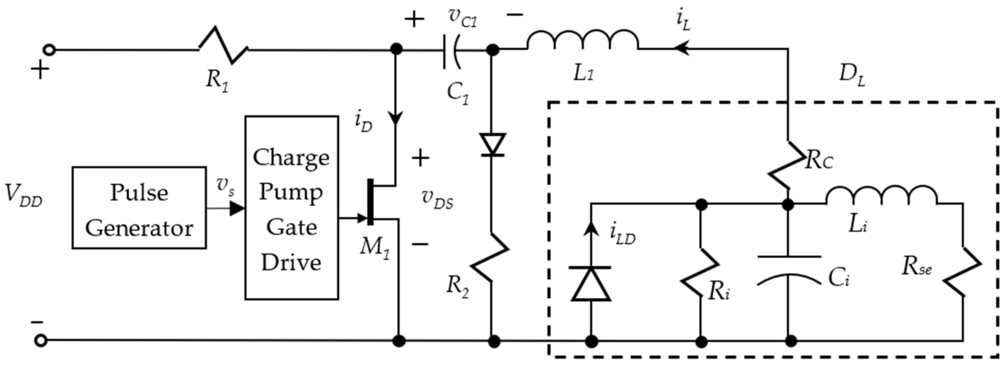
3.4. Sensing the Laser Diode Current
In the small pulse duration or high repetition rate applications, it is difficult to directly measure either the current
iD or the voltage
vDS without interfering with the laser driver circuit. However, the state sensing is of extreme importance during the feedback control of the laser power. In
Figure 7, we simplified the laser driver circuit from the view of resistor
R1. The resistor voltage is labeled in the opposite way such that it matches the wave form of the supposed
vDS. In
Figure 7a, the total laser diode current
iL can be obtained from the branch current solution as follows when
is assumed.
In the above equation, the input voltage
VDD is controlled through the power supply, the voltage
vR1 is sensed, and the dynamic-on resistance of the transistor is assumed. In
Figure 7b, the supplement voltage to the capacitor
C1 is estimated.
The recovery time to time constant ratio m is suggested to be 4, as stated previously, when the 2% voltage error is considered to be the settling time clearance. The average voltage on the resistor R1 can be estimated by taking the average of the integration.
Figure 8 shows the standard voltage response template on resistor
R1. With the voltage response, we can easily label the timing of the individual states of the laser driving process. The anomaly cases include:
- (a)
Due to either the resistance of R1 being too high or the capacitance C1 being too small, the voltage of vR1 is below zero voltage all the time during the high repetition rate operation.
- (b)
The voltage of vR1 does not fall to ─VDD during the short pulse duration operation.
- (c)
Due to either the damping of the laser driver circuit being too high or the charge pump gate drive being subjected to high gate resistance, the voltage of vR1 does not oscillate during the laser diode resonant time tlr.
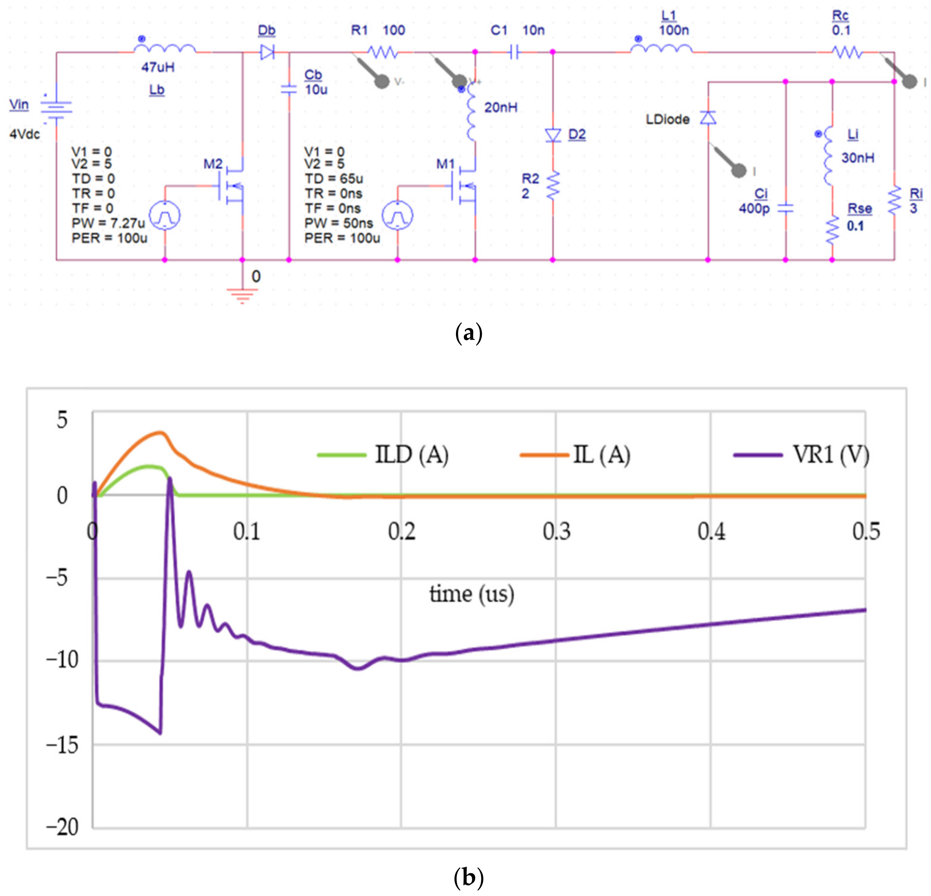
5. Simulation and Experiment
The laser diode SPICE model is based on the laser diode model specified in
Table 1. The boost power supply on the left part of the PSPICE circuit model, shown in
Figure 9a, is so operated that the
VDD shown in capacitor
Cb is 15 V while the simulation result for
tp = 50 ns at its steady state is shown in
Figure 9b. There is a parasitic inductance due to bonding connected in series with the transistor
M1. The parameters used in the simulation as experiment as well are shown in
Table 5. The
ωon derived in Equation (23) is also calculated and converted to 5 MHz, as shown
Table 5. The maximum pulse duration
tp,max is calculated from Equation (41) as 100 ns. The pulse duration
tp = 50 ns is half of
tp,max = 100 ns; one half of total electrical energy previously stored in the capacitor
C1 was released during the laser light process. Therefore, the Δ
vC1 is calculated as 0.3
VDD = 4.5 V from Equation (25) when the switch parasitic capacitor discharge time
tspd is negligibly small and
ton ≈
tp. The simulation result shows, in
Figure 9b, the voltage
vR1 (purple curve line) measured on the resistor
R1 goes from 0 V at 0 s representing the
M1 turn-off state, immediately drops down to −
VDD representing when the transistor
M1 turns on, then jumps to 0 V again at 50 ns, indicating the transistor has been turned off again, and later falls back to the voltage −(
VDD − Δ
vC1) = −10 V at 150 ns, which is inconsistent with the result predicted in Equation (25). For a shorter pulse duration, say, one-tenth of 100 ns (
tp,max), the repetition rate can be as high as 10 MHz.
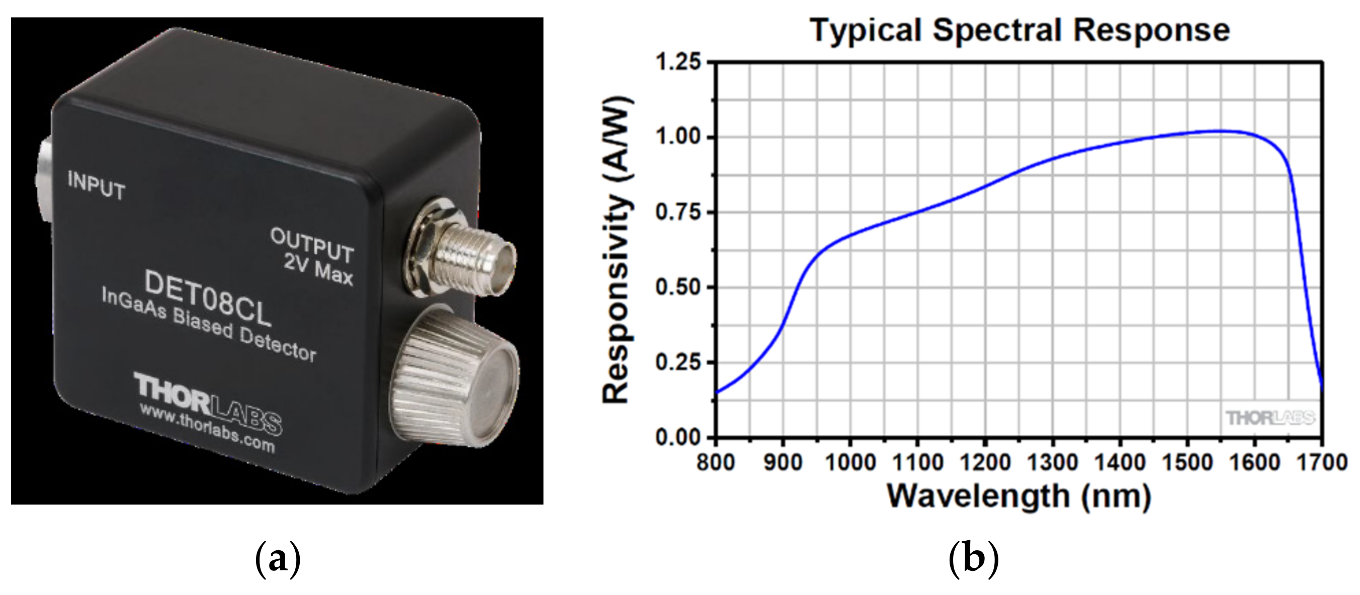
For estimating the output power of a laser diode, the photodiode detector DET08CL(/M) is used, which is an InGaAs junction photodiode (an intrinsic device), and a 50 Ω terminator is used in conjunction with a 50 Ω coaxial cable in our measurements. It behaves similarly to an ordinary signal diode, but it generates a photocurrent when light is absorbed in the depleted region of the junction semiconductor. It determines the expected level of the output current (
IOUT) and the responsivity based upon the incident light.
The definition of photodiode responsivity
R(λ) = IPD/P is the ratio of generated photocurrent
IPD to the incident light power
P at a given wavelength
λ. According to the response curve, the photodiode responsivity
R(λ) is around 0.6 A/W at wavelength 940 nm. Ignoring the dark current (
IDARK), junction capacitance (
CJ), and the other electric characters in the circuit, the received power can be carried out via measured photocurrent (
IPD) at wavelength 940 nm.
To estimate the total out power of the laser diode, the diverging solid angle of the laser beam is checked, and the solid angle of the photodetector is calculated from the active area diameter. The solid angle of a cone with its apex at the apex of the solid angle, and with the full divergence angle 2
θ, is the area of a spherical cap on a unit sphere. The value of
θ defined in this paper is the half angle of the beam plane.
For the PCSEL L13395-04 (HAMAMATSU), its beam spread angle is only 1 degree when its operating power is around 150 mW, . For a 940 nm VCSEL V3-7-2000-S (EGISMOS), its beam spread angle along the wide axis is 60 degrees and is 45 degrees along the narrow axis, .
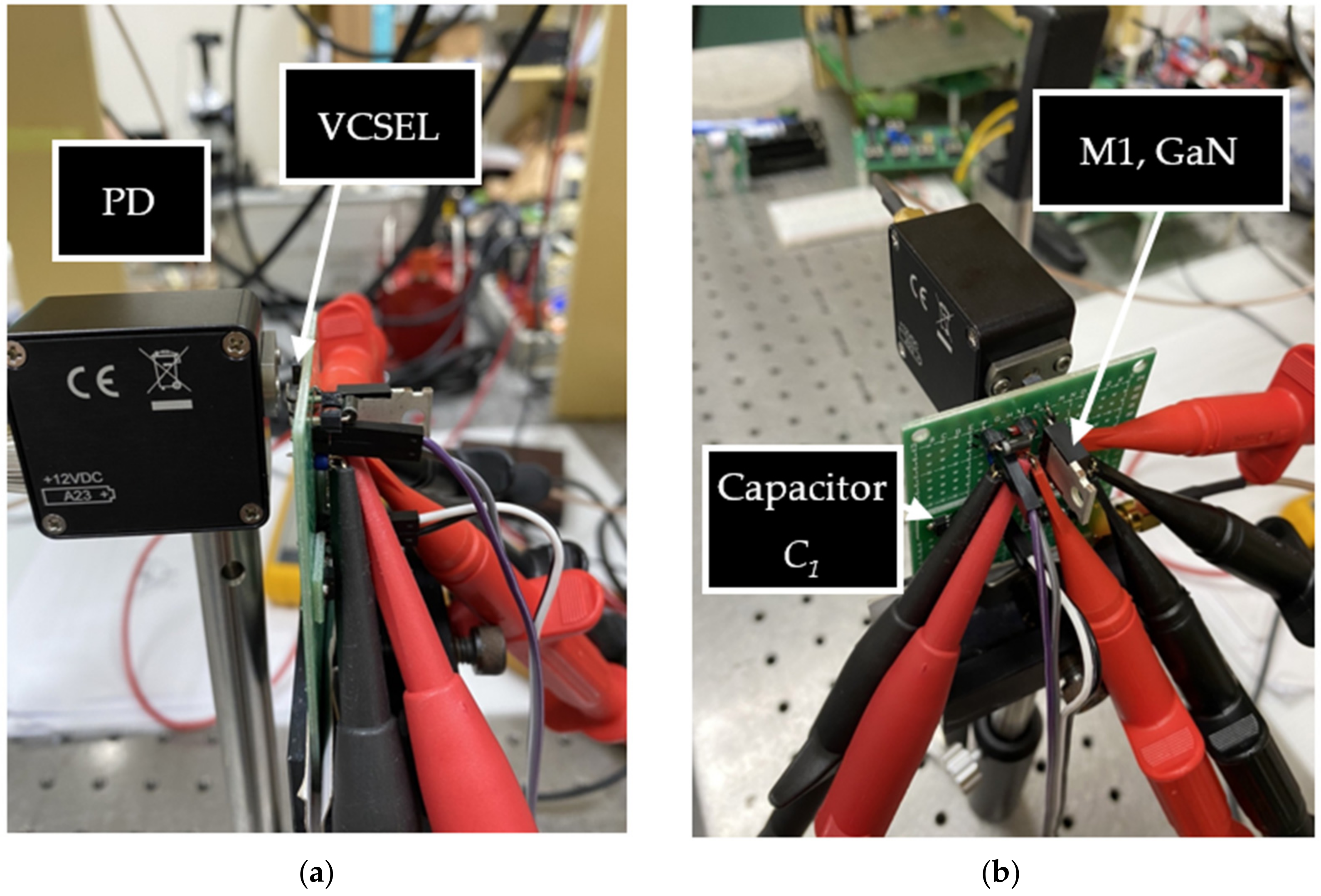
The photodiode detector for the experiment and the experimental setup are shown in
Figure 10 and
Figure 11, respectively. In the experiment, we used the 940 nm VCSEL fabricated in the Department of Photonics at NYCU. The
VDD in this experiment is 15 V. The prototyping board is used in the experiment, and the parasitic inductance
L1 is approximately 100 nH according to the model fitting of the frequency response using Equation (22). The thickness of the prototyping board is 1.55 mm. The spacing between the VCSEL and the photodiode detector is 5 mm, which can also be observed from the
Figure 11a side view to compare the thickness with the distance. The active area diameter of the DET08CL(/M) InGaAs junction photodiode is
Ø80 µm, and its received solid angle was calculated as follows when
.
The power correcting factor for a 940 nm VCSEL V3-7-2000-S is around 300. As for the PCSEL L13395-04, the estimated received power does not have to be corrected because its divergence solid angle is smaller than that of the DET08CL. The D-mode GaN HEMT is used in the experiment, as shown in
Figure 11b, as the transistor
M1. We used a 10 nF capacitor
C1 to produce a
tp,max = 100 ns pulse, which is inconsistent with the simulation. The result is shown in
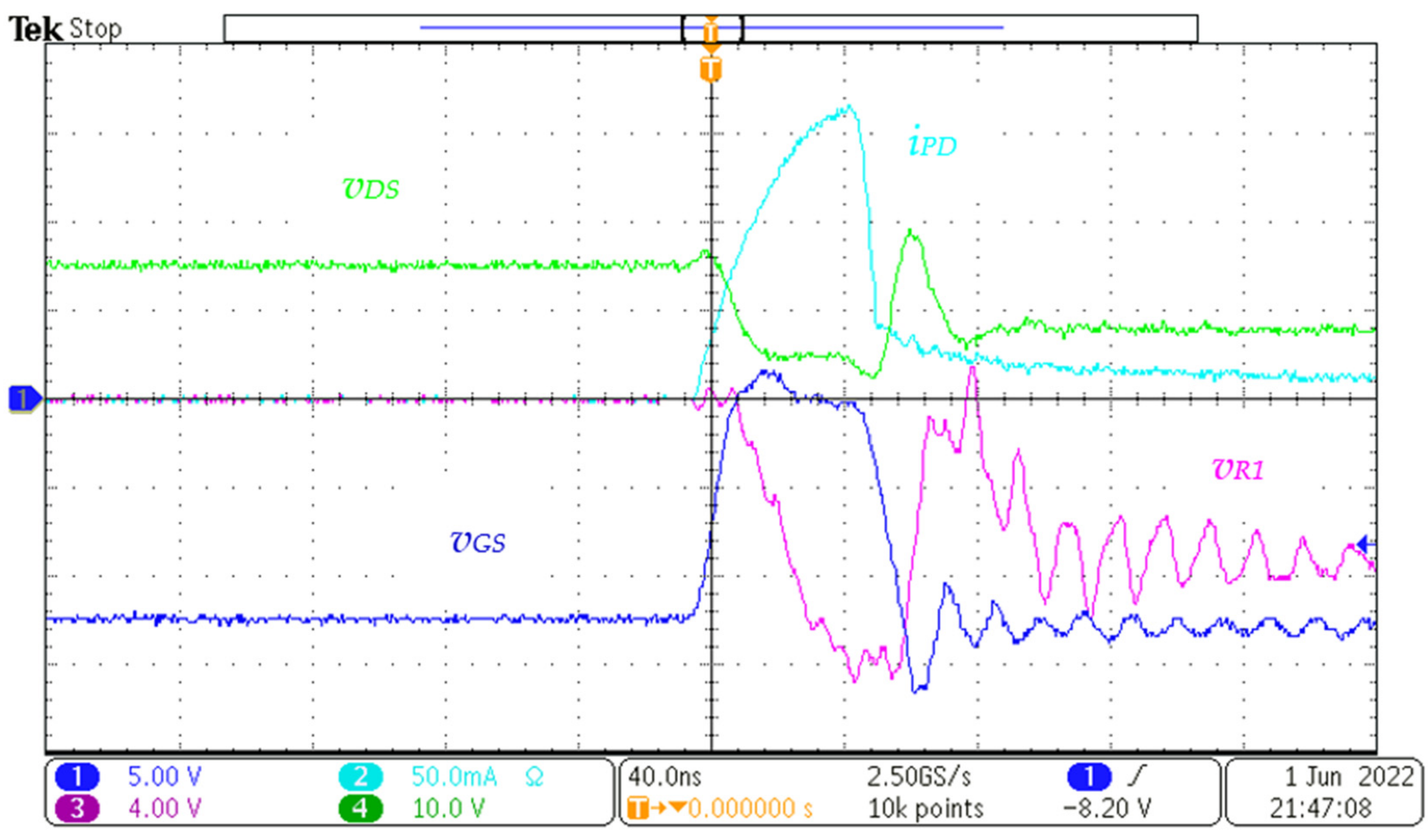
Figure 12. In
Figure 12, there are four curves. The first curve, in blue, is the gate-source voltage
vGS of the D-mode GaN HEMT. Because the D-mode GaN HEMT is a normally on device and the turn-on voltage of the D-mode GaN HEMT is −7 V, a charge pump gate drive is used, as shown in
Figure 6. The second curve, in green, is the drain-source voltage
vDS response of the D-mode GaN HEMT. We directly measured the
vDS using a difference voltage probe that has very low capacitance. The third curve, in purple, is the
vR1. As stated in
Section 3.4, the voltage response of
vR1 is similar to
vDS, with the only difference being in voltage shift. Comparing
vR1 in 4 V/div and
vDS in 10 V/div from the experimental result, we actually found the
vR1 is oscillating more than
vDS and with some amount of delay. The fourth curve, in cyan is the current taken from the photodetector, and the peak ampere is 165 mA. According to the power correcting factor calculated from 5 mm distance according to Equation (48) and the power conversion according to Equation (46), the peak power is calculated to be 81 W. It is also observed from
Figure 12 that there is still some amount of residual laser light showing on the photodetector, which may be due to the VCSEL resonance.
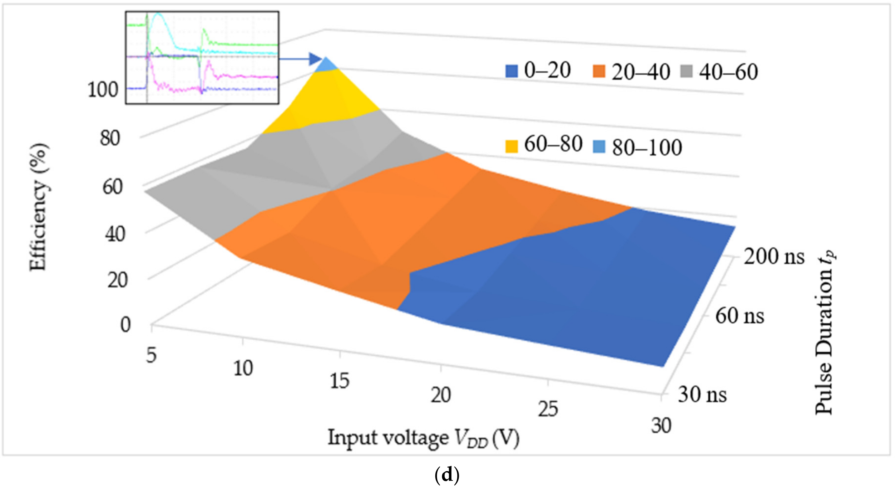
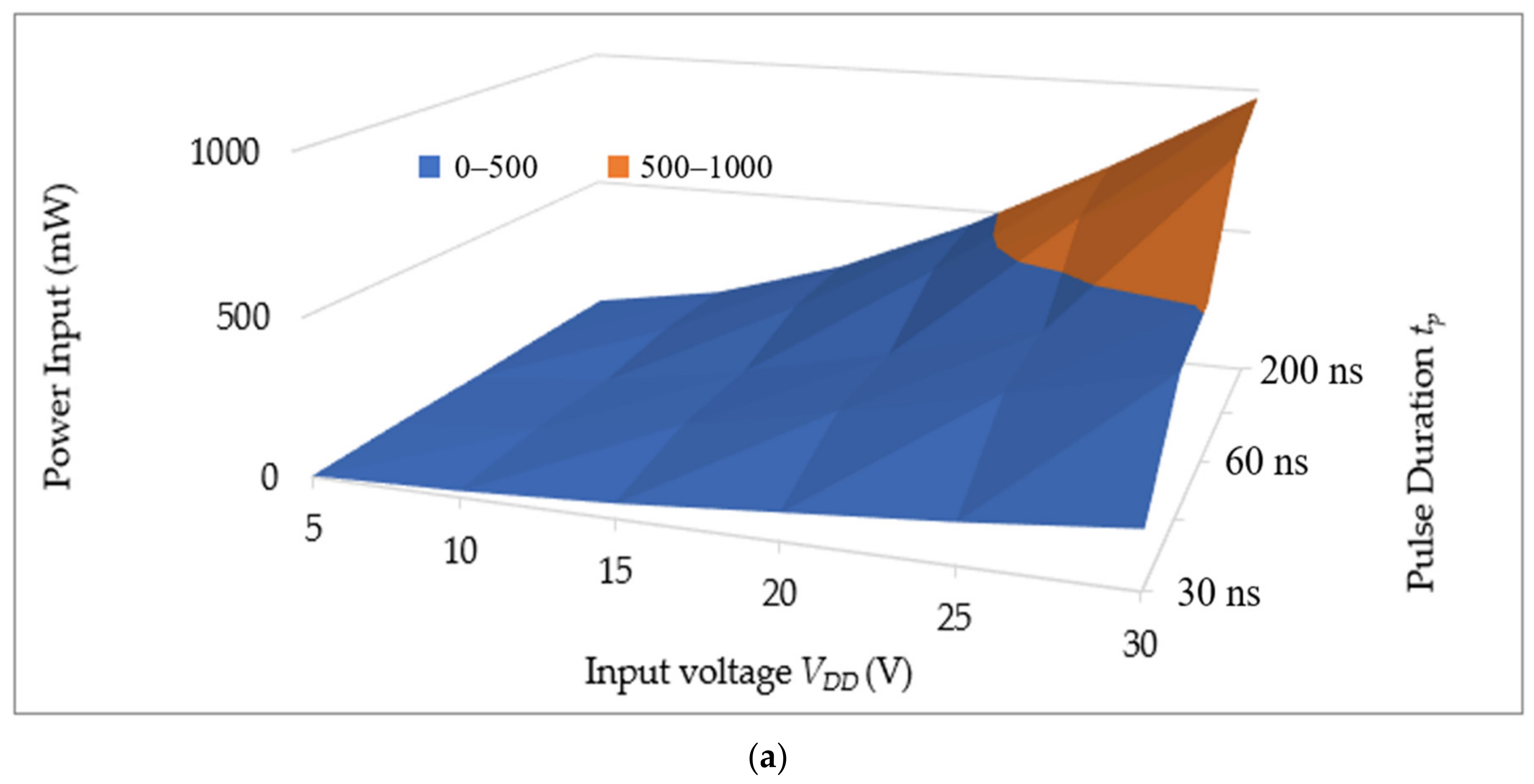
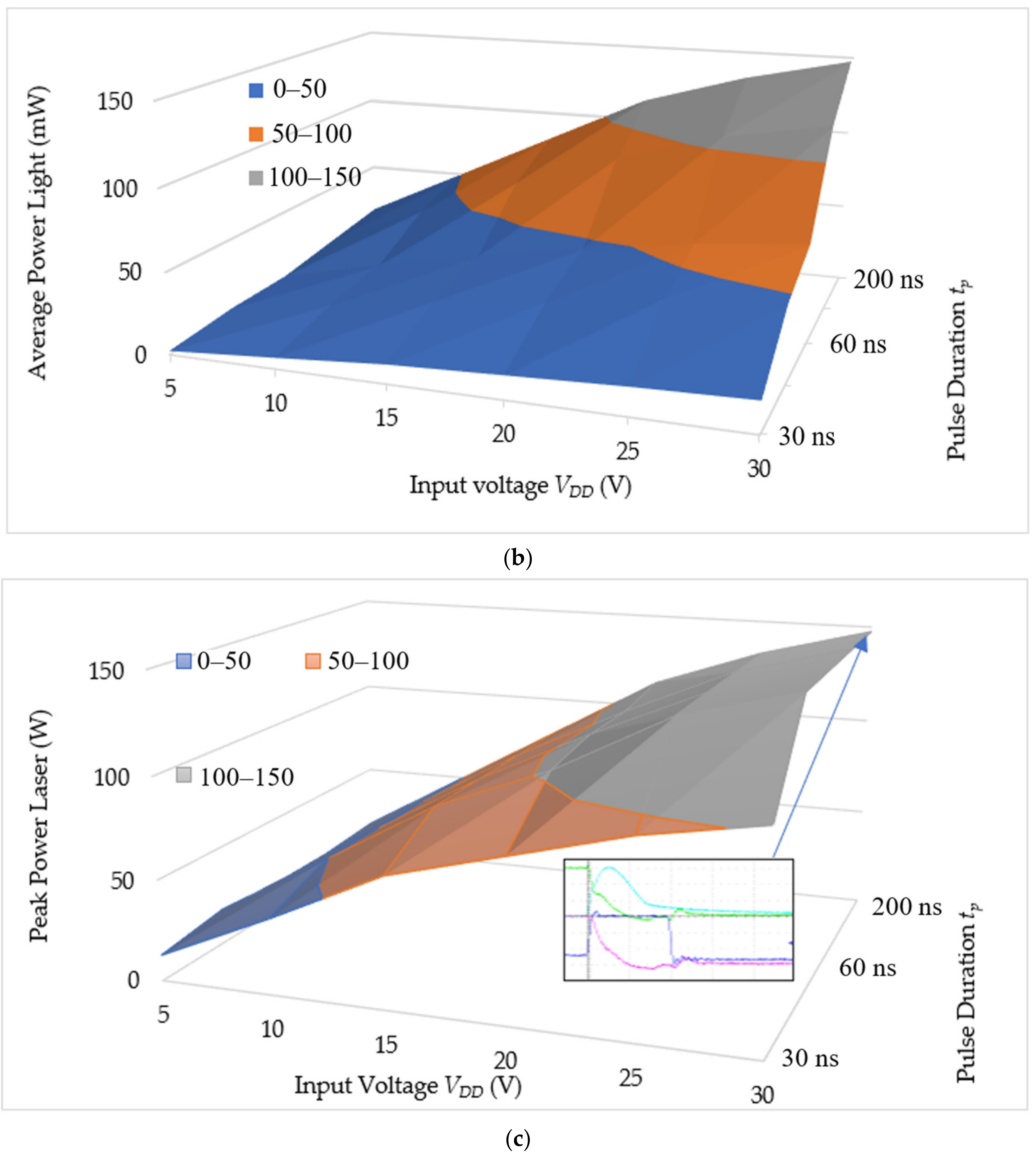
The performance measurement is summarized from many more experiments on the same experiment setup as shown in
Figure 11. The input power measured from the power supply reading is shown in
Figure 13a. The average lighting power is shown in
Figure 13b. The peak power shown in
Figure 13c is inconsistent with the power estimated in Equation (44): the higher the input voltage to the laser driver, the larger the peak power from the laser is. The efficiency from the electrical power input to the average laser output power is shown in
Figure 13d, which is inconsistent with Equation (40): the lower the input voltage, the higher the efficiency is. As a result, calculated from the experiments, we conclude that, for the current implementation, the highest efficiency is 86% and the maximum power is 150 W. Both the efficiency and the peak power stands for the turn-on time
ton, which should be no less than the pulse duration
tp,max. In
Figure 12, it is observed that when
ton is larger than
tp,max, the pulse duration remained at
tp,max = 100 ns when ignoring the residual light.
6. Discussion
When the VCSEL (around 30~40%) efficiency is unknown, the direct measurement, which imposed extra measurement inductance and capacitance on the VCSEL, is inappropriate for calculating the output power; therefore, we estimated the output power of a laser diode using the photodiode detector (PD) DET08CL. A standard method, such as the integrating sphere, collects electromagnetic radiation from a source completely external to the optical device and can be used to precisely measure the output power of the VCSEL laser. Other methods that split the optical beam into two branches [
23]—one is directed to an optical spectrum analyzer (OSA), and the other to the optical input of an oscilloscope—may also be used to measure the output power of the VCSEL laser. Although PD is not the best component for the absolute measurement mean, for the circuit designer it is simple and can provide enough relative information for the circuit designer to understand the relationships among the repetition rate, pulse duration, and the laser output power.
There are state-of-the-art commercial drivers for laser diode that can output higher repetition and short pulse duration, such as those from Analog Modules, Inc. (Longwood, Orlando, USA) Model 7612 A [
29] is capable of 1.25 W, 10 ns pulse width, and 50 MHz repetition rate. The driver circuit of this paper is oriented to yield a large instantaneous laser power output in an efficient way. The design specifications include a pulse duration of 10~100 ns and a 10 MHz repetition rate when the peak power is 100W. The high instantaneous laser power is due to our circuit design, as shown in
Figure 6. Our driver uses the D-mode GaN HEMT, which has a very small
Coss difference between turn-on and turn-off states, and which is used to drive the VCSEL made in NYCU. There are still areas for improvement, such as circuit fabrication, SiP (system in a package) IC design, and VCSEL efficiency, to be achieved in order to catch up with those state-of-the-art products.
The key factors of the output stability in the experiment include the stray inductance due to the wiring path of the laser diode (VCSEL in this study), the input parasitic capacitance Ciss of the GaN HEMT, and the cooling of the circuit board. Among these factors, the stray inductance is most critical factor. Extra stray inductance may result in reduction of the maximum output current and the maximum laser output power, which can be improved through shortening the current path from the laser to the capacitor C1 and to the transistor M1. Thus, flip-chip bonding instead of wire bonding is recommended for future work. The input parasitic capacitance is critical to achieve shorter pulse duration as well as higher repetition rate, which can be reduced by fabricating the GaN HEMT with a smaller gate width. A 20 mm GaN HEMT device will be introduced to replace the 120 mm device used in this paper, of which the differences between the devices and the laser output characteristics will be reported in future work. The copper pours, the clip bond, and the ribbon bond are solutions to enhance the heat dissipation of the laser diode driver circuit, which actually help the laser output stability.

 ,
, 

