Design of Compact, Broadband, and Low-Loss Silicon Waveguide Bends with Radius under 500 nm


Abstract
:1. Introduction
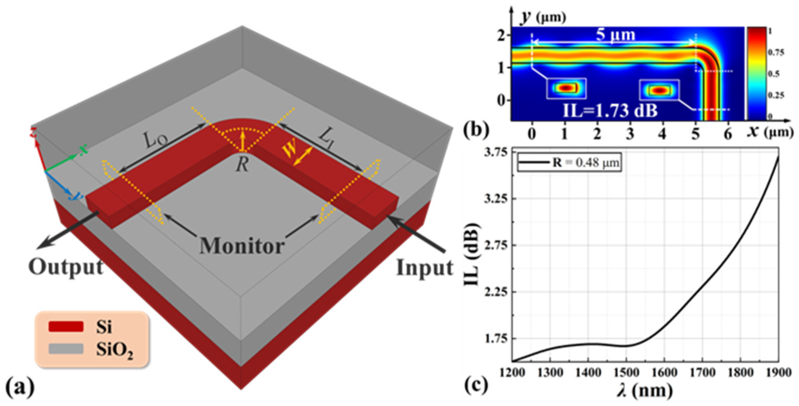
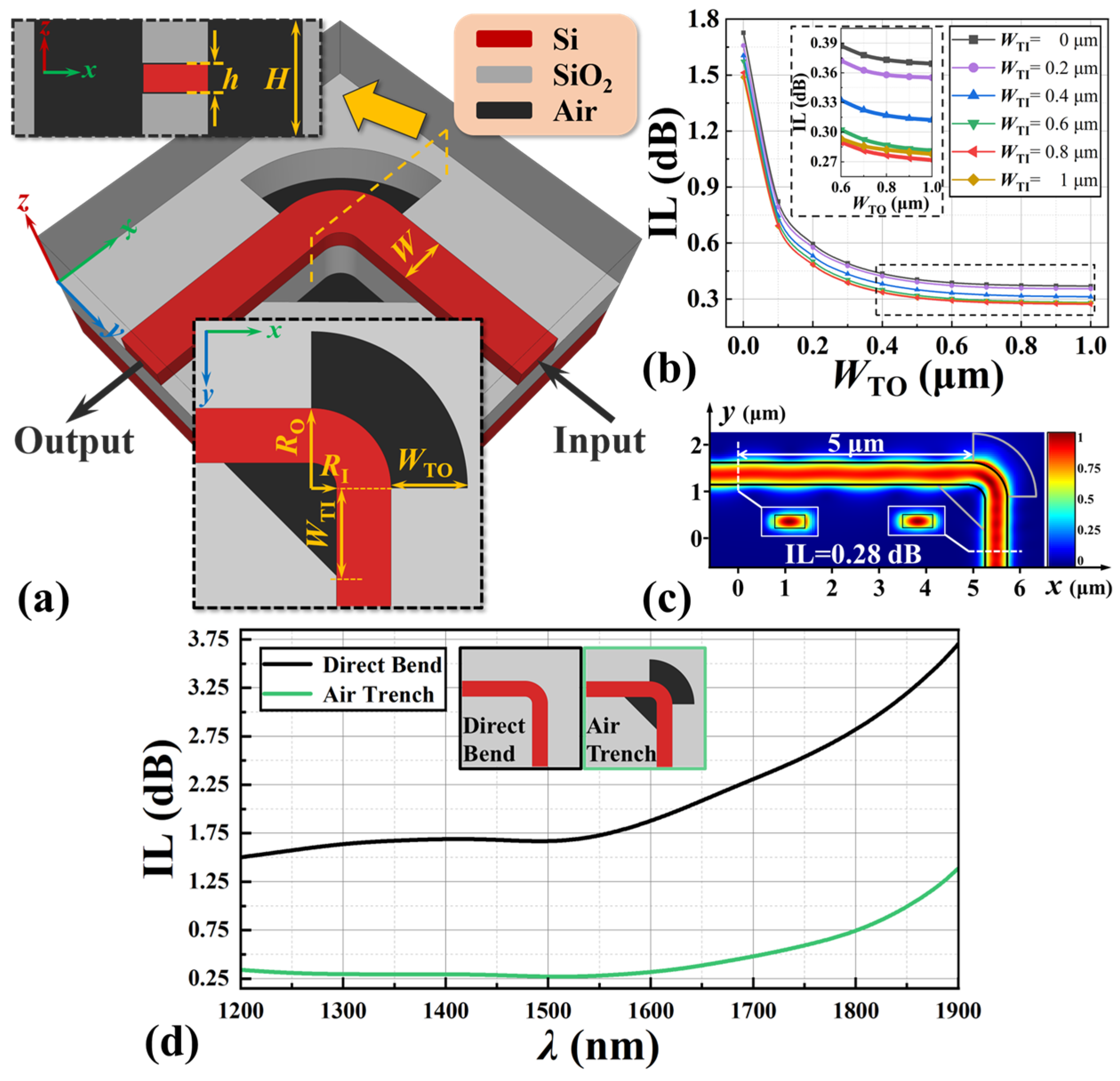
2. Device Structure and Principle
3. Results and Discussion
4. Conclusions
Author Contributions
Funding
Institutional Review Board Statement
Informed Consent Statement
Data Availability Statement
Conflicts of Interest
References
- Siew, S.Y.; Li, B.; Gao, F.; Zheng, H.Y.; Zhang, W.; Guo, P.; Xie, S.W.; Song, A.; Dong, B.; Luo, L.W.; et al. Review of silicon photonics technology and platform development. J. Light. Technol. 2021, 39, 4374–4389. [Google Scholar] [CrossRef]
- Margalit, N.; Xiang, C.; Bowers, S.M.; Bjorlin, A.; Blum, R.; Bowers, J.E. Perspective on the future of silicon photonics and electronics. Appl. Phys. Lett. 2021, 118, 220501. [Google Scholar] [CrossRef]
- Rahim, A.; Spuesens, T.; Baets, R.; Bogaerts, W. Open-access silicon photonics: Current status and emerging initiatives. Proc. IEEE 2018, 106, 2313–2330. [Google Scholar] [CrossRef]
- Smit, M.K.; Pennings, E.C.; Blok, H. A normalized approach to the design of low-loss optical waveguide bends. J. Light. Technol. 1993, 11, 1737–1742. [Google Scholar] [CrossRef]
- Neumann, E.-G.; Richter, W. Sharp bends with low losses in dielectric optical waveguides. Appl. Opt. 1983, 22, 1016–1022. [Google Scholar] [CrossRef] [PubMed]
- Jiang, X.; Wu, H.; Dai, D. Low-loss and low-crosstalk multimode waveguide bend on silicon. Opt. Express 2018, 26, 17680–17689. [Google Scholar] [CrossRef] [PubMed]
- Sun, T.; Xia, M. Low loss modified Bezier bend waveguide. Opt. Express 2022, 30, 10293–10305. [Google Scholar] [CrossRef]
- Sun, S.; Dong, P.; Zhang, F.; Wang, J.; Zhu, N.; Shi, Y. Inverse Design of Ultra-Compact Multimode Waveguide Bends Based on the Free-Form Curves. Laser Photonics Rev. 2021, 15, 2100162. [Google Scholar] [CrossRef]
- Kitoh, T.; Takato, N.; Yasu, M.; Kawachi, M. Bending loss reduction in silica-based waveguides by using lateral offsets. J. Light. Technol. 1995, 13, 555–562. [Google Scholar] [CrossRef]
- Cherchi, M.; Ylinen, S.; Harjanne, M.; Kapulainen, M.; Aalto, T. Dramatic size reduction of waveguide bends on a micron-scale silicon photonic platform. Opt. Express 2013, 21, 17814–17823. [Google Scholar] [CrossRef]
- Gao, S.; Wang, H.; Yi, X.; Qiu, C. Ultra-compact multimode waveguide bend with shallowly etched grooves. Opt. Express 2021, 29, 38683–38690. [Google Scholar] [CrossRef]
- Qian, Y.; Kim, S.; Song, J.; Nordin, G.P.; Jiang, J. Compact and low loss silicon-on-insulator rib waveguide 90° bend. Opt. Express 2006, 14, 6020–6028. [Google Scholar] [CrossRef]
- Lardenois, S.; Pascal, D.; Vivien, L.; Cassan, E.; Laval, S.; Orobtchouk, R.; Heitzmann, M.; Bouzaida, N.; Mollard, L. Low-loss submicrometer silicon-on-insulator rib waveguides and corner mirrors. Opt. Lett. 2003, 28, 1150–1152. [Google Scholar] [CrossRef]
- Xu, H.; Shi, Y. Ultra-sharp multi-mode waveguide bending assisted with metamaterial-based mode converters. Laser Photonics Rev. 2018, 12, 1700240. [Google Scholar] [CrossRef]
- Wu, H.; Li, C.; Song, L.; Tsang, H.K.; Bowers, J.E.; Dai, D. Ultra-sharp multimode waveguide bends with subwavelength gratings. Laser Photonics Rev. 2019, 13, 1800119. [Google Scholar] [CrossRef]
- Li, S.; Cai, L.; Gao, D.; Dong, J.; Hou, J.; Yang, C.; Chen, S.; Zhang, X. Compact and broadband multimode waveguide bend by shape-optimizing with transformation optics. Photonics Res. 2020, 8, 1843–1849. [Google Scholar] [CrossRef]
- Sun, C.; Yu, Y.; Chen, G.; Zhang, X. Ultra-compact bent multimode silicon waveguide with ultralow inter-mode crosstalk. Opt. Lett. 2017, 42, 3004–3007. [Google Scholar] [CrossRef]
- Song, J.H.; Kongnyuy, T.D.; De Heyn, P.; Lardenois, S.; Jansen, R.; Rottenberg, X. Low-loss waveguide bends by advanced shape for photonic integrated circuits. J. Light. Technol. 2020, 38, 3273–3279. [Google Scholar] [CrossRef]
- Lou, F.; Thylén, L.; Wosinski, L. Ultra-sharp bends based on hybrid plasmonic waveguides. In Proceedings of the 40th European Conference ECOC, Cannes, France, 9 September 2014; pp. 1–3. [Google Scholar] [CrossRef]
- Hu, T.; Qiu, H.; Zhang, Z.; Guo, X.; Liu, C.; Rouifed, M.S.; Littlejohns, C.G.; Reed, G.T.; Wang, H. A compact ultrabroadband polarization beam splitter utilizing a hybrid plasmonic Y-branch. IEEE Photonics J. 2016, 8, 4802209. [Google Scholar] [CrossRef]
- Banerji, S.; Majumder, A.; Hamrick, A.; Menon, R.; Sensale-Rodriguez, B. Ultra-compact integrated photonic devices enabled by machine learning and digital metamaterials. OSA Contin. 2021, 4, 602–607. [Google Scholar] [CrossRef]
- Banerji, S.; Majumder, A.; Hamrick, A.; Menon, R.; Sensale-Rodriguez, B. Machine learning enables design of on-chip integrated silicon T-junctions with footprint of 1.2 μm × 1.2 μm. Nano Commun. Netw. 2020, 25, 100312. [Google Scholar] [CrossRef]
- Shen, B.; Polson, R.; Menon, R. Metamaterial-waveguide bends with effective bend radius <λ0/2. Opt. Lett. 2015, 40, 5750–5753. [Google Scholar] [CrossRef]
- Liu, Y.; Sun, W.; Xie, H.; Zhang, N.; Xu, K.; Yao, Y.; Xiao, S.; Song, Q. Very sharp adiabatic bends based on an inverse design. Opt. Lett. 2018, 43, 2482–2485. [Google Scholar] [CrossRef]
- Molesky, S.; Lin, Z.; Piggott, A.Y.; Jin, W.; Vucković, J.; Rodriguez, A.W. Inverse design in nanophotonics. Nat. Photonics 2018, 12, 659–670. [Google Scholar] [CrossRef]
- Shang, Y.; Guo, W.; Wang, J.; Li, C.; Zhao, Y. Research of the bending loss of S-shaped waveguides with offsets and trenches. J. Mod. Opt. 2021, 68, 811–816. [Google Scholar] [CrossRef]
- Sullivan, D.M. Electromagnetic Simulation Using the FDTD Method; IEEE Press: Piscataway Township, NJ, USA, 2000. [Google Scholar]
- Lumerical FDTD Solutions. Available online: https://www.lumerical.com/products/fdtd/ (accessed on 16 April 2022).
- Palik, E.D. Handbook of Optical Constants of Solids; American Academic Press: Salt Lake City, UT, USA, 1998. [Google Scholar]
- Su, Y.; Zhang, Y.; Qiu, C.; Guo, X.; Sun, L. Silicon photonic platform for passive waveguide devices: Materials, fabrication, and applications. Adv. Mat. Technol. 2020, 5, 1901153. [Google Scholar] [CrossRef]
- Koester, S.J.; Schaub, J.D.; Dehlinger, G.; Chu, J.O. Germanium-on-SOI infrared detectors for integrated photonic applications. IEEE J. Sel. Top. Quantum Electron. 2006, 12, 1489–1502. [Google Scholar] [CrossRef]
- Ciminelli, C.; Innone, F.; Brunetti, G.; Conteduca, D.; Dell’Olio, F.; Tatoli, T.; Armenise, M.N. Rigorous model for the design of ultra-high Q-factor resonant cavities. In Proceedings of the 2016 18th International Conference on Transparent Optical Networks (ICTON), Tu.D6.3, Trento, Italy, 10–14 July 2016. [Google Scholar] [CrossRef]
- Liu, K.; Jin, N.; Cheng, H.; Chauhan, N.; Puckett, M.W.; Nelson, K.D.; Behunin, R.O.; Rakich, P.T.; Blumenthal, D.J. Ultralow 0.034 dB/m loss wafer-scale integrated photonics realizing 720 million Q and 380 μW threshold Brillouin lasing. Opt. Lett. 2022, 47, 1855–1858. [Google Scholar] [CrossRef]
- Manganelli, C.L.; Pintus, P.; Gambini, F.; Fowler, D.; Fournier, M.; Faralli, S.; Kopp, C.; Oton, C.J. Large-FSR thermally tunable double-ring filters for WDM applications in silicon photonics. IEEE Photonics J. 2017, 9, 6600310. [Google Scholar] [CrossRef]


| Reference | Structure | Bending Angle | Radius (μm) | Width (μm) | Footprint (μm2) | IL (dB) | BW (nm) |
|---|---|---|---|---|---|---|---|
| [18] [E] | BSO | 90° | 1 | 0.645 | 1.6 × 1.6 | 0.35 ± 0.05 | <100 (IL < 0.5 dB) |
| [19] [S] | SPP | 90° | 0.5 | 0.5 | ~1 × 1 | >1 | - |
| [21] [S] | ID | 180° | 0.38 | 0.44 | 1.2 × 1.2 | 1.73 | 25 (IL < 1.2 dB) |
| 90° | ~0.5 | 0.44 | 1.2 × 1.2 | 1.07 | 100 (IL < 2 dB) | ||
| [23] [E] | ID | 180° | 0.65 | 0.5 | 3 × 3 | 0.78 | 67 (IL < 1 dB) |
| This work [S] | AT | 90° | 0.48 | 0.5 | 2.2 × 2.2 | 0.28 | 500 (IL < 0.5 dB) |
| AT & Ge | 0.15 | 650 (IL < 0.5 dB) | |||||
| Ge Ⅰ/Ge Ⅱ | 0.12 | >650 (IL < 0.5 dB) |
Publisher’s Note: MDPI stays neutral with regard to jurisdictional claims in published maps and institutional affiliations. |
© 2022 by the authors. Licensee MDPI, Basel, Switzerland. This article is an open access article distributed under the terms and conditions of the Creative Commons Attribution (CC BY) license (https://creativecommons.org/licenses/by/4.0/).
Share and Cite
Zhang, Z.; Shi, Y.; Shao, B.; Zhou, T.; Luo, F.; Xu, Y. Design of Compact, Broadband, and Low-Loss Silicon Waveguide Bends with Radius under 500 nm. Photonics 2022, 9, 616. https://doi.org/10.3390/photonics9090616
Zhang Z, Shi Y, Shao B, Zhou T, Luo F, Xu Y. Design of Compact, Broadband, and Low-Loss Silicon Waveguide Bends with Radius under 500 nm. Photonics. 2022; 9(9):616. https://doi.org/10.3390/photonics9090616
Chicago/Turabian StyleZhang, Zhekang, Yuchen Shi, Bo Shao, Taotao Zhou, Fan Luo, and Yin Xu. 2022. "Design of Compact, Broadband, and Low-Loss Silicon Waveguide Bends with Radius under 500 nm" Photonics 9, no. 9: 616. https://doi.org/10.3390/photonics9090616
APA StyleZhang, Z., Shi, Y., Shao, B., Zhou, T., Luo, F., & Xu, Y. (2022). Design of Compact, Broadband, and Low-Loss Silicon Waveguide Bends with Radius under 500 nm. Photonics, 9(9), 616. https://doi.org/10.3390/photonics9090616