Abstract
We propose a multi-materials solar absorber consisting of regularly arranged cross resonators made of Ni, and nanocylinders made of Ti on their four corners. The finite difference time domain (FDTD) method is used to study the absorption performance of solar energy, the inherent absorption mechanisms and influencing factors of the absorber submerged in water. The proposed absorber achieves a nearly perfect absorption in the wavelength range of 300–2400 nm with an average absorptance higher than 98%, indicating that most of solar energy will be harvested. In addition, the high absorptance in the solar spectrum originates from the plasmon resonances of cross resonators and the magnetic polariton from the interaction between cross nanostructures and multi-material nanocylinders. Moreover, our absorbers are insensitive to the polarization of light due to the symmetry of the structures, but sensitive to the incident angle of the light. Most significantly, our absorbers can effectively prevent heat loss via radiation heat transfer by lowering their emissivity in the infrared region. The present study demonstrates a new design strategy for perfect solar absorbers consist of simple nanostructures made from multi-materials, which promise potential applications of solar energy harvesting and solar steam generation for desalination and wastewater treatment.
1. Introduction
Energy and environmental issues are attracting more and more attention [1,2]. It is expected that the world energy consumption will be increased by 48% from 2012 to 2040 [3], after which the greenhouse gases and atmospheric pollutants produced by the massive consumption of fossil fuels will also increase rapidly [4]. Thus, the development and utilization of renewable energy, such as energy from wind, water and solar, are being paid much attention by countries around the world due to their advantages of inexhaustibility and environmental protection. It is expected that by 2050, renewable energy will account for 63% of the total primary energy [5]. Among different renewable energies, solar energy shows great compatibility, whose utilization technologies are mainly divided into photothermal, photovoltaic, photosynthesis and photocatalysis [6,7,8,9], which are widely used in the fields of power generation, heating and disinfection [10]. However, traditional solar energy utilization methods are always limited by the low energy conversion efficiency [11]. Techniques that achieve the perfect absorption of solar energy have increasingly attracted the attention of researchers in the past decades [12].
The initial absorbing materials used for the solar absorber were mostly semiconductor [13], metal [14], oxide [15] and their mixtures [16]. Afterwards, the absorbing materials gradually developed into carbon materials [17] and polymers [18,19,20]. Then, with the development of nanomaterials, metamaterials began to be used for solar energy harvesting. The initial achievements of metamaterials were the theoretical discovery of the negative refractive index [21] and experimental verification [22], based on which, perfect lens [23], invisibility cloak [24] and other special applications have been achieved. Metamaterials exhibit the advantages of being able to stimulate plasmon resonances by adjusting their materials, structures and sizes, which can customize the absorption properties of the absorbers at the subwavelength scale [25,26,27]. Since the first metamaterial absorber was proposed by Landy in 2008 [12], more and more metamaterial absorbers for solar energy harvesting are being proposed [28,29,30]. The semiconductor, metal, oxide, and especially precious metals such as Pt, Au and Ag [31] were initially used. Natural hyperbolic materials such as Bi2Te3 and Bi2Se3 [32] and phase change materials such as VO2 [33] have also attracted widespread attention in recent years for their application for solar absorbers. Meanwhile, metamaterial absorbers composed of conical [34], square [35], spherical [36], humped [37], funnel-shaped [38], cruciform [39] and cylindrical [40] arrays have been continuously proposed.
Based on metamaterials with different structures and materials, numerous solar absorbers have been proposed in the past 10 years [41]. For nanostructures made of only one material, a metamaterial absorber based on an amorphous silicon nanocone array from Zhu et al. [34] maintained an absorptance of above 93% in the wavelength range of 400–650 nm. A self-assembled plasmonic absorber proposed by Zhou et al. [42] achieved almost perfect absorption of light in the wavelength range of 400 nm to 10 mm. For nanostructures made of multiple materials in the vertical direction, Qin et al. [43] proposed a metamaterial absorber based on SiO2–TiN–SiO2 of layered nanodisk arrays, achieving an absorptance of 99% in the wavelength range of 645–2290 nm. We also proposed solar absorbers with different nanostructures made of different materials, achieving nearly 100% solar energy harvesting [44,45]. It is clear that metamaterial absorbers with nanostructures made from multiple materials exhibit more merits for solar energy harvesting.
However, a perfect solar absorber should not only totally absorb the incident solar energy, but also dissipate as little energy as possible via radiation heat transfer. Based on the merits of metamaterials made from multiple materials, a typical three-layer multi-materials solar absorber is proposed in the present study. The absorption characteristics and influencing factors of the proposed absorber are studied by using the finite difference time domain (FDTD) method, and the underlying mechanisms are also numerically revealed by employing the electric field distributions and current vectors. The nearly total absorption of solar energy originates from the stimulus of both electric polaritons and magnetic polaritons because of the interaction between different morphological nanostructures and multiple materials for them. Most significantly, our absorbers exhibit extremely low emissivity in the infrared region, where the emissive light of a surface with a temperature around 100 °C is located. The extremely low emissivity of our absorbers will greatly suppress their radiation heat transfer, ultimately enhancing their total solar energy utilization efficiency. When submerged in water, our solar absorbers promise applications of solar steam generation with super-high solar energy conversion efficiency, such as sewage purification, seawater desalination, and so on.
2. Model and Methods
The incident light is absorbed (A), reflected (R) and transmitted (T) by an object, so the absorptance of a surface can be obtained based on the reflectance and transmittance with A = 1–T–R. Thus, reducing the reflectance and transmittance of an absorber is the key point to enhance its absorptance. In the present study, the proposed absorber consists of cross nanostructures on the top with four nanocylinders on their four corners (Figure 1). In addition, there is a Al2O3 dielectric layer in-between with a Ag reflection layer at the bottom, and a Si substrate to support the whole structure. Moreover, a thin SiO2 layer is covered on the top of the nanostructures to reduce the reflectance because of the impedance matching effect.
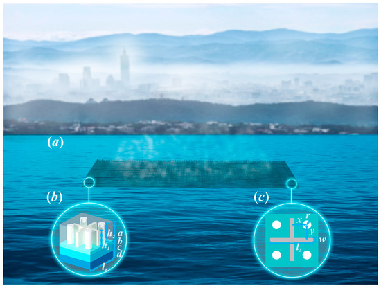
Figure 1.
The schematic of the proposed absorber. (a) Three–dimensional schematic of the absorber. (b) The sectional view of a single unit. (c) The top view of a single unit of the absorber.
A unit cell is shown in Figure 1b with its top view demonstrated in Figure 1c, respectively. The geometric parameters of the structure are represented by the following symbols: the thickness of the top SiO2 layer, Al2O3 dielectric layer, Ag reflective layer and Si substrate are represented by a, b, c and d, respectively. In addition, the periodicity of the unit is l1 in both the x and y directions. The height, length and width of the cross nanostructures on the top are indicated by h1, l2 and w, respectively. Moreover, the height and radius of the nanocylinder are respectively h2 and r, and the distances from the horizontal and vertical coordinates to the center of the four nanocylinders are represented by x and y, respectively. The optimized values of those parameters are as follows: a = 245 nm; b = 20 nm; c = 100 nm; d = 300 nm; l1 = 240 nm; l2 = 206 nm; h1 = 160 nm; h2 = 220 nm; w = 20 nm; r = 25 nm; and x = y = 75 nm. These parameters are set as default unless otherwise declared.
The FDTD method based on Maxwell’s equations is used to calculate the absorption properties of our absorbers. The periodic boundary conditions are used in both x and y directions according to the periodicity of the nanostructures, while the boundary condition in the z direction is set as the perfect matched layer (PML). As for the materials used in the present study, the dielectric functions of Ti, Ni and Ag are obtained from CRC [46], the dielectric functions of SiO2, Al2O3, Si and Pt are taken from the data compiled by Palik [47], and the dielectric functions of Bi2Te3 and graphite are taken from Esslinger [48] and M. R. Querry [49], respectively. In addition, the surrounding medium of the proposed absorber is water with a refractive index of 1.33 in the interested spectrum, with the purpose of potential applications of our proposed absorber for solar vapor generation.
3. Results and Discussion
3.1. Nearly Perfect Absorption of Our Absorber for Solar Energy Harvesting
The absorption properties of the proposed absorber with default parameters in the wavelength range of 300–2400 nm are depicted in Figure 2. It can be clearly seen that the absorber achieves an absorptance of over 94% throughout the solar spectrum. Specifically, there are absorption peaks of nearly 100% at wavelengths around 340, 585, 1160, and 2160 nm. In addition, the absorptance of the proposed absorber is higher than 96.5% in the whole wavelength range from 320 nm to 2400 nm with an average absorptance higher than 98%, indicating that the proposed absorber achieves a nearly perfect solar energy absorption. The transmittance of our absorber is 0 because of the opaque Ag layer at the bottom, and the reflectance of our absorber is also near to 0. Furthermore, there are multiple absorption peaks on the absorption spectrum of the proposed absorber.
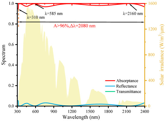
Figure 2.
The absorption properties of the proposed absorber. The red, blue and green lines represent the absorptance, reflectance and transmittance of the absorber in the wavelength range of 300–2400 nm, respectively.
3.2. Underlying Mechanisms of the Perfect Absorption of Solar Energy
To further reveal the underlying mechanisms of the nearly perfect solar absorption of our absorber, we analyze the electric fields of the absorber at different wavelengths (Figure 3). The electric fields inside the absorber at λ = 310 nm (the lowest absorptance), 585 nm and 2160 nm (the highest absorptance) are plotted. Figure 3a–c show the electric fields of the absorber in the plane of y = 0, while Figure 3d–f show the electric fields of the absorber in the plane of y = 75 nm, respectively. It can be seen that the high electric field intensity generally distributes at the upper and sidewalls of the nanostructures, indicating that there are strong electric plasmon resonances on the surface of the nanostructures. However, the magnitude of the plasmon resonances at different wavelengths varies with each other, leading to the slight difference of the absorptance of the absorber. Moreover, there is strong plasmon resonance in the zone coexistence of both the cross nanostructures and nanocylinders, demonstrating that the interaction between those two kinds of nanostructures further enhances the absorptance of the absorber.
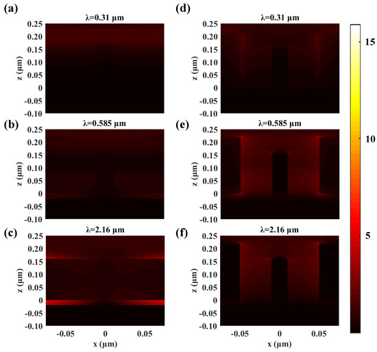
Figure 3.
Electric field distribution of the absorber at different wavelengths. (a–c) The electric field distributions of the absorber in the plane of y = 0 at three wavelengths of 310, 585 and 2160 nm, respectively. (d–f) The electric field distributions of the absorber in the plane of y = 75 nm at three wavelengths of 310, 585 and 2160 nm, respectively.
In addition, the current vector distributions of the absorber in x–z plane and x–y plane at λ = 2160 nm are drawn (Figure 4a–d) to further clarify the interaction between cross nanostructures and nanocylinders. Figure 4a shows the current vector distribution in the x–z plane at y = 0. It can be seen that there is a clockwise current vector cycle in the upper, while there are two anticlockwise current vector cycles at the middle and bottom of the nanostructures, and the three current vector cycles indicate the existence of magnetic polaritons. Moreover, the current vector distributions in the x–y plane at z = 80 nm and 160 nm at the wavelength of 2160 nm are respectively shown in Figure 4c,d. It can be seen from Figure 4c that current vector cycles appear in the upper and lower middle regions in the opposite directions, indicating there is strong magnetic dipole resonance, while there are no current vector distributions at z = 160 nm (Figure 4d). The results clearly demonstrate that the coexistence of cross nanostructures and nanocylinders arouse strong magnetic polaritons inside the proposed absorber, which greatly enhances its absorptance.
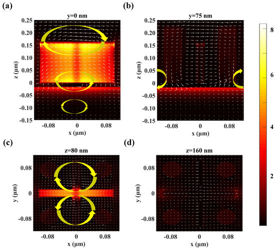
Figure 4.
Current vector distributions of the absorber at the wavelength of 2160 nm. (a,b) The current vector distribution in the x–z plane at y = 0 and 75 nm, respectively. (c,d) The current vector distribution in the x–y plane at z = 80 and 160 nm, respectively.
The power dissipation density inside the absorber can be calculated by the following formula [32]:
where ε0 is the vacuum permittivity, ε″ is the imaginary part of the dielectric function of the materials and |E| is the magnitude of the electric field. The power dissipation density distributions are inside the absorber in the x–z plane at y = 0 and y = 75 nm when λ = 2160 nm are additionally presented in Figure 5. In order to make the results more distinct, the values in the figures are taken as the logarithm of the original values (log 10). It can be seen that the energy of the incident light mainly dissipates inside the nanostructures, with the strongest section appearing on the surface of the nanostructures. Moreover, there a small amount of energy dissipates inside the Ag substrate. Furthermore, Figure 5b shows the power dissipation density in the x–z plane at y = 75 nm, in which the data are also the logarithm of the original values (log 10). The results in Figure 5b clearly reveal that more energy is dissipated inside the nanocylinders instead of the cross nanostructures, demonstrating that the nanocylinders also play a key role in the total absorption of incident light.
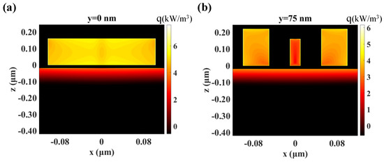
Figure 5.
Power dissipation density distributions inside the absorber. (a) The power dissipation density in x–z plane at y = 0. (b) The power dissipation density in x–z plane at y = 75 nm. The wavelength is 2160 nm and the values of the power dissipation distributions in the figures are taken as the logarithm of the original values (log 10).
3.3. Emission Suppression in Mid–Infrared Region of the Absorber
We further extend the calculation to a wavelength range of 0.3–12 μm to explore the emissivity of our absorbers in the infrared region. As demonstrated in Figure 6, our absorber presents a high solar energy harvesting efficiency, but the absorptance of the absorber drastically decreases to an extremely low level when λ > 2500 nm. According to Kirchhoff’s law of thermal radiation, the absorptance of an object is identical to the emissivity at the same temperature under the condition of thermal equilibrium. It means that our absorber can radiate as little energy as possible in the band where there is no solar radiation energy, and “lock” the absorbed solar energy inside the absorber. The spectral emissive power of a blackbody with different temperatures is also shown in Figure 6. It should be noted that the temperature of our absorber does not exceed 200 ℃ as it is only irradiated by one sun. The average emissivity of our absorbers at the temperatures of 293.15 K, 323.15 K, 353.15 K, 383.15 K, 413.15 K, 443.15 K and 473.15 K is 5.34%, 5.35%, 5.46%, 5.70%, 6.09%, 6.63% and 7.33%, respectively. The results clearly demonstrate that our absorber only radiates very little energy in the infrared region. Figure 2 and Figure 6 show that our proposed absorber can not only capture solar radiation energy effectively, but also prevent dissipation of the energy via radiation heat transfer.
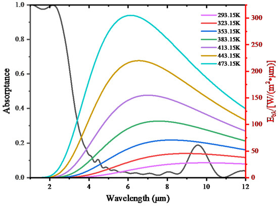
Figure 6.
The absorption spectrum of the absorber in part of the infrared region and the spectral emissive power of a blackbody varies with temperatures.
3.4. Effects of Materials on Absorptance of the Absorber
The influences of materials on the absorption properties of our absorbers are further analyzed. We used five different material combinations for the cross nanostructures and the nanocylinders in this section, which are metal and nonmetal, nonmetal and nonmetal, metal and metal, single metal, metal and precious metal, respectively. The results are shown in Figure 7, from which we can see that the absorption properties of the absorbers made from different material combinations are totally different. The absorber presents the highest absorptance when Ni and Ti are respectively selected as the materials for cross nanostructures and nanocylinders. Comparing nanostructures made of Ni–Ni with Ni–Ti, it is noted that the absorptance of the former is poor to the latter in the visible band, but it exhibits a similar performance in the remaining bands, indicating that cross nanostructures and nanocylinders made from different materials also contribute to solar energy harvesting.
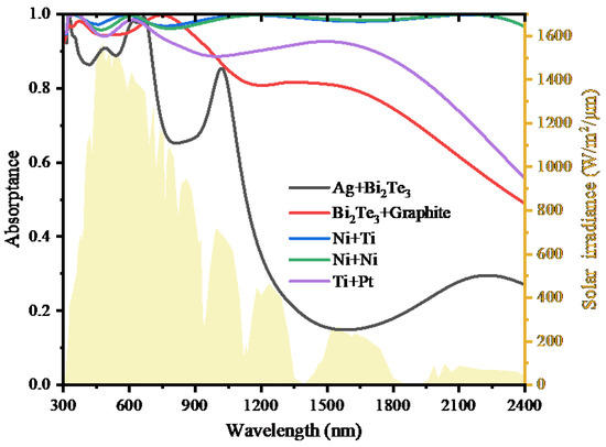
Figure 7.
The absorption spectra of the absorbers with different materials.
3.5. Effects of Geometric Parameters on the Absorption Properties of the Absorbers
The influences of geometric parameters on the absorption properties of the absorber are numerically studied. The results are shown in Figure 8, from which a solar absorber with the best absorption characteristics in the wavelength range of 300–2400 nm is obtained by optimizing the geometric parameters. First, the role of the Ag layer is to reflect transmitted light back into the nanostructures to be reabsorbed. When the thickness of Ag is 100 nm, the proposed absorber has the best absorption properties (Figure 8a), and the absorption properties cannot be further optimized by increasing the thickness of the Ag layer. However, a thin Ag layer (c = 50 nm) lowers the absorptance of the absorber, and a suitable Ag layer can be calculated by with d as the penetration depth of a surface and κ representing the extinction coefficient of the material at the wavelength of λ.
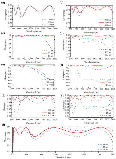
Figure 8.
The absorption spectra of the proposed absorbers with different geometric parameters. (a) The thickness of the Ag layer. (b) The thickness of the SiO2 layer. (c) The thickness of the Al2O3 layer. (d) The height of the cross structure. (e) The length of the cross nanostructures. (f) The width of the cross nanostructures. (g) The height of the nano-cylinders. (h) The radius of the nano-cylinders. (i) The coordinate distances (x and y) between the bottom center of the nano-cylinders and the x and y axes.
Figure 8b shows the influence of the thickness of the SiO2 layer (a) on the absorption spectra of the absorbers. By comparing the absorption properties of the absorbers with a = 200, 245 and 400 nm, it can be seen that an absorber exhibits the highest absorptance in the solar spectrum when a = 245 nm. A thicker SiO2 layer increases the absorptance of the absorber in the bands of 800–1140 nm and 1320–2120 nm but reduces it in the range of 590–790 nm. On the contrary, a thinner SiO2 layer increases the absorptance of the absorber in the range of 470–570 nm but reduces the it in the regions of 320–460 and 580–2400 nm. Moreover, the influence of the thickness of the Al2O3 layer (b) on the absorption spectra of the absorbers is shown in Figure 8c. The absorber presents the best absorption properties when b = 20 nm. A thicker Al2O3 layer increases the absorptance of the absorber in the bands of 635–910 nm but reduces it in the bands of 920–2280 nm. In contrast, a thinner Al2O3 layer enhances the absorptance of absorbers in the wavelength range of 1230–1680 nm but reduces it in the range of 1690–2400 nm.
Figure 8d shows the influence of cross nanostructures’ height on the absorptance of the absorber. An absorber presents the highest absorptance when h1 = 160 nm. Both higher and lower cross nanostructures reduce its absorptance in almost all bands. In addition, the length of cross nanostructures makes a big difference on the absorption spectrum of the absorber (Figure 8e). An absorber has the highest absorptance when l2 = 206 nm. Both longer and shorter cross nanostructures reduce the absorptance of absorber in almost all bands. Furthermore, the width of cross nanostructures also influences the absorptance of absorbers (Figure 8f). An absorber has the highest absorptance when w = 20 nm. Wider cross nanostructures increase the absorptance of absorbers in the regions of 350–880 nm and reduce it at 890–2400 nm. In contrast, narrower cross nanostructures reduce the absorptance of absorbers in almost all bands.
The effects of geometric parameters of nanocylinders on the absorption properties of the absorber are shown in Figure 8g,h. It can be seen that the proposed absorber exhibits the best absorption properties when h2 = 220 nm (Figure 8g). Higher nanocylinders increase the absorptance of the absorber in the bands of 780–1020 and 1430–2050 nm. Meanwhile, the absorptance in the bands of 600–770, 1030–1420 and 2060–2400 nm is reduced. In contrast, lower nanocylinders increase the absorptance of absorbers at 730–990 nm but reduce it at 320–720 and 1000–2400 nm. Furthermore, an absorber has the best absorption properties when r = 25 nm (Figure 8h). Larger nanocylinders reduce the absorptance of the absorber in almost all bands. In contrast, smaller nanocylinders improve the absorptance at 660–990 nm but reduce it at 320–650 nm and 1000–2400 nm.
Figure 8i shows the effect of the coordinate distances between the bottom center of the nanocylinders and the x and y axes (x and y) on the absorptance of the proposed absorbers. The best absorption performance is obtained when both x and y are 75 nm. A larger x and y improves the absorptance at 380–540 nm, 700–830 nm and 2180–2400 nm, but reduces it at 550–690 nm and 840–2170 nm. In contrast, a smaller x and y improves the absorptance of absorbers in the ranges of 1150–1950 nm but reduces it in the regions of 550–1140 nm and 1970–2400 nm.
3.6. Polarization Independence of the Absorber
To further evaluate the absorption performance of the absorber, the effects of polarization of the light on the absorption properties of our absorbers are additionally analyzed. The morphology and geometric parameters of the absorber are set as default, the polarization angle of the incident light varies in the range of 0–90° at an interval of 1°, and the results are presented in Figure 9a. It can be seen that the absorptance of the absorber is similar with the polarization angle of the incident light varying in the range of 0–90°, showing the polarization independence of our absorbers because of its tetrahedral symmetrical nanostructures. However, the incident angle of the light makes a big difference on the absorption properties of the absorber. The absorptance of the absorber increases with the increase of the incident angle before reaching the maximum with an incident angle of 40°, and then the absorptance of the absorber decreases with the further increase of the incident angle (Figure 9b). The reason for such a result is the interaction effect of the different materials of the nanostructures and their different morphologies, which generates numerous electric polaritons and magnetic polaritons (Figure 10).
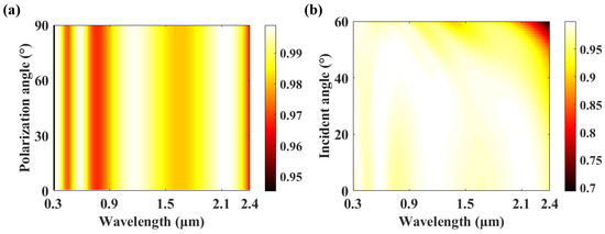
Figure 9.
The absorption spectra of the default absorber with the polarization angle varying in the range of 0–90° and the incident angle varying in the range of 0–60°. (a) The dependence of absorption properties of the absorber on the polarization of the light. (b) The effects of incident angles of the light on the absorption properties of the proposed absorber.
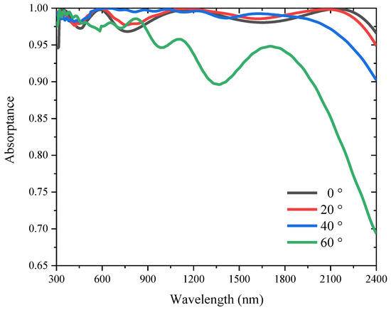
Figure 10.
The absorption spectra of the default absorber with different incident angles.
4. Conclusions
In summary, we propose a polarization–independent absorber, which consists of regularly arranged Ni cross nanostructures and Ti nanocylinders. By adopting a metal–insulator–metal multilayer structure, numerous plasmon resonances between structures and materials are stimulated. The absorber achieves over 96% absorptance in the wavelength range of 320–2400 nm with an average absorptance of more than 98% in the interested wavelength range, indicating a near perfect absorption of solar energy. In addition, the geometric parameters of the absorber make a difference on its absorption properties with a small tolerance. Most significantly, the proposed absorber has extremely low emissivity in the infrared region, which drastically lowers the radiation heat transfer for a surface with a temperature lower than 200 °C. The present study paves the way for a new design strategy of absorbers with high solar energy harvesting efficiency, but extremely low emissivity in the infrared region, to achieve high solar energy utilization and promise applications for solar steam generation.
Author Contributions
Conceptualization, methodology and funding acquisition, and supervision, Z.W.; software, data curation and writing—original draft preparation, Y.W.; validation, writing—review and editing Z.L., G.D., D.Y. and P.C. All authors have read and agreed to the published version of the manuscript.
Funding
This work was supported by the National Natural Science Foundation of China through Grant No. 52006056, Natural Science Foundation of Hunan through Grant No. 2020JJ3012, and the Experiments for Space Exploration Program and the Qian Xuesen Laboratory, China Academy of Space Technology (Grant No. TKTSPY–2020–01–04).
Institutional Review Board Statement
Not applicable.
Informed Consent Statement
Not applicable.
Conflicts of Interest
The authors declare no conflict of interest.
References
- Romero, M.; Steinfeld, A. Concentrating solar thermal power and thermochemical fuels. Energy Environ. Sci. 2012, 5, 9234–9245. [Google Scholar] [CrossRef]
- Eliasson, J. The rising pressure of global water shortages. Nature 2015, 517, 6. [Google Scholar] [CrossRef]
- Conti, J.; Holtberg, P.; Diefenderfer, J.; LaRose, A.; Turnure, J.T.; Westfall, L. International Energy Outlook 2016 with Projections to 2040; Office of Energy Analysis: Washington, DC, USA, 2016. [Google Scholar]
- Montzka, S.A.; Dlugokencky, E.J.; Butler, J.H. Non–CO2 greenhouse gases and climate change. Nature 2011, 476, 43–50. [Google Scholar] [CrossRef] [PubMed]
- Gielen, D.; Boshell, F.; Saygin, D.; Bazilian, M.D.; Wagner, N.; Gorini, R. The role of renewable energy in the global energy transformation. Energy Strateg. Rev. 2019, 24, 38–50. [Google Scholar] [CrossRef]
- Wang, Z.; Quan, X.; Yao, W.; Wang, L.; Cheng, P. Plasma resonance effects on bubble nucleation in flow boiling of a nanofluid irradiated by a pulsed laser beam. Int. Commun. Heat Mass Transfer 2016, 72, 90–94. [Google Scholar] [CrossRef]
- Wang, Z.; Zhang, Z.M.; Cheng, P. Natural anisotropic nanoparticles with a broad absorption spectrum for solar energy harvesting. Int. Commun. Heat Mass Transfer 2018, 96, 109–113. [Google Scholar] [CrossRef]
- Wang, Z.; Zhang, Z.M.; Quan, X.; Cheng, P. A numerical study on effects of surrounding medium, material, and geometry of nanoparticles on solar absorption efficiencies. Int. J. Heat Mass Transfer 2018, 116, 825–832. [Google Scholar] [CrossRef]
- Wang, Z.; Yang, P.; Qi, G.; Zhang, Z.M.; Cheng, P. An experimental study of a nearly perfect absorber made from a natural hyperbolic material for harvesting solar energy. J. Appl. Phys. 2020, 127, 233102. [Google Scholar] [CrossRef]
- Elimelech, M.; Phillip, W.A. The future of seawater desalination: Energy, technology, and the environment. Science 2011, 333, 712–717. [Google Scholar] [CrossRef]
- Aman, M.M.; Solangi, K.H.; Hossain, M.S.; Badarudin, A.; Jasmon, G.B.; Mokhlis, H.; Bakar, A.H.A.; Kazi, S.N. A review of safety, health and environmental (SHE) issues of solar energy system. Renew. Sustain. Energ. Rev. 2015, 41, 1190–1204. [Google Scholar] [CrossRef]
- Landy, N.I.; Sajuyigbe, S.; Mock, J.J.; Smith, D.R.; Padilla, W.J. Perfect metamaterial absorber. Phys. Rev. Lett. 2008, 100, 207402. [Google Scholar] [CrossRef] [PubMed]
- Gittleman, J.I.; Sichel, E.K.; Lehmann, H.W.; Widmer, R. Textured silicon: A selective absorber for solar thermal conversion. Appl. Phys. Lett. 1979, 35, 742–744. [Google Scholar] [CrossRef]
- Liang, Q.; Yin, Q.; Chen, L.; Wang, Z.; Chen, X. Perfect spectrally selective solar absorber with dielectric filled fishnet tungsten grating for solar energy harvesting. Sol. Energy Mater. Sol. Cells 2020, 215, 110664. [Google Scholar] [CrossRef]
- Barrera, E.; González, I.; Viveros, T. A new cobalt oxide electrodeposit bath for solar absorbers. Sol. Energy Mater. Sol. Cells 1998, 51, 69–82. [Google Scholar] [CrossRef]
- Farooq, M.; Green, A.A.; Hutchins, M.G. High performance sputtered Ni:SiO2 composite solar absorber surfaces. Sol. Energy Mater. Sol. Cells 1998, 54, 67–73. [Google Scholar] [CrossRef]
- Wang, Z.; Quan, X.; Zhang, Z.; Cheng, P. Optical absorption of carbon–gold core–shell nanoparticles. J. Quant. Spectrosc. Radiat. Transfer 2018, 205, 291–298. [Google Scholar] [CrossRef]
- Chen, L.; Duan, G.; Zhang, C.; Cheng, P.; Wang, Z. 3D printed hydrogel for soft thermo–responsive smart window. Int. J. Extreme Manuf. 2022, 4, 025302. [Google Scholar] [CrossRef]
- Zhan, Z.; Chen, L.; Duan, H.; Chen, Y.; He, M.; Wang, Z. 3D printed ultra–fast photothermal responsive shape memory hydrogel for microrobots. Int. J. Extreme Manuf. 2021, 4, 015302. [Google Scholar] [CrossRef]
- Wang, Z.; Zhan, Z.; Chen, L.; Duan, G.; Cheng, P.; Kong, H.; Chen, Y.; Duan, H. 3D–printed bionic solar evaporator. Sol. RRL 2022, 6, 2101063. [Google Scholar] [CrossRef]
- Veselago, V.G. Reviews of topical problems: The electrodynamics of substances with simultaneously negative values of\epsilon and μ. Sov. Phys. Usp. 1968, 10, R04. [Google Scholar] [CrossRef]
- Shelby, R.A.; Smith, D.R.; Schultz, S. Experimental verification of a negative index of refraction. Science 2001, 292, 77–79. [Google Scholar] [CrossRef] [PubMed]
- Fang, N.; Lee, H.; Sun, C.; Zhang, X. Sub–diffraction–limited optical imaging with a silver superlens. Science 2005, 308, 534–537. [Google Scholar] [CrossRef] [PubMed]
- Schurig, D.; Mock, J.J.; Justice, B.J.; Cummer, S.A.; Pendry, J.B.; Starr, A.F.; Smith, D.R. Metamaterial electromagnetic cloak at microwave frequencies. Science 2006, 314, 977–980. [Google Scholar] [CrossRef]
- Chen, H.; Chan, C.T.; Sheng, P. Transformation optics and metamaterials. Nat. Mater. 2010, 9, 387–396. [Google Scholar] [CrossRef] [PubMed]
- Liang, Y.; Koshelev, K.; Zhang, F.; Lin, H.; Lin, S.; Wu, J.; Jia, B.; Kivshar, Y. Bound states in the continuum in anisotropic plasmonic metasurfaces. Nano Lett. 2020, 20, 6351–6356. [Google Scholar] [CrossRef]
- Lochbaum, A.; Dorodnyy, A.; Koch, U.; Koepfli, S.M.; Volk, S.; Fedoryshyn, Y.; Wood, V.; Leuthold, J. Compact mid–infrared gas sensing enabled by an all–metamaterial design. Nano Lett. 2020, 20, 4169–4176. [Google Scholar] [CrossRef]
- Zhao, F.; Lin, J.; Lei, Z.; Yi, Z.; Qin, F.; Zhang, J.; Liu, L.; Wu, X.; Yang, W.; Wu, P. Realization of 18.97% theoretical efficiency of 0.9 μm thick c–Si/ZnO heterojunction ultrathin–film solar cells via surface plasmon resonance enhancement. Phys. Chem. Chem. Phys. 2022, 24, 4871–4880. [Google Scholar] [CrossRef]
- Wu, X.; Zheng, Y.; Luo, Y.; Zhang, J.; Yi, Z.; Wu, X.; Cheng, S.; Yang, W.; Yu, Y.; Wu, P. A four–band and polarization–independent BDS–based tunable absorber with high refractive index sensitivity. Phys. Chem. Chem. Phys. 2021, 23, 26864–26873. [Google Scholar] [CrossRef]
- Zhou, F.; Qin, F.; Yi, Z.; Yao, W.; Liu, Z.; Wu, X.; Wu, P. Ultra–wideband and wide–angle perfect solar energy absorber based on Ti nanorings surface plasmon resonance. Phys. Chem. Chem. Phys. 2021, 23, 17041–17048. [Google Scholar] [CrossRef]
- Wang, Z.; Cheng, P. Enhancements of absorption and photothermal conversion of solar energy enabled by surface plasmon resonances in nanoparticles and metamaterials. Int. J. Heat Mass Transfer 2019, 140, 453–482. [Google Scholar] [CrossRef]
- Wang, Z.; Zhang, Z.M.; Quan, X.; Cheng, P. A perfect absorber design using a natural hyperbolic material for harvesting solar energy. Sol. Energy 2018, 159, 329–336. [Google Scholar] [CrossRef]
- Zhang, T.; Yang, S.; Yu, X. Tunable multiple broadband terahertz perfect absorber based on vanadium dioxide. Opt. Commun. 2021, 501, 127358. [Google Scholar] [CrossRef]
- Zhu, J.; Yu, Z.; Burkhard, G.F.; Hsu, C. –M.; Connor, S.T.; Xu, Y.; Wang, Q.; McGehee, M.; Fan, S.; Cui, Y. Optical absorption enhancement in amorphous silicon nanowire and nanocone arrays. Nano Lett. 2009, 9, 279–282. [Google Scholar] [CrossRef] [PubMed]
- Hendrickson, J.; Guo, J.; Zhang, B.; Buchwald, W.; Soref, R. Wideband perfect light absorber at midwave infrared using multiplexed metal structures. Opt. Lett. 2012, 37, 371–373. [Google Scholar] [CrossRef]
- Wang, J.; Chen, Y.; Chen, X.; Hao, J.; Yan, M.; Qiu, M. Photothermal reshaping of gold nanoparticles in a plasmonic absorber. Opt. Express 2011, 19, 14726–14734. [Google Scholar] [CrossRef] [PubMed]
- Sondergaard, T.; Novikov, S.M.; Holmgaard, T.; Eriksen, R.L.; Beermann, J.; Han, Z.; Pedersen, K.; Bozhevolnyi, S.I. Plasmonic black gold by adiabatic nanofocusing and absorption of light in ultra–sharp convex grooves. Nat. Commun. 2012, 3, 969. [Google Scholar] [CrossRef] [PubMed]
- Argyropoulos, C.; Le, K.Q.; Mattiucci, N.; D’Aguanno, G.; Alù, A. Broadband absorbers and selective emitters based on plasmonic Brewster metasurfaces. Phys. Rev. B 2013, 87, 205112. [Google Scholar] [CrossRef]
- Patel, S.K.; Charola, S.; Jani, C.; Ladumor, M.; Parmar, J.; Guo, T. Graphene–based highly efficient and broadband solar absorber. Opt. Mater. 2019, 96, 109330. [Google Scholar] [CrossRef]
- Katrodiya, D.; Jani, C.; Sorathiya, V.; Patel, S.K. Metasurface based broadband solar absorber. Opt. Mater. 2019, 89, 34–41. [Google Scholar] [CrossRef]
- Wang, Z.; Duan, G.; Duan, H. Optimization of the perfect absorber for solar energy harvesting based on the cone–like nanostructures. AIMS Energy 2021, 9, 714–726. [Google Scholar] [CrossRef]
- Zhou, L.; Tan, Y.; Ji, D.; Zhu, B.; Zhang, P.; Xu, J.; Gan, Q.; Yu, Z.; Zhu, J. Self–assembly of highly efficient, broadband plasmonic absorbers for solar steam generation. Sci. Adv. 2016, 2, e1501227. [Google Scholar] [CrossRef] [PubMed]
- Qin, F.; Chen, X.; Yi, Z.; Yao, W.; Yang, H.; Tang, Y.; Yi, Y.; Li, H.; Yi, Y. Ultra–broadband and wide–angle perfect solar absorber based on TiN nanodisk and Ti thin film structure. Sol. Energy Mater. Sol. Cells 2020, 211, 110535. [Google Scholar] [CrossRef]
- Wang, Z.; Liu, Z.; Duan, G.; Duan, H.; Fang, L. Ultrahigh solar absorption in metamaterials with electric and magnetic polaritons enabled by multiple materials. Int. J. Heat Mass Transfer 2022, 185, 122355. [Google Scholar] [CrossRef]
- Liu, Z.; Duan, G.; Duan, H.; Wang, Z. Nearly perfect absorption of solar energy by coherent of electric and magnetic polaritons. Sol. Energy Mater. Sol. Cells 2022, 240, 111688. [Google Scholar] [CrossRef]
- Lide, D.R. CRC Handbook of Chemistry and Physics; CRC Press: Boca Raton, FL, USA, 2004. [Google Scholar]
- Palik, E.D. Handbook of Optical Constants of Solids; Academic Press: Cambridge, MA, USA, 1998. [Google Scholar]
- Esslinger, M.; Vogelgesang, R.; Talebi, N.; Khunsin, W.; Gehring, P.; de Zuani, S.; Gompf, B.; Kern, K. Tetradymites as natural hyperbolic materials for the near–infrared to visible. ACS Photonics 2014, 1, 1285–1289. [Google Scholar] [CrossRef]
- Querry, M.R. Optical Constants of Minerals and Other Materials from the Millimeter to the Ultraviolet; Chemical Research, Development & Engineering Center, US Army Armament Munitions Chemical Command: Columbia, MO, USA, 1987. [Google Scholar]
Publisher’s Note: MDPI stays neutral with regard to jurisdictional claims in published maps and institutional affiliations. |
© 2022 by the authors. Licensee MDPI, Basel, Switzerland. This article is an open access article distributed under the terms and conditions of the Creative Commons Attribution (CC BY) license (https://creativecommons.org/licenses/by/4.0/).