Article

Thermal Sensor Based on Polydimethylsiloxane Polymer Deposited on Low-Index-Contrast Dielectric Photonic Crystal Structure

by
Yousuf Khan
1,*,
Muhammad A. Butt
2,3,
Svetlana N. Khonina
3,4 and
Nikolay L. Kazanskiy
3,4
1
Nanophotonics Research Group, Department of Electronic Engineering, Balochistan University of Information Technology, Engineering and Management Sciences, Quetta 87300, Pakistan
2
Institute of Microelectronics and Optoelectronics, Warsaw University of Technology, Koszykowa 75, 00-6625 Warszawa, Poland
3
Samara National Research University, 443086 Samara, Russia
4
IPSI RAS-Branch of the FSRC “Crystallography and Photonics” RAS, 443001 Samara, Russia
*
Author to whom correspondence should be addressed.
Photonics 2022, 9(10), 770; https://doi.org/10.3390/photonics9100770
Submission received: 1 September 2022 / Revised: 10 October 2022 / Accepted: 11 October 2022 / Published: 14 October 2022

Abstract

:
In this work, a dielectric photonic crystal-based thermal sensor is numerically investigated for the near-infrared spectral range. An easy-to-fabricate design is chosen with a waveguide layer deposited on a silicon dioxide substrate with air holes drilled across it. To sense the ambient temperature, a functional layer of polydimethylsiloxane biguanide polymer is deposited on the top, the optical properties of which vary with changes in the temperature. An open-source finite-difference time-domain-based software, MEEP, is used for design and numerical simulation. The design of the sensor, spectral properties, and proposed fabrication method are part of the discussion. The performance of the sensor is investigated for an ambient temperature range of 10 to 90 °C, for which the device offers a sensitivity value in the range of 0.109 nm/°C and a figure-of-merit of 0.045 °C−1. Keeping in mind the high-temperature tolerance, inert chemical properties, low material cost, and easy integration with optical fiber, the device can be proposed for a wide range of thermal sensing applications.

1. Introduction

Recently, with the advent of the lab-on-chip concept and rapid and low-cost sensing techniques, significant interest has been seen in the investigation of all-optical sensing methods. Researchers are focusing on the investigation of material properties suitable for various sensing applications and easy integration with preexisting optical and electronic devices. Keeping these qualities in mind, dielectric materials can be considered one of the best candidates that can offer low absorption over a wide spectral range, inert chemical properties, high thermal tolerance, and easy integration with fiber optic setups. Moreover, low-index-contrast dielectric materials have always been a center of research due to their cost-effectiveness, easy fabrication, and use in fiber-optic-based sensing. Considering the nanostructures being used for optical sensing and filtering applications, two-dimensional (2D) photonic crystals (PhCs) are one of the favorite candidates due to their quality to confine and manipulate light at a very small scale. A category of PhCs works on the principle of guided-mode resonance (GMR) or Fano-resonances [1,2], where the incident light is coupled into the structure from free space using a phase-matching mechanism. Due to the sensitive nature of these Fano-resonances, they have been widely used in sensing applications [3]. Optical sensing has recently been an attractive topic of research with its application areas, including fluid sensing [4], gas sensing [5,6] biomedical sensing [7,8], and thermal sensing [7,8,9]. Moreover, the resonance conditions can also be altered by changing the refractive index of the adjacent medium to the PhC structure in the sensor device. This phenomenon can be utilized to sense the ambient temperature by using thermally sensitive materials, such as polydimethylsiloxane polymer (PDMS). PDMS is an organo-silicon chemical substance, also commonly referred to as silicone [10,11,12]. PDMS possesses physical properties, such as high optical transparency and low absorption over a wide spectral range, good elasto-optic and thermo-optic properties, and biocompatibility [13]. Moreover, it has a low Young’s modulus, making it a soft material that can be modified into the desired shape and has no shrinkage. Considering its cost-effectiveness, easy fabrication, and high thermo-optic coefficient, PDMS can be used for a variety of temperature-sensing applications where a high level of sensitivity is required.
Two-dimensional PhCs have widely been reported for sensing applications, including temperature sensing [7,8,9,14,15,16,17], biomedical sensing [7,18,19], bacteria sensing [20,21,22], fluid sensing [4], gas sensing [5,6] and refractive index sensing in general [23,24,25,26]. Refractive index sensing using perfect absorbers for electromagnetic waves in the ultraviolet spectral range has been presented in [26,27,28,29]. Recently, optical-fiber-based refractive index sensing has also been suggested in many research works [9,15,16,25,30]. Optical temperature sensing has been reported using various techniques, such as index sensing [3,6,14], perfect absorbers [7], plasmonic sensors [5,8,9,14,17], Fano-resonance-based sensors [4,31], fiber-optic-based sensing [9,15,16,30], and nanocavity-based sensing [8]. Thermal sensing has also been demonstrated using plasmonic waveguides in combination with thermally sensitive media, such as ethanol and PDMS [31,32,33]. A few researchers propose temperature sensing using ethanol/PDMS filled into a resonant cavity with a good value of sensitivity [8,31,34,35,36]. Research in [37] presents a numerical investigation of temperature sensors based on a compact design, working on the principle of tuning Fano-resonances with temperature-sensitive PDMS in a semi-square ring resonator. Thermal sensing using optical micro-resonators has been proposed in [38,39,40]. Moreover, optical temperature-sensor design using a silica-etched planner waveguide based on Bragg gratings has also been demonstrated [41]. Moreover, in our previous works, temperature sensors based on a metal-insulator-metal (MIM) plasmonic waveguide have been investigated, and they provide high sensing performance; however, the light-coupling mechanism is quite complex for the subwavelength waveguides [8]. Detailed studies regarding the spectral properties of Fano-resonances appearing in dielectric PhCs and their use in optical filtering and optical sensing are reported in [2] and [4], respectively. However, a cost-effective thermal sensor based on low-index dielectric material with an easy-to-fabricate design (involving the three basic steps of waveguide deposition, etching of PhC holes, and deposition of PDMS material) that achieves a good sensitivity value has not yet been reported in the literature.
This work reports a numerical investigation of a temperature sensor designed using 2D PhC structures based on low-index dielectric materials, i.e., niobium pentoxide (Nb2O5) and silicon dioxide (SiO2). The sensor works on the principle of Fano-resonance-based refractive index sensing in the near-infrared wavelength range. A PDMS functional layer is used on the top of the waveguide layer, the physical properties of which vary with temperature change. The ambient temperature is sensed by a shift in the resonant wavelength λ r e s , as the refractive index of the PDMS layer varies due to the temperature change. The performance of the sensor device is evaluated in terms of a shift in λ r e s , change in the linewidth of the resonant modes, sensitivity (S), and figure-of-merit (FOM). The device performance is quite good, and the light-coupling method is simple, making it a strong contender for several other existing complex sensing systems, such as MIM-waveguide-based temperature sensors.

2. Materials and Methods

The numerical modeling and simulation were performed using the finite-difference time-domain (FDTD) method in an open-source, Python-based software platform developed at MIT University, the so-called MEEP (MIT Electromagnetic Equation Propagation) [42]. MEEP–FDTD is based on Maxwell’s equations to calculate the flow of the electromagnetic (EM) field in the medium. A Gaussian pulse source is used to calculate the response of the system over a wide range of frequencies in a single run. The initial condition for simulation is set as a central wavelength of the source λ c = 1.45 nm and a pulse width of df = 0.10 in terms of the frequency, with several frequency points to calculate the flux as nf = 2000. The resolution of the simulation domain was defined as 30, large enough to define the smallest structural feature and calculate the smallest wavelength component. A 3D structure of the proposed sensor is shown in Figure 1a, where the waveguide layer is deposited on the top of the SiO2 substrate and air-hole-based PhC elements are structured across the waveguide layer. The SiO2 substrate has a refractive index of n s = 1.5, whereas the Nb2O5 waveguide has a refractive index of n w = 2.2 around the 1500 nm spectral range. The refractive index values are taken as a reference from [2,4]. The lattice constant of the structure (Figure 1a) is designed as a = 1000 nm to enable the device to work in the near-infrared spectral range. A basic unit cell simulation model used in this work is shown in Figure 1b. The simulation cell is terminated with perfectly matched layer (PML) boundary conditions in the upper and lower Z-directions. The thickness of the PML layer is defined as 2000 nm to be able to absorb the whole EM spectra generated by the source at the boundaries. Moreover, the unit cell model is repeated in lateral (X and Y) directions using periodic boundary conditions (PBC) provided by the simulation software. A plane wave excitation source is kept right above the structure (Figure 1b), whereas the transmission and reflection flux of the resonant modes are calculated below and above the waveguide, respectively. The software provides an opportunity for the user to define a custom-configured field decay monitoring point to terminate the simulation at the desired field decay condition. A field decay monitor point is kept below the transmission monitor layer, as shown in Figure 1b. The time-domain simulation results are automatically converted to the frequency domain using a Fourier transform by the software to ease their visualization.

3. Sensing Mechanism

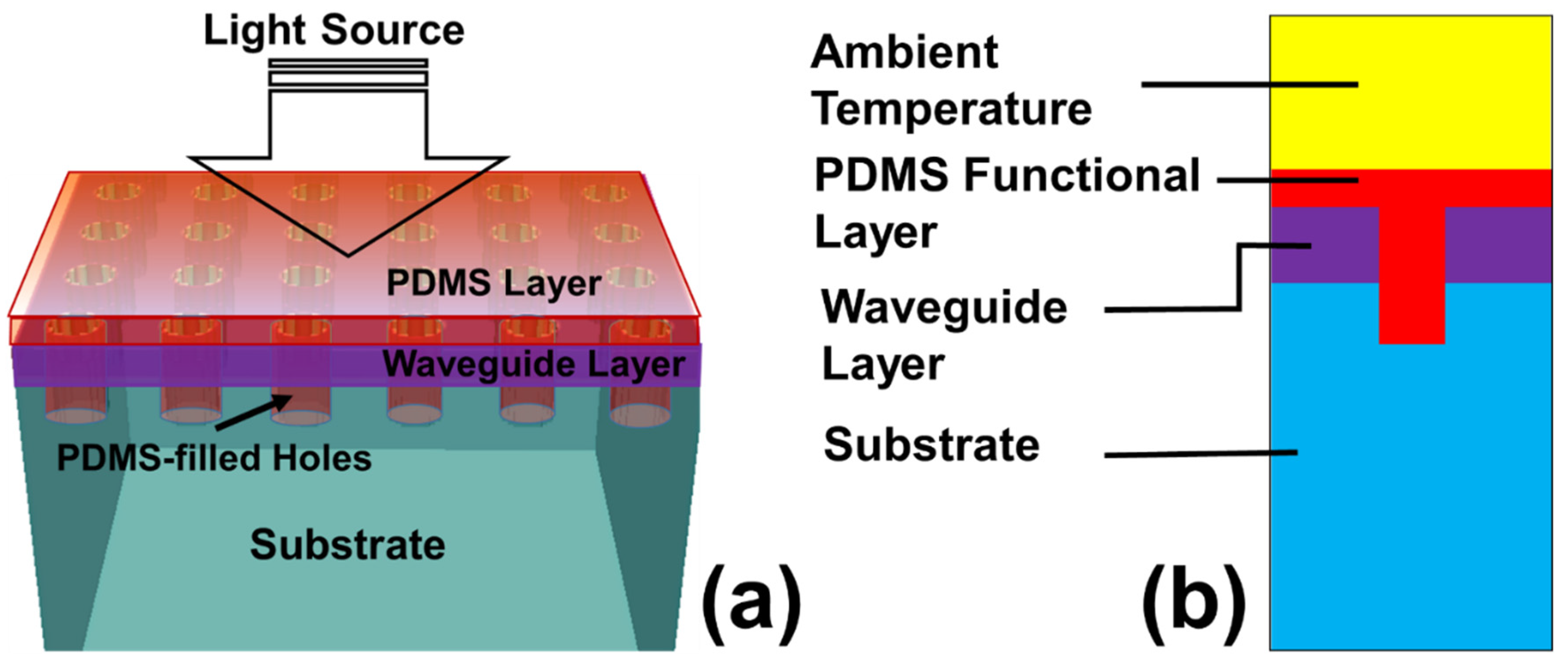
The design parameters of the PhC structure were first optimized to give a good wavelength filtering mechanism, with a narrowband Fano-resonance appearing at λ r e s = 1470 nm. As per optimized design parameters, the thickness of the waveguide was kept as t w = 330 nm, with a radius of PhC-holes as r = 200 nm. A PDMS layer was deposited on the top of the waveguide layer in the way that the PDMS material penetrates and fills the air holes. The PDMS layer was used as a functional layer, the physical properties of which vary with changes in the ambient temperature. The optimized thickness of the PDMS layer was t p = 300 nm, where the sensor gives sharp resonant peaks. A 3D model of the device is shown in Figure 2a, where the presence of the PDMS layer on the waveguide and the filling of the PDMS layer into the air holes is indicated. An incident light source placed vertically above the device, as shown, was used to excite the resonant modes. A cross-sectional view of the unit cell model can be seen in Figure 2b, with an indication of the PDMS functional layer, PDMS-filled PhC hole, and the ambient atmosphere where the temperature change was to be measured.
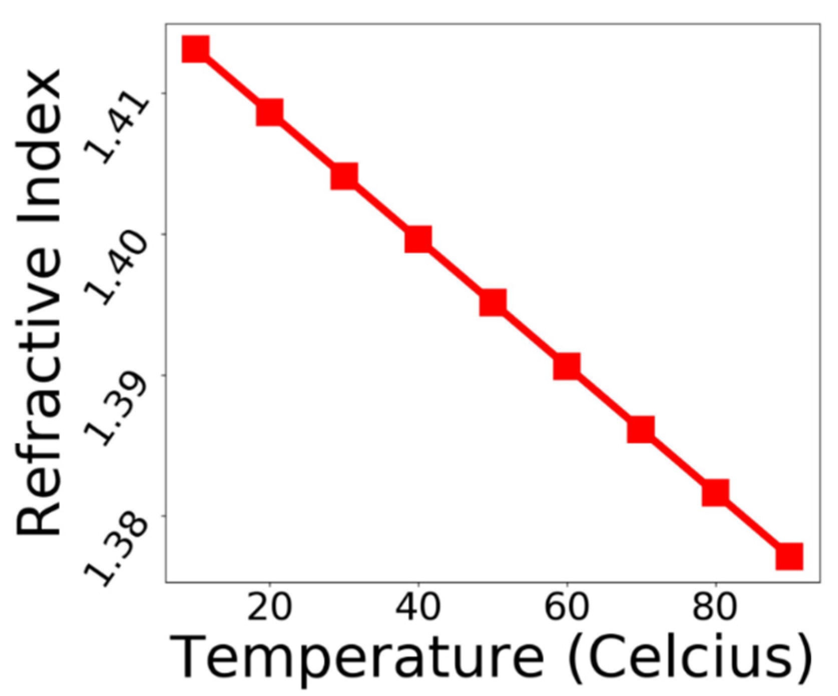
The variation in the refractive index of the PDMS material with a change in temperature T (in °C) was taken as a reference from [7,8,9], and it is given by Equation (1). The graphical representation of the above-mentioned relation is depicted in Figure 3. It can be seen that, as the temperature changes from 10 to 90 °C, the refractive index of PDMS varies linearly from 1.4131 to 1.3771. Using this relation, the designed sensor device was numerically investigated for its design and performance as an optical thermal sensor.
n p ( T ) = 1.4176 4.5 × 10 4 . T  

4. Design Parameter Optimization

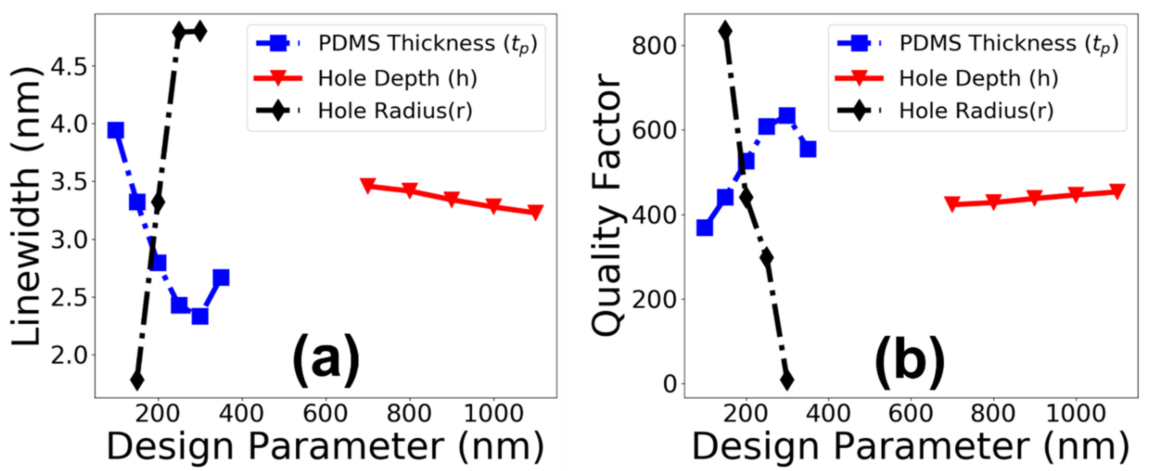
To optimize the spectral response of the proposed device to its maximum sensitivity level, the structural design parameters were varied over a range of values. The design parameters were varied, keeping in mind the minimum feature size that could be realized during the device fabrication. The two important spectral features of a GMR-based sensing device are the linewidth of the resonant modes and their quality factor (QF). Both of these spectral features were calculated for three important design parameters, i.e., thickness of the PDMS layer, depth of PhC holes, and their radius, as shown in Figure 4a,b. It is clear from the figure that the linewidth achieved its minimum values and the QF was highest around t p = 250 to 300 nm, h = 900 to 1100 nm, and r = 150 to 200 nm. However, thinking from a device-fabrication point of view, a hole-radius of 150 nm with a depth exceeding 1000 nm is challenging to fabricate and replicate with good quality. Additionally, filling PDMS material in such high aspect-ratio PhC-holes is also quite challenging. Keeping this in view, the quality of the resonant modes and the fabrication process, the optimized values of the design parameters to test the device as a thermal sensor were chosen as t p = 300 nm, h = 930 nm, and r =200 nm.

5. Testing the Device as a Thermal Sensor

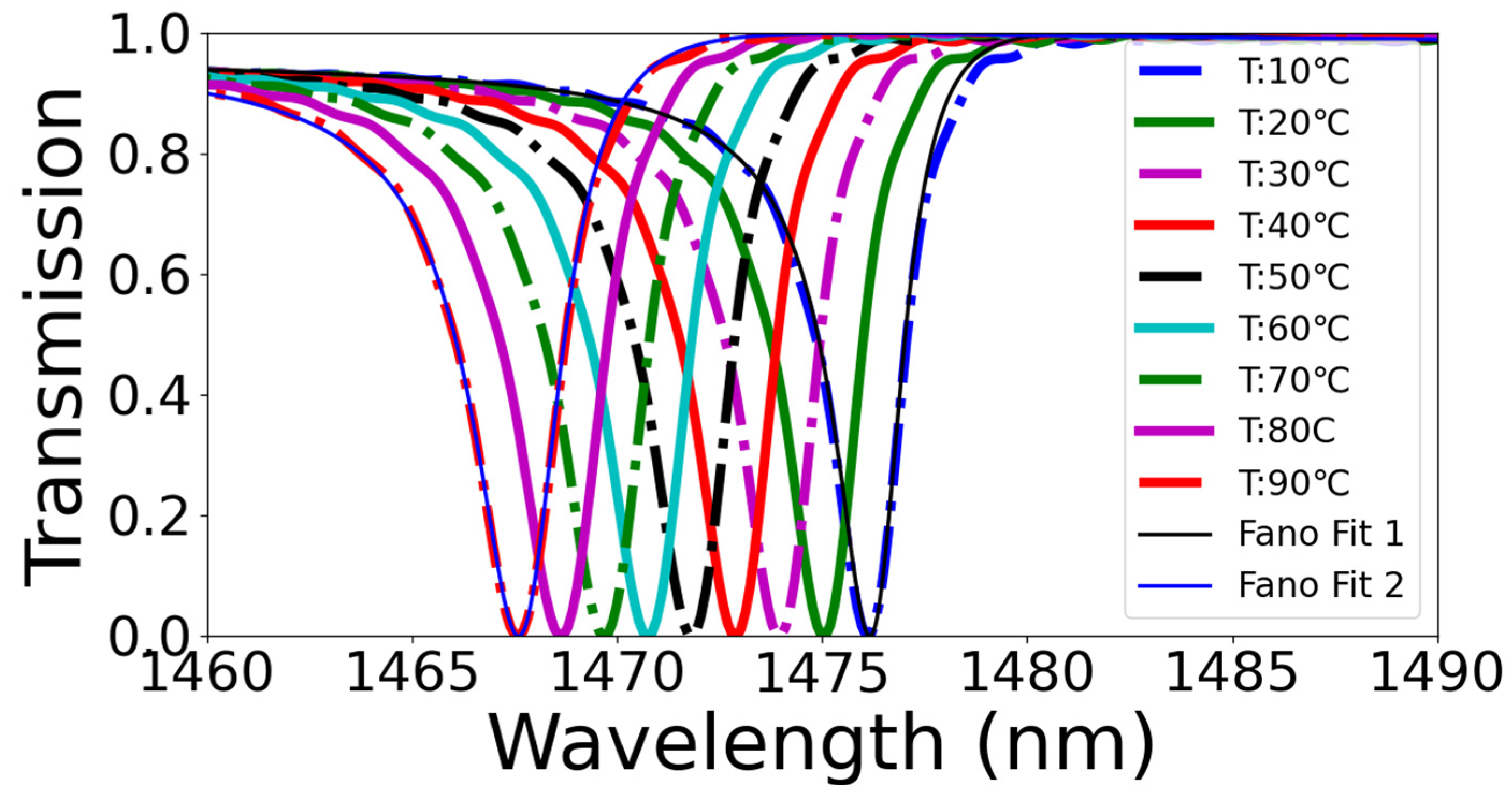
Using the relation given in Figure 3, the refractive index of the PDMS functional layer (Figure 2) was varied to investigate the performance of the designed thermal sensor. The performance of the sensor, in terms of S and FOM, was investigated for a range of design-parameter values, including   t p , h, and r. However, for sake of simplicity, the S and FOM values for two different thicknesses of PDMS, i.e., t p = 150 and 300 nm, were included. The spectral response of the sensor for t p = 300 nm is depicted in Figure 5, where it can be observed that the Fano-resonances [2] underwent a blueshift with a wavelength shift of around 0.98 nm for every 10 °C change in temperature. The response of the device was measured for an ambient temperature range of 10 to 90 °C. The first resonance for 10 °C and the last one for 90 °C were curve-fitted using the Fano lineshape function [2] to make it evident that the device purely operates on the principle of Fano-resonances. The S and FOM of the device are given by Equations (2) and (3), as follow:
S = Δ λ r e s Δ T
F O M = S Linewidth
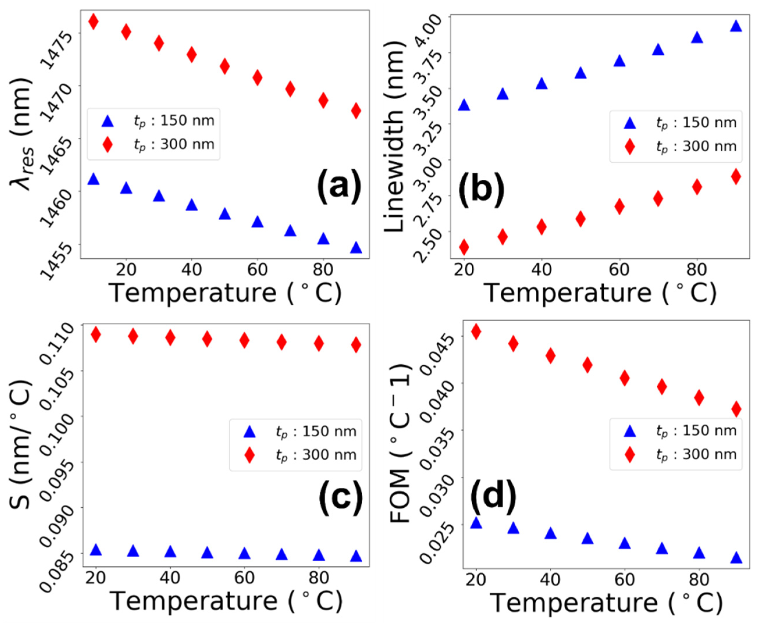
where Δ λ r e s is the change in resonant wavelength for a change in the ambient temperature   Δ T . The S and FOM of the device are expressed as nm per degree Celsius (nm/°C) and °C−1, respectively. It can be seen in Figure 6a that the resonant wavelength underwent a blueshift from 1461.18 to 1454.69 nm for t p = 150 nm and from 1476.07 to 1467.62 nm for t p = 300 nm as the ambient temperature varied from 10 to 90 °C. Moreover, the linewidth of the resonant modes in Figure 6b follows an opposite trend, where it increases from 3.38 to 3.94 nm for t p = 150 nm and from 2.39 to 2.88 for t p = 300 nm. The blueshift in the   λ r e s and an increase in the linewidth are due to the decrease in the n p of PDMS, due to which the effective refractive index n e f f of the whole periodic structure drops, resulting in the accumulation of the lower order modes. Observing the plot in Figure 6c, it can be seen that the S of the device decreases from 0.085 to 0.084 nm/°C for t p = 150 nm and from 0.109 to 0.108 for t p = 300 nm with the variation in temperature from 10 to 90 °C. Similarly, the FOM of the device in Figure 6d varies from 0.025 to 0.026 °C−1 for t p = 150 nm and from 0.045 to 0.037 °C−1 for 300 nm with a rise in the temperature and a decrease in n p .

6. Proposed Fabrication Method

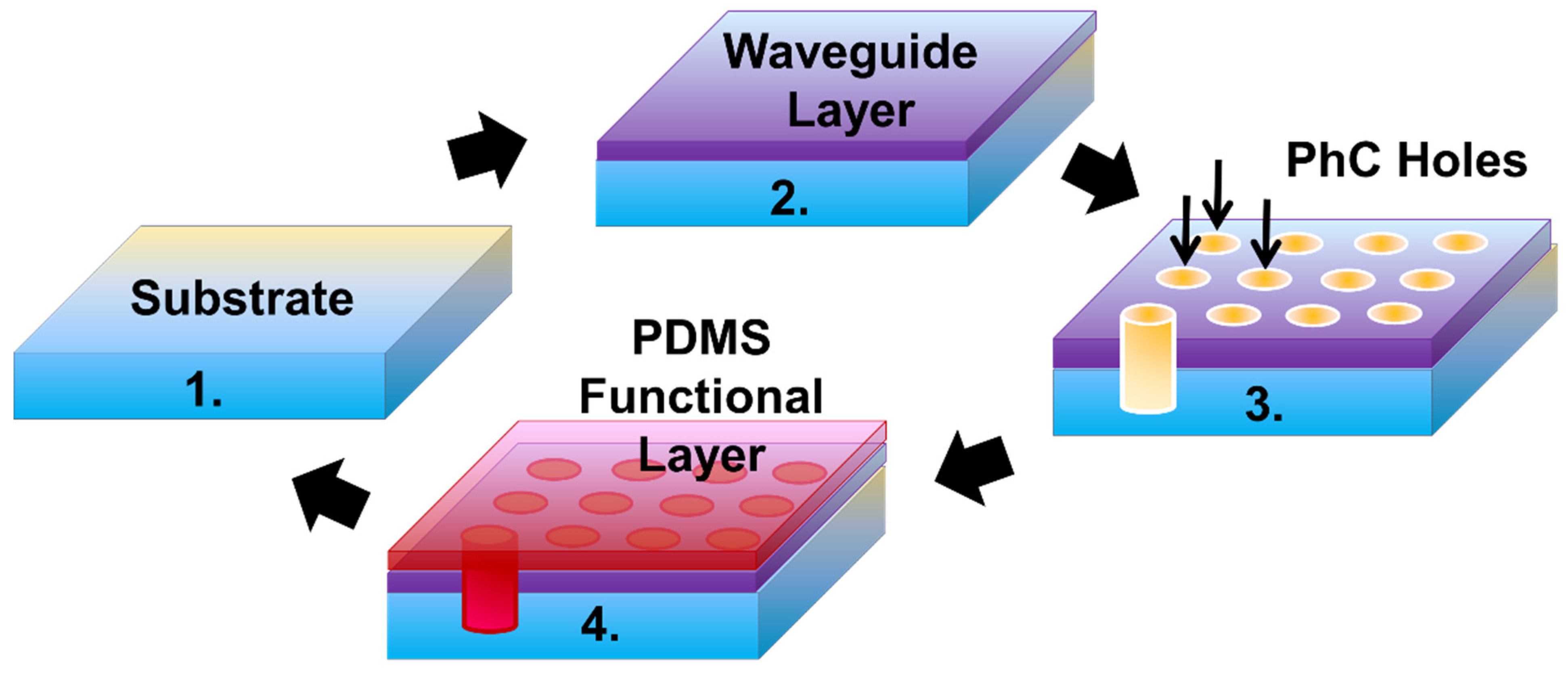
The sensor can be fabricated using conventional fabrication technologies, such as thin-film deposition, lithography, and etching techniques. A step-by-step overview of the fabrication process is shown in Figure 7. In the first step (Figure 7, step 1), a 200 nm thick waveguide layer can be deposited on top of a SiO2 glass substrate using a plasma-enhanced chemical vapor deposition (PECVD) or an ion-beam sputter deposition (IBSD) technique. A waveguide layer of Nb2O5 ( n w = 2.2) is deposited using IBSD in [2,4]. In the second step (Figure 7, step 3), the PhC grid pattern can be transferred to the substrate using electron-beam (E-beam) lithography, which offers a good resolution and fabrication quality. The holes can be etched using the conventional reactive ion etching (RIE) technique. Alternately, the PhC elements can be directly milled into the substrate using focused ion beam (FIB) milling lithography. The radius and depth of the holes can be controlled by choosing the optimum values of the software design, ion beam current, area dose, and process loops. The fabrication process of PhCs using FIB milling lithography on a borosilicate glass substrate and Nb2O5 waveguide layer is demonstrated in [2,4] for a Fano-filter and a fluid sensor, respectively. The PDMS layer can be deposited by simply pouring it onto the surface at a high temperature and spin coating it to get a uniform layer of desired thickness over the substrate (Figure 7, step 4). To remove the bubbles from liquid-state PDMS, the substrate must be put in the vacuum chamber for some time. To ensure fine-filling of the PDMS into the PhC holes and good glass-bonding, the substrate is plasma-treated [10,11,12,13]. In the literature, [43] experimentally demonstrated soft lithography to fabricate an array of PDMS nanopillars with a sub-200 nm diameter and a height of around 1000 nm using a Si master template with a nanohole array, whereas [44] reports the patterning of PDMS with nanoholes to form a protective antireflection layer using a Si mold with conical nanopillars achieving a nanohole depth in the range of 320 nm and a height of 380 nm. The sensor device can be optically characterized by using a transmission measurement setup and varying the ambient temperature.

7. Comparative Analysis

There are different categories of thermal sensors reported in the literature, such as plasmonic structures, fiber-optic-based sensors, interferometer-based designs, and periodic structures, including photonic crystals or nanogratings. Plasmonic sensors, in general, offer a higher value of sensitivity, but they are complex and expensive to fabricate. Considering the other materials for thermal sensors, dielectrics and polymers have been widely reported. Fiber-optic sensors come with an advantage of a pre-existing waveguide, and additional structures can be integrated into them for sensing. The usage of PDMS has been reported for a variety of sensing applications, including refractive index sensing, gas sensing, and thermal sensing. A comparative analysis of this work is presented in Table 1, where the already-reported thermal sensors are shortlisted, based on the usage of dielectric materials and PDMS in their design.

8. Conclusions

In conclusion, a low-cost, easy-to-implement dielectric PhCs-based thermal sensing device working in the telecommunication spectral range of 1470 nm has been numerically investigated. The device was designed on an all-solid-layered waveguide deposited on a SiO2 substrate with air-hole-based PhC holes milled across it. The proposed device operates around λ r e s = 1470 nm, with an average linewidth of 2.5 nm; the optimum design parameters were found to be the thickness of the PDMS layer as t p = 300 nm, with the depth of the PhC holes ranging from h = 900 to 1000 nm, and the radius of the holes as r = 200 nm. To sense the ambient temperature, a functional layer of PDMS with a thickness of t p = 300 nm was deposited on the top of the waveguide layer in a way that the PDMS also filled in the PhC holes. The refractive index of the PDMS decreased with a rise in the temperature. The spectral response of the sensor was numerically investigated for an ambient temperature range of 10 to 90 °C, for which the refractive index varied from 1.4131 to 1.3771. The highest S value of 0.109 nm/°C and FOM of 0.045 °C−1 were determined. Considering the inert chemical properties, temperature tolerance, and cost-effectiveness of the used dielectric materials, the sensor device can be proposed for a wide range of temperature sensing applications with easy integration with optical fiber setups.

Author Contributions

Conceptualization, Y.K. and M.A.B.; methodology, Y.K., M.A.B., S.N.K., and N.L.K.; software, M.A.B., S.N.K., and N.L.K.; validation, Y.K., M.A.B., S.N.K., and N.L.K.; formal analysis, M.A.B., S.N.K., and N.L.K.; investigation, Y.K., M.A.B., S.N.K., and N.L.K.; resources, M.A.B., S.N.K., and N.L.K.; data curation, M.A.B., S.N.K., and N.L.K.; writing—original draft preparation, Y.K., M.A.B., S.N.K., and N.L.K; writing—review and editing, Y.K. and M.A.B.; visualization, M.A.B., S.N.K., and N.L.K.; supervision, M.A.B., S.N.K., and N.L.K.; project administration, Y.K., M.A.B., S.N.K., and N.L.K.; funding acquisition, M.A.B., S.N.K., and N.L.K. All authors have read and agreed to the published version of the manuscript.

Funding

This work was financially supported by the Ministry of Science and Higher Education of the Russian Federation under the Samara National Research University in the overview and comparative parts and the FSRC “Crystallography and Photonics” of the Russian Academy of Sciences (State Task No. 007-GZ/Ch3363/26) in the part of sensing devices.

Institutional Review Board Statement

Not applicable.

Informed Consent Statement

Not applicable.

Data Availability Statement

Not applicable.

Acknowledgments

The authors are grateful to the Nanophotonics Research Group at BUITEMS Quetta for their contribution to making this research work possible.

Conflicts of Interest

The authors declare no conflict of interest.

References

  1. Limonov, M.F.; Rybin, M.V.; Poddubny, A.N.; Kivshar, Y.S. Fano resonances in photonics. Nat. Photonics 2017, 11, 543–554. [Google Scholar] [CrossRef]
  2. Khan, Y.; Rehman, A.U.; Batool, B.A.; Noor, M.; Butt, M.A.; Kazanskiy, N.L.; Khonina, S.N. Fabrication and Investigation of Spectral Properties of a Dielectric Slab Waveguide Photonic Crystal Based Fano-Filter. Crystals 2022, 12, 226. [Google Scholar] [CrossRef]
  3. Nair, R.V.; Vijaya, R. Photonic crystal sensors: An overview. Prog. Quantum Electron. 2010, 34, 89–134. [Google Scholar] [CrossRef]
  4. Khan, Y.; Butt, M.A.; Kazanskiy, N.L.; Khonina, S.N. Numerical Study of Fabrication-Related Effects of the Structural-Profile on the Performance of a Dielectric Photonic Crystal-Based Fluid Sensor. Materials 2022, 15, 3277. [Google Scholar] [CrossRef]
  5. Kazanskiy, N.L.; Butt, M.A.; Khonina, S.N. Carbon dioxide gas sensor based on polyhexamethylene biguanide polymer deposited on silicon nano-cylinders metasurface. Sensors 2021, 21, 378. [Google Scholar] [CrossRef] [PubMed]
  6. Zaky, Z.A.; Ahmed, A.M.; Shalaby, A.S.; Aly, A.H. Refractive index gas sensor based on the Tamm state in a one-dimensional photonic crystal: Theoretical optimisation. Sci. Rep. 2020, 10, 1–9. [Google Scholar] [CrossRef]
  7. Butt, M.A.; Khonina, S.N.; Kazanskiy, N.L.; Piramidowicz, R. Hybrid metasurface perfect absorbers for temperature and biosensing applications. Opt. Mater. 2022, 123, 111906. [Google Scholar] [CrossRef]
  8. Kazanskiy, N.L.; Khonina, S.N.; Butt, M.A.; Kaźmierczak, A.; Piramidowicz, R. A numerical investigation of a plasmonic sensor based on a metal-insulator-metal waveguide for simultaneous detection of biological analytes and ambient temperature. Nanomaterials 2021, 11, 2551. [Google Scholar] [CrossRef]
  9. Zhu, Z.; Liu, L.; Liu, Z.; Zhang, Y.; Zhang, Y. Surface-plasmon-resonance-based optical-fiber temperature sensor with high sensitivity and high figure of merit. Opt. Lett. 2017, 42, 2948–2951. [Google Scholar] [CrossRef] [PubMed]
  10. Friend, J.; Yeo, L. Fabrication of microfluidic devices using polydimethylsiloxane. Biomicrofluidics 2010, 4, 026502. [Google Scholar] [CrossRef] [PubMed]
  11. Choonee, K.; Syms, R.R.A.; Ahmad, M.M.; Zou, H. Post processing of microstructures by PDMS spray deposition. Sens. Actuators A: Phys. 2009, 155, 253–262. [Google Scholar] [CrossRef]
  12. Borenstein, J.T.; Tandon, V.; Tao, S.L.; Charest, J.L. (Eds.) Microfluidic Cell Culture Systems; Elsevier: Amsterdam, The Netherlands, 2018. [Google Scholar]
  13. Lötters, J.C.; Olthuis, W.; Veltink, P.H.; Bergveld, P. The mechanical properties of the rubber elastic polymer polydimethylsiloxane for sensor applications. J. Micromechanics Microengineering 1997, 7, 145. [Google Scholar] [CrossRef]
  14. Hameed, M.F.O.; Azab, M.Y.; Heikal, A.M.; El-Hefnawy, S.M.; Obayya, S.S.A. Highly sensitive plasmonic photonic crystal temperature sensor filled with liquid crystal. IEEE Photonics Technol. Lett. 2015, 28, 59–62. [Google Scholar] [CrossRef]
  15. Qian, W.; Zhao, C.L.; He, S.; Dong, X.; Zhang, S.; Zhang, Z.; Jin, S.; Guo, J.; Wei, H. High-sensitivity temperature sensor based on an alcohol-filled photonic crystal fiber loop mirror. Opt. Lett. 2011, 36, 1548–1550. [Google Scholar] [CrossRef]
  16. Peng, Y.; Hou, J.; Huang, Z.; Lu, Q. Temperature sensor based on surface plasmon resonance within selectively coated photonic crystal fiber. Appl. Opt. 2012, 51, 6361–6367. [Google Scholar] [CrossRef] [PubMed]
  17. Zou, H.; Cheng, Y. A thermally tunable terahertz three-dimensional perfect metamaterial absorber for temperature sensing application. Mod. Phys. Lett. B 2020, 34, 2050207. [Google Scholar] [CrossRef]
  18. Cai, Z.; Smith, N.L.; Zhang, J.T.; Asher, S.A. Two-dimensional photonic crystal chemical and biomolecular sensors. Anal. Chem. 2015, 87, 5013–5025. [Google Scholar] [CrossRef] [PubMed]
  19. Aly, A.H.; Mohamed, D.; Mohaseb, M.A.; Abd El-Gawaad, N.S.; Trabelsi, Y. Biophotonic sensor for the detection of creatinine concentration in blood serum based on 1D photonic crystal. RSC Adv. 2020, 10, 31765–31772. [Google Scholar] [CrossRef] [PubMed]
  20. Paternò, G.M.; Moscardi, L.; Donini, S.; Ariodanti, D.; Kriegel, I.; Zani, M.; Parisini, E.; Scotognella, F.; Lanzani, G. Hybrid one-dimensional plasmonic–photonic crystals for optical detection of bacterial contaminants. J. Phys. Chem. Lett. 2019, 10, 4980–4986. [Google Scholar] [CrossRef]
  21. Van Leest, T.; Caro, J. Cavity-enhanced optical trapping of bacteria using a silicon photonic crystal. Lab on a Chip 2013, 13, 4358–4365. [Google Scholar] [CrossRef]
  22. Murtaza, G.; Rizvi, A.S.; Irfan, M.; Yan, D.; Khan, R.U.; Rafique, B.; Xue, M.; Meng, Z.H.; Qu, F. Glycated albumin based photonic crystal sensors for detection of lipopolysaccharides and discrimination of Gram-negative bacteria. Anal. Chim. Acta 2020, 1117, 1–8. [Google Scholar] [CrossRef]
  23. Goyal, A.K.; Dutta, H.S.; Pal, S. Porous photonic crystal structure for sensing applications. J. Nanophotonics 2018, 12, 040501. [Google Scholar] [CrossRef]
  24. Xu, P.; Zheng, J.; Zhou, J.; Chen, Y.; Zou, C.; Majumdar, A. Multi-slot photonic crystal cavities for high-sensitivity refractive index sensing. Opt. Express 2019, 27, 3609–3616. [Google Scholar] [CrossRef] [PubMed]
  25. Paul, A.K.; Habib, M.S.; Hai, N.H.; Razzak, S.A. An air-core photonic crystal fiber based plasmonic sensor for high refractive index sensing. Opt. Commun. 2020, 464, 125556. [Google Scholar] [CrossRef]
  26. Cheng, Y.; Li, Z.; Cheng, Z. Terahertz perfect absorber based on InSb metasurface for both temperature and refractive index sensing. Opt. Mater. 2021, 117, 111129. [Google Scholar] [CrossRef]
  27. Cen, C.; Chen, Z.; Xu, D.; Jiang, L.; Chen, X.; Yi, Z.; Wu, P.; Li, G.; Yi, Y. High quality factor, high sensitivity metamaterial graphene—Perfect absorber based on critical coupling theory and impedance matching. Nanomaterials 2020, 10, 95. [Google Scholar] [CrossRef] [PubMed] [Green Version]
  28. Qi, Y.; Zhang, Y.; Liu, C.; Zhang, T.; Zhang, B.; Wang, L.; Deng, X.; Wang, X.; Yu, Y. A tunable terahertz metamaterial absorber composed of elliptical ring graphene arrays with refractive index sensing application. Results Phys. 2020, 16, 103012. [Google Scholar] [CrossRef]
  29. Bakir, M.; Karaaslan, M.; Dincer, F.; Akgol, O.; Sabah, C. Electromagnetic energy harvesting and density sensor application based on perfect metamaterial absorber. Int. J. Mod. Phys. B 2016, 30, 1650133. [Google Scholar] [CrossRef]
  30. Liu, X.; Zhang, X.; Liu, Y.; Liu, Z.; Peng, W. Multi-point fiber-optic refractive index sensor by using coreless fibers. Opt. Commun. 2016, 365, 168–172. [Google Scholar] [CrossRef]
  31. Zhu, J.; Lou, J. High-sensitivity Fano resonance temperature sensor in MIM waveguides coupled with a polydimethylsiloxane-sealed semi-square ring resonator. Results Phys. 2020, 18, 103183. [Google Scholar] [CrossRef]
  32. Fan, J.; Zhang, J.; Lu, P.; Tian, M.; Xu, J.; Liu, D. A single-mode fiber sensor based on core-offset inter-modal interferometer. Opt. Commun. 2014, 320, 33–37. [Google Scholar] [CrossRef]
  33. Srivastava, T.; Das, R.; Jha, R. Highly sensitive plasmonic temperature sensor based on photonic crystal surface plasmon waveguide. Plasmonics 2013, 8, 515–521. [Google Scholar] [CrossRef]
  34. Rahman, A. Temperature sensor based on dielectric optical microresonator. Opt. Fiber Technol. 2011, 17, 536–540. [Google Scholar] [CrossRef]
  35. Kong, Y.; Wei, Q.; Liu, C.; Wang, S. Nanoscale temperature sensor based on Fano resonance in metal–insulator–metal waveguide. Opt. Commun. 2017, 384, 85–88. [Google Scholar] [CrossRef]
  36. Zhao, X.; Zhang, Z.; Yan, S. Tunable Fano resonance in asymmetric MIM waveguide structure. Sensors 2017, 17, 1494. [Google Scholar] [CrossRef] [PubMed] [Green Version]
  37. Yang, X.; Hua, E.; Wang, M.; Wang, Y.; Wen, F.; Yan, S. Fano resonance in a MIM waveguide with two triangle stubs coupled with a split-ring nanocavity for sensing application. Sensors 2019, 19, 4972. [Google Scholar] [CrossRef] [PubMed] [Green Version]
  38. Fabitha, K.; Ramachandra Rao, M.S. Biocompatible miniature temperature sensor based on whispering gallery modes of Sm3+ activated ZnO optical micro-resonators. Appl. Phys. Lett. 2021, 118, 163104. [Google Scholar] [CrossRef]
  39. Batumalay, M.; Johari, M.A.M.; Khudus, M.I.M.A.; Jali, M.H.B.; Al Noman, A.; Harun, S.W. Microbottle resonator for temperature sensing. J. Phys. Conf. Ser. 2019, 1371, 012006. [Google Scholar] [CrossRef]
  40. Dong, C.H.; He, L.; Xiao, Y.F.; Gaddam, V.R.; Ozdemir, S.K.; Han, Z.F.; Yang, L. Fabrication of high-Q polydimethylsiloxane optical microspheres for thermal sensing. Appl. Phys. Lett. 2009, 94, 231119. [Google Scholar] [CrossRef]
  41. Lee, S.M.; Ahn, K.C.; Sirkis, J.S. Planar optical waveguide temperature sensor based on etched Bragg gratings considering nonlinear thermo-optic effect. KSME Int. J. 2001, 15, 309–319. [Google Scholar] [CrossRef]
  42. Lambert, E.; Fiers, M.; Nizamov, S.; Tassaert, M.; Johnson, S.G.; Bienstman, P.; Bogaerts, W. Python bindings for the open source electromagnetic simulator Meep. Comput. Sci. Eng. 2010, 13, 53–65. [Google Scholar] [CrossRef] [Green Version]
  43. Con, C.; Cui, B. Effect of mold treatment by solvent on PDMS molding into nanoholes. Nanoscale Res. Lett. 2013, 8, 1–6. [Google Scholar] [CrossRef] [PubMed] [Green Version]
  44. Lim, J.H.; Leem, J.W.; Yu, J.S. Solar power generation enhancement of dye-sensitized solar cells using hydrophobic and antireflective polymers with nanoholes. Rsc Adv. 2015, 5, 61284–61289. [Google Scholar] [CrossRef] [Green Version]
  45. Chen, Z.; Xiong, S.; Gao, S.; Zhang, H.; Wan, L.; Huang, X.; Huang, B.; Feng, Y.; Liu, W.; Li, Z. High-temperature sensor based on Fabry-Perot interferometer in microfiber tip. Sensors 2018, 18, 202. [Google Scholar] [CrossRef] [Green Version]
  46. Wu, D.; Zhao, Y.; Li, J. PCF taper-based Mach–Zehnder interferometer for refractive index sensing in a PDMS detection cell. Sens. Actuators B: Chem. 2015, 213, 1–4. [Google Scholar] [CrossRef]
  47. Yang, W.; Zhang, S.; Geng, T.; Li, L.; Li, G.; Gong, Y.; Zhang, K.; Tong, C.; Lu, C.; Sun, W.; et al. High sensitivity refractometer based on a tapered-single mode-no core-single mode fiber structure. Sensors. 2019, 19, 1722. [Google Scholar] [CrossRef] [PubMed] [Green Version]
  48. Yang, W.; Li, C.; Wang, M.; Yu, X.; Fan, J.; Xiong, Y.; Yang, Y.; Li, L. The polydimethylsiloxane coated fiber optic for all fiber temperature sensing based on the multithin–multifiber structure. IEEE Sens. J. 2020, 21, 51–56. [Google Scholar] [CrossRef]
  49. Gong, J.; Shen, C.; Xiao, Y.; Liu, S.; Zhang, C.; Ding, Z.; Deng, H.; Fang, J.; Lang, T.; Zhao, C.; et al. High sensitivity fiber temperature sensor based PDMS film on Mach-Zehnder interferometer. Opt. Fiber Technol. 2019, 53, 102029. [Google Scholar] [CrossRef]
  50. Wang, F.; Lu, Y.; Wang, X.; Ma, T.; Li, L.; Yu, K.; Liu, Y.; Li, C.; Chen, Y. A highly sensitive temperature sensor with a PDMS-coated tapered dispersion compensation fiber structure. Opt. Commun. 2021, 497, 127183. [Google Scholar] [CrossRef]
  51. Wang, H.; Liao, M.; Xiao, H.; Han, X.; Jiang, Y.; Tan, J.; Zhang, P.; Shao, J.; Tian, Y.; Yang, J. High sensitivity temperature sensor based on a PDMS-assisted bow-shaped fiber structure. Opt. Commun. 2021, 481, 126536. [Google Scholar] [CrossRef]
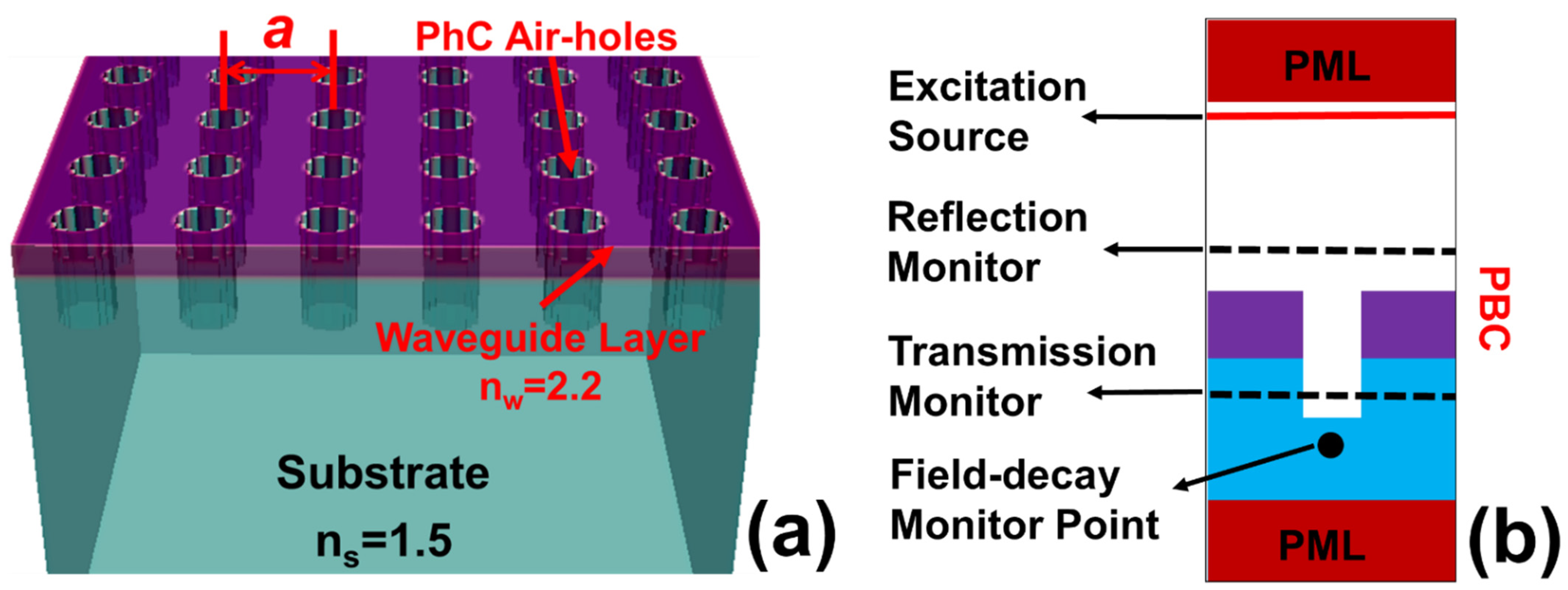
Figure 1. Numerical simulation model of the proposed thermal sensing device: (a) A 3D model of the sensor device with an indication of the substrate, waveguide layer, air holes, and lattice constant; (b) Unit cell simulation model with an indication of boundary conditions, excitation source, field monitor layer, and PhC structure.
Photonics 09 00770 g001
Figure 2. Thermal sensing mechanism of the device: (a) A PDMS functional layer was deposited on the top and filled in the PhC holes. Light source incident on the device to excite the Fano-resonances; (b) Unit cell model with PDMS functional layer and ambient atmosphere where the temperature change was to be measured.
Photonics 09 00770 g002
Figure 3. Refractive index variation of PDMS as a function of ambient temperature.
Photonics 09 00770 g003
Figure 4. (a) Design parameters vs. Linewidth; (b) Design Parameters vs. Quality Factor.
Photonics 09 00770 g004
Figure 5. Shift in the resonant modes as the ambient temperature varies from 10 to 90 °C. The first and last resonant mode is curve-fitted using the Fano-resonance lineshape function.
Photonics 09 00770 g005
Figure 6. Sensing characteristics of the device: (a)   λ r e s vs. temperature; (b) Linewidth vs. Temperature; (c) S vs. Temperature; and (d) FOM vs. Temperature.
Photonics 09 00770 g006
Figure 7. Fabrication steps for implementation of the proposed thermal sensing device.
Photonics 09 00770 g007
Table 1. Comparison of the proposed work with the existing literature.
Structure of the SensorSensitivity (nm/°C)Measurement Range (°C)Reference
Fabry–Perot interferometer on fiber tip0.01360 to 1000[45]
Photonic crystal fiber Mach–Zehnder interferometer with a PDMS detection cell0.000920 to 50[46]
Refractometer based on single-mode tapered fiber structure<0.00121 to 144[47]
PDMS-coated optic fiber0.07520 to 85[48]
Optical-fiber-,based PDMS film on Mach-Zehnder interferometer0.10120 to 100[49]
PDMS-coated, tapered optic-fiber structure0.2220 to 100[50]
PDMS-assisted, bow-shaped optic-fiber structure−1.6320 to 30[51]
PDMS-coated photonic crystal structure0.10910 to 90 This work
Publisher’s Note: MDPI stays neutral with regard to jurisdictional claims in published maps and institutional affiliations.