Abstract
Increasing the quality factor (Q-factor) of an optical resonator device has been a research focus utilized in various applications. Higher Q-factor means light is confined in a longer time which will produce a sharper peak and higher transmission. In this paper, we introduce a novel technique to further increase the Q-factor of a one-dimensional photonic crystal (1D PhC) cavity device by using an end loop-mirror (ELM). The technique utilizes and recycles the transmitted light from the conventional 1D PhC cavity design. The design has been proven to work by using the 2.5D FDTD simulation with Lumerical FDTD and MODE software. By using the ELM technique, the Q-factor of a 1D PhC design has been shown to increase up to 79.53% from the initial Q value without the ELM. The experimental result shows that the device is measurable by adding a Y-branch component to the one-port structure and able to get a high Q result. This novel design technique can be combined with any high Q-factor and very high Q-factor designs to increase more Q-factor values of photonic crystal cavity devices or any other suitable optical resonator devices.
1. Introduction
On-chip integrated optical devices have been the research focus solutions for applications such as optical communications, computing system [1], and lab-on-chip biosensing [2]. Silicon platform offers a wide range of device and component solutions for integrated designs with silicon-on-insulator (SOI) as the main material. The research focus on silicon platform is known as silicon photonics. Among the basic passive devices used in silicon-based photonic integrated circuit (PIC) designs are the photonic waveguide (photonic wire) [3], 90° bent waveguide [4], directional coupler [5], Y-branch [6], Mach–Zehnder interferometer (MZI) [7,8], ring resonator [9], and Bragg grating [10,11].
For a very precise signaling, such as for laser application, which requires very narrow resonance linewidth [12], the design requirement is to have a high quality factor (Q-factor) output. Optical resonator devices such as ring resonator, Bragg grating, and photonic crystal are the examples of high Q-factor optical devices. Another need for high Q-factor devices is for optical biosensing application, which may require a very precise measurement down to a single molecule [13]. This work focuses on one-dimensional photonic crystal (1D PhC)-based design.
The usual challenges in 1D PhC device research are to minimize the light losses and utilize the light energy effectively. The usual causes of light losses in photonic crystal devices are the light scattering at the holes [14,15] and sidewall roughness [16,17,18]. Sidewall roughness also introduces reflections along the waveguide and phase perturbations [19]. It has been shown that using a wider waveguide at 2 µm can reduce loss to 0.27 dB/cm [20]. However, this would introduce a multi-mode condition inside the waveguide. To maintain a single-mode condition in the waveguide, a 500 nm wide waveguide can be used [21].
The next challenge is to increase the Q-factor. Previous high Q-factor 1D PhC designs exploit tapered holes which reduce the modal mismatch effect [22,23], and suspend 1D PhC which increases the light confinement due to higher refractive index (RI) contrast [24]. However, this design technique also suffers longer design time because every tapered hole size change requires modification of lattice constant instead of uniform hole size design.
One thing to notice is the weakness of previous 1D PhC designs, the wasted reflected light at the holes, which divides the light in two separate directions. So, if the wasted reflected light can be recycled, making all light reflections at both directions routed to a single direction, the Q-factor and the transmission may be increased. This paper uses this concept to create a novel technique to further increase the Q-factor of a 1D PhC device. This utilizes an end loop-mirror (ELM) structure to harvest the light reflections from one side of the 1D-PhC, and direct it back to the cavity until all light from the harvested side goes back to the incoming light. This will result in a higher Q-factor and sharper peak.
This technique requires the light to be received on the same side as the incoming light source and possesses a challenge in the real application design. However, previous devices such as the Michelson interferometer [25] and micro-ring-based laser [26] have shown that it is possible to use the ELM. This suggests that the ELM can also be used to increase the Q-factor of a 1D PhC cavity device.
This novel technique and structure should be more beneficial for the multi-channel or an array of 1D PhCs because each 1D PhC will result in some light wastes that go in the opposite direction from the transmitted light. Previous research has shown that the utilization of multi-channel array of 1D PhC for WDM application [27] could utilize an additional ELM structure design technique. Another potential application from the introduced 1D PhC with the ELM structure is the photonics-based computing which has become an intense research focus now [28]. This technology will require a very high density of high Q-factor photonics devices for the purpose of very fast and precise computing. High density of high Q-factor devices will benefit from the light recycling technique to improve the Q-factor and reduce light losses.
A custom ELM design has been used. The design consideration of the loop mirror minimizes the loss of light which propagates around the loop, giving even more transmission of light from the loop back to the 1D PhC. Mathematically, it increases the light confinement time inside the cavity, and as the Q-factor formula is proportional to the light confinement time, the Q-factor increases.
The design will be simulated by using Lumerical FDTD and MODE software, and fabricated by using electron beam lithography (EBL)-based processes. The simulation results show that the design technique can increase the Q-factor of all selected 1D PhC designs which utilize uniform holes’ radius. The experimental result shows that the fabricated one-port device can be measured by adding a Y-branch to the input port and able to get a high Q transmission. This suggests that this novel design technique can increase other high Q-factor and very high Q-factor PhC designs.
2. D PhC Modeling and Q-Factor Simulations
The conventional 1D PhC structure and its geometrical parameters, which can be controlled, are shown in Figure 1. This conventional 1D PhC design uses uniform holes’ radius. The usual geometrical parameters, which can be controlled on 1D PhC design, are the lattice constant (a), cavity length (c), hole radius (r), the number of holes (N), and the width of the waveguide (W).
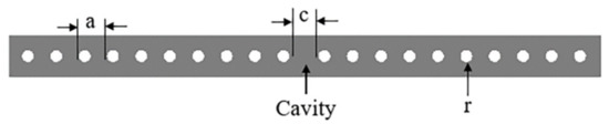
Figure 1.
The structure of one-dimensional photonic crystal (1D PhC) and its geometrical parameters.
To obtain several Q-factor results from the geometrical design changes, the simulation will use 2D FDTD solver with effective index method [29,30], also known as 2.5D FDTD. This simulation method is faster compared to 3D FDTD simulation and it is also more accurate than 2D FDTD which does not calculate the effective index of the material. To calculate the effective index value of the waveguide’s parameters used, the Eigenmode solver inside Lumerical MODE software is used. The waveguide design used is 500 nm wide and 220 nm thick. The 220 nm is a standard foundry thickness and widely used, but not necessarily an optimum thickness for all applications [21]. The simulated effective index (neff) of the waveguide design from the Eigenmode solver in Lumerical MODE is 2.4445 for fundamental TE. This neff value is used in the 2D FDTD solver in Lumerical FDTD software.
The illustration of the simulation setup for the 1D PhC is shown in Figure 2. A broadband mode source, which has a range from 1.4 to 1.7 µm, is used. The design variations target the wavelength operation at around 1.55 µm. For an ideal condition calculation, the light source is put inside the waveguide. The transmission monitor is put after the 1D PhC structure and the reflectance monitor is put behind the light source. The Q-factor monitor, which will calculate the Q-factor value, is put inside the cavity where the resonance is the strongest and is used for Q-factor comparison. Lumerical’s Q-factor monitor is used instead of manual calculation for consistency and accuracy comparisons. The Lumerical’s high Q-factor monitor calculates the Q-factor by considering the slope of the envelope of the decaying signal by using the following formula:
where fR is the resonant frequency, and m is the slope of the decay in time domain. This formula is calculated automatically by the Lumerical engine.
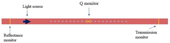
Figure 2.
The simulation setup of the 1D PhC.
Several 1D PhC cavity designs are made to calculate and compare the Q-factor values. These designs are simulated with the 2.5D FDTD method. The design details are shown in Table 1. Two variations of hole radius are used; 70 and 50 nm. The waveguide width (W) is 0.5 μm for all designs. The cavity length (c) to get the peak at the middle of the bandgap is around 386 nm. The results observed are the peak wavelength, Q-factor, and the transmission (T). These designs are chosen based on the proper selections of the design parameters by knowing how they affect the outputs [31].

Table 1.
The simulation results of the 1D PhC and the corresponding quality factor (Q-factor) value.
The results of the 2.5D FDTD simulations of the 1D PhC designs and their Q-factor are shown in Table 1. The analysis in Table 1 focuses on the effect of the design variations on the calculated Q-factor. First, increasing the number of holes (N) from 20 to 22 for 70 nm hole radius increases the Q-factor from 2409 to 4324. This is the same for 50 nm holes, where increasing the N from 40 to 46 increases the Q-factor from 8332 to 23,881. The W and peak wavelength’s effects on the Q-factors are not considered. Comparing the T and Q for each design shows that the higher Q comes from the lower T. In conclusion, the Q-factor can be increased by increasing the N, but will result in lower T. So, there is a trade-off between the Q-factor and the transmission.
The next section tests the insertion of the ELM to increase the Q-factor of each design as shown in Table 1.
3. Inserting the End Loop-Mirror (ELM) and the Effect to Q
In this section, a novel technique by using the ELM to increase the Q-factor for each design in Table 1 is tested with the same 2.5D FDTD method shown earlier. The ELM structure used has a radius of 5 μm. The insertion of the ELM’s effect is observed to the calculated Q-factor and compared with the Q-factor of the 1D-PhC without the ELM. This observation will determine whether the ELM will be able to increase the Q-factor by increasing the light confinement time inside the cavity. The illustration of the simulation layout of the 1D-PhC with the inserted ELM is shown in Figure 3. To monitor the back transmission of this one-port device, the back-transmission monitor is placed at the left of the light source that propagates to the right towards the PC cavity.
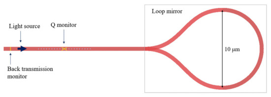
Figure 3.
1D PhC with inserted end loop-mirror (ELM) structure at one end to increase its Q value and its simulation setup.
The calculations of the transmission and reflectance spectrum from the transmission monitor for the 1D PhC structure are shown in Figure 4 and Figure 5. The back transmission for the same 1D PhC structure with the ELM is shown in Figure 6a and the mathematically manipulated result of Figure 6a is shown in Figure 6b to show it as a positive transmission. The positive transmission in Figure 6b is considered an assumption that its propagation direction is not opposite the direction of the light source propagation. This represents the result closer to the experimental situation.
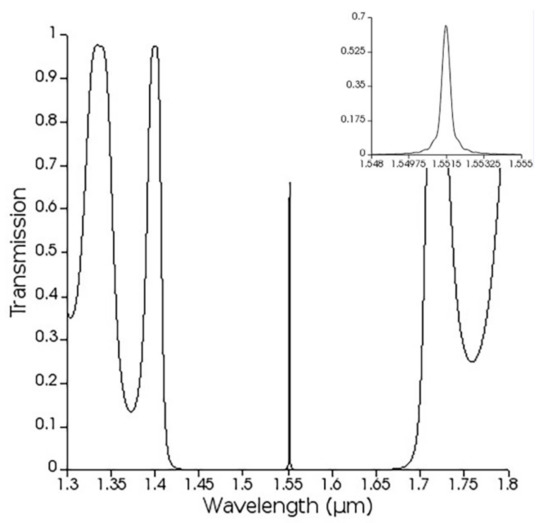
Figure 4.
The simulated transmission result of a single 1D PhC.
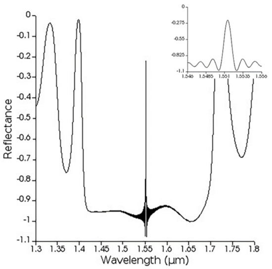
Figure 5.
The simulated reflectance result of a single 1D PhC.
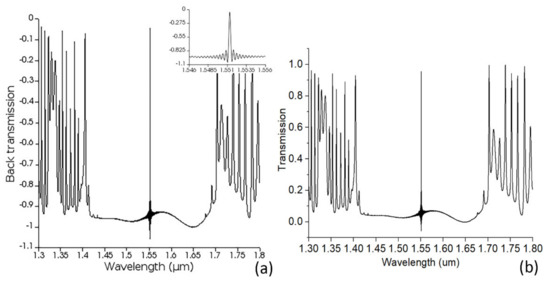
Figure 6.
The simulated results of (a) the back transmission of 1D PhC with the ELM and (b) The mathematically manipulated result of (a) for positive transmission.
The single 1D PhC transmission as shown in Figure 4 has a peak transmission of 0.636 and Q-factor of 4383, which is calculated by using the Lumerical’s Q-factor monitor from the library. The reflectance or also regarded as the back transmission of the 1D PhC structure is shown in Figure 5.
The peak transmission for the 1D PhC with the ELM as shown in Figure 6 has a negative value transmission because the transmission monitor considers the direction of the light propagation, which is considered positive for the direction of the light source propagation. The baseline as seen from the back transmission of the 1D PhC with the ELM has the same shape as from the reflectance of the 1D PhC structure, but the band-edge shapes from these two are different. It can be seen that the transmission for the 1D PhC with the ELM is higher and the inset shows a sharper peak. The calculated Q-factor is increased to 7525. It can also be observed that the base of the resonance peak of the 1D PhC with the ELM is more intense than the reflectance of the single 1D PhC. These simulation results are obvious proofs that the integration of ELM can increase the Q-factor of the 1D PhC structure. The unusual band-edge shape of the 1D PhC with the ELM can be explained with additional interferences from the reflected light and creates a band-edge shape similar to the transmission spectrum of a multi-mode interference (MMI) device [32]. The transmission modulation at the band-edge is most likely due to the separation and combination of light at different phases across the ELM.
From Table 1, it can be seen from the single 1D PhC design that higher Q-factor reduces the transmission. However, it is also shown from the 1D PhC with ELM back transmission in Figure 6a, compared with the single 1D PhC reflectance in Figure 5, that the insertion of the ELM can increase the Q-factor together with the transmission. This could be because of an extra light source compared to the conventional single 1D PhC structure.
More simulation results of the new design technique and the resulting Q-factor for designs A to D from Table 1 are shown in Table 2. Analysis of the results in Table 2 will focus on the increment of Q-factor after the insertion of the ELM from the initial Q-factor without the ELM.
Table 2.
Improvement of the Q value with the insertion of the ELM.
The highest increment of Q-factor in terms of percentage is from design A which is by 79.53%. This is because design A initially has the highest T, which is 0.77, which means more light can be recycled. The Q-factor increases from 2409 to 4325. The lowest increment is from design D which is 41.52%. The reason that design D has 41.52% improvement, which is the lowest compared to other designs, is that it initially has a very low transmission compared to others, which is 0.336. This means that the light amount for reuse from the reflection of the ELM is already low. However, in terms of the value of the Q-factor increment, design D has the highest value which is 9917. The Q-factor increases from 23,881 to 33,808.
Figure 7 shows the calculations of the electric field (E-field) map across the ELM structure at 1551 nm where the designed ELM has a calculated reflectance of 72%. Figure 8 shows the calculations of E-field map of the 1D PhC with the ELM at the resonance wavelength (1551 nm), and it can be seen that the field strength is much higher at the cavity compared to the waveguide area. The E-field map shows that the light has traveled around the ELM and will go back across the 1D PhC structure in a backward direction.
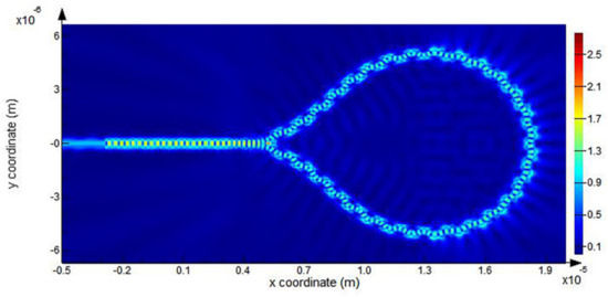
Figure 7.
The electric field map of the ELM without 1D PhC structure.
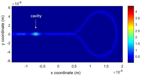
Figure 8.
The electric field map of a 1D PhC cavity structure with an ELM at resonance frequency.
The simulation results of the Q-factor improvement and the E-field profile have shown that the design concept works experimentally. However, as it is a one-port device, a correct method must be used to make it measurable. In the experimental part, it can be measured by adding a Y-branch to the device.
4. Fabrication and Measurement
As this technique results in a one-port structure, it can be measured in the real world by experimentation. This structure is shown to be measurable which will make it practical to be used. The design parameters for the reported experimental result are almost the same with design B from the simulation part. The fabrication of the device is done by Applied Nanotools Inc. The photonic devices are patterned using a Raith EBPG 5000+ electron beam instrument using a raster step size of 5 nm. The exposure dosage of the design is corrected for proximity effects that result from the backscatter of electrons from exposure to nearby features. Shape writing order is optimized for efficient patterning and minimal beam drift. An anisotropic ICP-RIE etch process is used for etching. The layout schematic of the device used for measurement is shown in Figure 9. It includes the grating couplers to couple light at input and output. A Y-branch using a SiEPIC PDK component is used to route the light into and out of the 1D PhC with the ELM. The Y-branch is one of the choices to utilize this structure. Other possible components to change the Y-branch are using the directional coupler or MMI coupler.
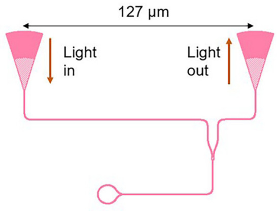
Figure 9.
The full layout schematic of the device layout with the input/output component.
The SEM image of one of the fabricated devices is shown in Figure 10. The magnification of the SEM image is 2070 times. The focused image shows the 1D PhC structure which is not visible from the larger scale. The holes’ size used for the PhC in this image is 70 nm radius which can be done with the EBL process.
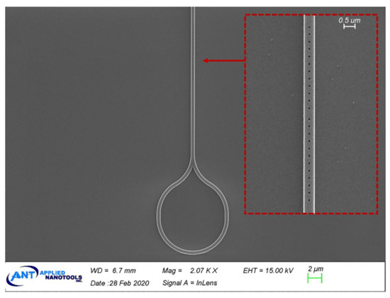
Figure 10.
SEM image of the fabricated device.
For the measurement, an Agilent 81,600B tunable laser source (TLS) is used as the light source, and an Agilent 81,635A optical power sensor is used as the output sensor. The transmission results are shown in Figure 11. The peak is at −37 dB. This transmission includes the insertion loss of grating coupler times 2 and the 50% light separation from the Y-branch, resulting in about a 3 dB drop. The transmission includes the grating coupler insertion loss. There is a bit of shift at the peak wavelength from the simulation because of the usage of the 2.5D FDTD method. By comparing the FWHM linewidth of the experimental transmission with the simulated one, the Q-factor of the experimental results is estimated to be around 4083. We use the FWHM linewidth comparison to estimate the Q-factor of the experimental result because the Lumerical Q-factor monitor uses a more complex formula than the simpler Q = fR/FWHM formula to calculate the Q-factor.
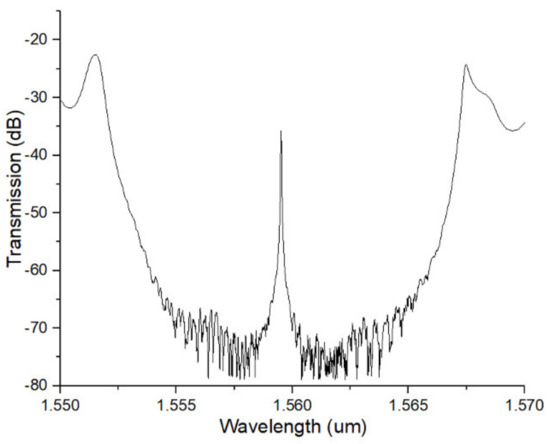
Figure 11.
The transmission result from the measurement of the 1D PhC with the ELM.
The experimental result shows that the one-port device can be measured, and the high Q transmission obtained is as expected. More research could be done in the future based on the 1D PhC with the ELM structure demonstrated in this study. Improvement of the light reflection across the ELM can also be investigated. Further analysis of this structure could be shown in future works.
5. Conclusions
The design variations of 1D PhC give different Q-factor values with the trade-off between the Q-factor and the transmission. A novel design technique has been applied by inserting an ELM to recycle the light transmission back into the 1D PhC and increase its Q-factor. The light confinement inside the one-dimensional photonic crystal cavity devices in terms of the Q-factor has been increased by inserting the loop mirror to one end of the device, reusing the light transmission from the conventional PhC device designs. This novel technique has been proven theoretically by using FDTD simulation in Lumerical FDTD software. The improvement of the Q-factor from the addition of the ELM is as high as 79.53% as shown from the simulation. The experimental result shows that the device is measurable by adding a Y-branch component to the one-port structure and able to get the desired high Q result.
Author Contributions
Conceptualization, M.H.H. and A.R.M.Z.; methodology, M.H.H.; software, A.R.M.Z.; formal analysis, M.H.H.; investigation, M.H.H. and A.R.M.Z.; resources, A.R.M.Z.; writing—original draft preparation, M.H.H.; writing—review and editing, M.H.H. and A.R.M.Z.; supervision, A.R.M.Z.; project administration, B.Y.M.; funding acquisition, B.Y.M. All authors have read and agreed to the published version of the manuscript.
Funding
This research was funded by the Malaysia Ministry of Higher Education (MOHE) for the support of this work under the FRGS/1/2020/STG02/UKM/02/2.
Institutional Review Board Statement
Not applicable.
Informed Consent Statement
Not applicable.
Data Availability Statement
Data sharing is not applicable.
Acknowledgments
We acknowledge the Applied Nanotools Inc. for the fabricated devices. We also would like to thank Lukas Chrostowski and his team for the development of the SiEPIC PDK.
Conflicts of Interest
The authors declare no conflict of interest.
References
- Absil, P.P.; Verheyen, P.; de Heyn, P.; Pantouvaki, M.; Lepage, G. Silicon photonics integrated circuits: A manufacturing platform for high density, low power optical I/O’s. Opt. Express 2015, 23, 9369–9378. [Google Scholar] [CrossRef] [PubMed]
- Song, J.; Luo, X.; Kee, J.S.; Han, K.; Li, C.; Park, M.K.; Tu, X.; Zhang, H.; Fang, Q.; Jia, L.; et al. Silicon-based optoelectronic integrated circuit for label-free bio/chemical sensor. Opt. Express 2013, 21, 2528–2533. [Google Scholar] [CrossRef]
- Dulkeith, E.; Xia, F.; Schares, L.; Green, W.M.J.; Vlasov, Y.A. Group index and group velocity dispersion in silicon-on-insulator photonic wires. Opt. Express 2006, 14, 1249–1251. [Google Scholar]
- Cherchi, M.; Ylinen, S.; Harjanne, M.; Kapulainen, M.; Aalto, T. Dramatic size reduction of waveguide bends on a micron-scale silicon photonic platform. Opt. Express 2013, 21, 819–821. [Google Scholar] [CrossRef]
- Prinzen, A.; Waldow, M.; Kurz, H. Fabrication tolerances of SOI based directional couplers and ring resonators. Opt. Express 2013, 21, 21–26. [Google Scholar] [CrossRef]
- Zhang, Y.; Yang, S.; Lim, A.E.J.; Lo, G.Q.; Galland, C.; Baehr-Jones, T.; Hochberg, M. A compact and low loss Y-junction for submicron silicon waveguide. Opt. Express 2013, 21, 1310–1316. [Google Scholar] [CrossRef]
- Mizuno, T.; Takahashi, H.; Kitoh, T.; Oguma, M.; Kominato, T.; Shibata, T. Mach—Zehnder interferometer switch with a high extinction ratio over a wide wavelength range. Opt. Lett. 2005, 30, 251–253. [Google Scholar] [CrossRef]
- Jiang, X.; Wu, J.; Yang, Y.; Pan, T.; Mao, J.; Liu, B.; Liu, R.; Zhang, Y.; Qiu, C.; Tremblay, C.; et al. Wavelength and bandwidth-tunable silicon comb filter based on Sagnac loop mirrors with Mach- Zehnder interferometer couplers. Opt. Express 2016, 24, 555–559. [Google Scholar] [CrossRef] [PubMed]
- Donzella, V.; Sherwali, A.; Flueckiger, J.; Grist, S.M.; Fard, S.T.; Chrostowski, L. Design and fabrication of SOI micro-ring resonators based on sub-wavelength grating waveguides. Opt. Express 2015, 23, 9103–9112. [Google Scholar] [CrossRef] [PubMed]
- Prabhathan, P.; Murukeshan, V.M.; Jing, Z.; Ramana, P.V. Compact SOI nanowire refractive index sensor using phase shifted Bragg grating. Opt. Express 2009, 17, 15330. [Google Scholar] [CrossRef] [PubMed]
- Donzella, V.; Sherwali, A.; Flueckiger, J.; Fard, S.T.; Grist, S.M.; Chrostowski, L. Sub-wavelength grating components for integrated optics applications on SOI chips. Opt. Express 2014, 22, 21037–21050. [Google Scholar] [CrossRef] [PubMed]
- Ishizaki, K.; de Zoysa, M.; Noda, S. Progress in photonic-crystal surface-emitting lasers. Photonics 2019, 6, 96. [Google Scholar] [CrossRef]
- Vollmer, F.; Yang, L.; Fainman, S. Label-free detection with high-Q microcavities: A review of biosensing mechanisms for integrated devices. Nanophotonics 2012, 1, 267–291. [Google Scholar] [CrossRef] [PubMed]
- Velha, P.; Rodier, J.C.; Lalanne, P.; Hugonin, J.P.; Peyrade, D.; Picard, E.; Charvolin, T.; Hadji, E. Ultra-high-reflectivity photonic-bandgap mirrors in a ridge SOI waveguide. New J. Phys. 2006, 8, 204. [Google Scholar] [CrossRef]
- Waveguides, P.C.; Ebnali-heidari, A.; Prokop, C.; Ebnali-heidari, M.; Karnutsch, C. A Proposal for Loss Engineering in Slow-Light. J. Lightwave Technol. 2015, 33, 1905–1912. [Google Scholar]
- Street, T. A theoretical analysis of scattering loss from planar optical waveguides. Opt. Quantum Electron. 1994, 26, 977–986. [Google Scholar]
- Poulton, C.G.; Koos, C.; Fujii, M.; Pfrang, A.; Schimmel, T.; Leuthold, J.; Freude, W. Radiation Modes and Roughness Loss in High Index-Contrast Waveguides. IEEE J. Sel. Top. Quantum Electron. 2006, 12, 1306–1321. [Google Scholar] [CrossRef]
- Yap, K.P.; Lapointe, J.; Lamontagne, B.; Delâge, A.; Bogdanov, A.; Janz, S.; Syrett, B. SOI Waveguide Fabrication Process Development Using Star Coupler Scattering Loss Measurements. Proc. SPIE Int. Soc. Opt. Eng. 2008, 6800, 1–12. [Google Scholar]
- Simard, A.D.; Ayotte, N.; Painchaud, Y.; Larochelle, S. Impact of Sidewall Roughness on Integrated Bragg Gratings. J. Lightwave Technol. 2011, 29, 3693–3704. [Google Scholar] [CrossRef]
- Dong, P.; Qian, W.; Liao, S.; Liang, H.; Kung, C.C.; Feng, N.N.; Shafiiha, R.; Fong, J.; Feng, D.; Krishnamoorthy, A.V. Low loss shallow-ridge silicon waveguides. Opt. Express 2010, 18, 4752–4757. [Google Scholar] [CrossRef]
- Xu, D.X.; Schmid, J.H.; Reed, G.T.; Mashanovich, G.Z.; Thomson, D.J.; Nedeljkovic, M.; Chen, X.; Van Thourhout, D.; Keyvaninia, S.; Selvaraja, S.K. Silicon Photonic Integration Platform—Have We Found the Sweet Spot? IEEE J. Sel. Top. Quantum Electron. 2014, 20, 189–205. [Google Scholar]
- Deotare, P.B.; McCutcheon, M.W.; Frank, I.W.; Khan, M.; Lončar, M. High quality factor photonic crystal nanobeam cavities. Appl. Phys. Lett. 2009, 94, 65–68. [Google Scholar] [CrossRef]
- Zain, A.R.M.; Gnan, M.; Chong, H.M.H.; Sorel, M.; de la Rue, R.M. Tapered photonic crystal microcavities embedded in photonic wire waveguides with large resonance quality-factor and high transmission. IEEE Photonics Technol. Lett. 2008, 20, 6–8. [Google Scholar] [CrossRef]
- Zain, A.R.M.; Johnson, N.P.; Sorel, M. High Quality-Factor 1-D-Suspended Photonic Crystal/Photonic Wire Silicon Waveguide Micro-Cavities. IEEE Photonics Technol. Lett. 2009, 21, 1789–1791. [Google Scholar] [CrossRef]
- Song, J.; Fang, Q.; Tao, S.H.; Liow, T.Y.; Yu, M.B.; Lo, G.Q.; Kwong, D.L. Fast and low power Michelson interferometer thermo-optical switch on SOI Abstract. Opt. Express 2008, 16, 15304–15311. [Google Scholar] [CrossRef] [PubMed]
- Zhang, Y.; Yang, S.; Guan, H.; Lim, A.E.J.; Lo, G.Q.; Magill, P.; Baehr-Jones, T.; Hochberg, M. Sagnac loop mirror and micro-ring based laser cavity for silicon-on-insulator. Opt. Express 2014, 22, 1096–1101. [Google Scholar] [CrossRef] [PubMed]
- Kuhlow, B.; Przyrembel, G.; Schlüter, S.; Fürst, W.; Steingrüber, R.; Weimann, C. Photonic crystal microcavities in SOI photonic wires for WDM filter applications. J. Light. Technol. 2007, 25, 421–431. [Google Scholar] [CrossRef]
- Alexoudi, T.; Terzenidis, N.; Pitris, S.; Moralis-Pegios, M.; Maniotis, P.; Vagionas, C.; Mitsolidou, C.; Mourgias-Alexandris, G.; Kanellos, G.T.; Miliou, A.; et al. Optics in computing: From photonic network-on-chip to chip-to-chip interconnects and disintegrated architectures. J. Light. Technol. 2019, 37, 363–379. [Google Scholar] [CrossRef]
- Hammer, M.; Ivanova, O.V. Effective index approximations of photonic crystal slabs: A 2-to-1-D assessment. Opt. Quantum Electron. 2009, 41, 267–283. [Google Scholar] [CrossRef]
- Danielmeyer, H.G.; Streifer, W.; Scifres, D.R.; Fonstad, G.; Oaks, T. The Effective Index Method and Its Application to Semiconductor Lasers. IEEE J. Quantum Electron. 1982, 18, 1083–1089. [Google Scholar]
- Haron, M.H.; Berhanuddin, D.D.; Majlis, B.Y.; Zain, A.R.M. Double-peak one-dimensional photonic crystal cavity in parallel configuration for temperature self-compensation in sensing. Appl. Opt. 2021, 60, 13–16. [Google Scholar] [CrossRef] [PubMed]
- Roth, J.; Ku, T. Low loss optical MMI-based splitter based on a semi- analytical modeling approach. Opt. Quantum Electron. 2018, 50, 1–16. [Google Scholar] [CrossRef]


Publisher’s Note: MDPI stays neutral with regard to jurisdictional claims in published maps and institutional affiliations. |
© 2021 by the authors. Licensee MDPI, Basel, Switzerland. This article is an open access article distributed under the terms and conditions of the Creative Commons Attribution (CC BY) license (https://creativecommons.org/licenses/by/4.0/).