Article

Effects of Photonic Band Structure and Unit Super-Cell Size in Graded Photonic Super-Crystal on Broadband Light Absorption in Silicon

1
Department of Physics, University of North Texas, Denton, TX 76203, USA
2
Department of Electrical Engineering, University of North Texas, Denton, TX 76203, USA
*
Author to whom correspondence should be addressed.
Photonics 2019, 6(2), 50; https://doi.org/10.3390/photonics6020050
Submission received: 9 April 2019 / Revised: 8 May 2019 / Accepted: 8 May 2019 / Published: 9 May 2019

Abstract

:
The newly discovered graded photonic super-crystal (GPSC) with a large size of unit cell can have novel optical properties that have not been explored. The unit super-cell in the GPSC can be designed to be large or small and thus the GPSC can have no photonic band gap or several gaps. The photonic band structures in Si GPSC can help predict the light absorption in Si. Photonic resonance modes help enhance the absorption of light in silicon; however, photonic band gaps decrease the absorption for light with a large incident angle. The Si device patterned in GPSC with a unit super-cell of 6a × 6a (a is a lattice constant in traditional photonic crystal) has a broadband high absorption with strong incident-angular dependence. The device with the unit super-cell of 12a × 12a has relatively low light absorption with weak incident-angle dependence. The Si GPSC with a unit super-cell of 8a × 8a combines both advantages of broadband high absorption and weak dependence of absorption on the incident angle.

1. Introduction

The traditional photonic crystal (PhC) is a periodic dielectric nano/micro-structure [1,2,3,4,5,6] with a photonic band gap and a small size of unit cell, such as a single-size Si rod in air for a two-dimensional (2D) PhC. In the past, intensive research has focused on the design and fabrication of PhCs [1]. The second-generation PhC has a unit cell of super-lattice, such as two or several different sizes of dielectric or metallic structures in air [7,8,9,10,11]. The PhC with a super-lattice unit cell can have a broad-band optical property for broad-band applications [7,8,9,10,11]. The design of PhC with a large size of unit cell was limited by the computation power of a computer central processing unit (CPU) in the past. Now the design of a PhC with a very large size of unit cell (i.e. super-cell) with graded size of rods in air is possible through parallel computations in cloud-based virtual computers [12,13,14,15,16]. We titled such a PhC as a graded photonic super-crystal (GPSC) [12,13,14,15,16,17]. The graded square-symmetric lattices form a cluster that can be arranged in 4-, 5-, or 6-fold symmetries [12,13]. A unit cell larger than 12a × 12a (a is the period of traditional PhC) can be fabricated [12,13,14].
The PhC has been used to enhance the light absorption in thin film silicon [2,3,4,5,6] besides methods of using plasmonics [18], nanowire based solar cell [19,20] and nanocone surface structuring [21,22]. The traditional PhC pattern in Si has enabled enhanced light coupling and trapping capability with a series of sharp Bloch mode resonances [2,3,4,5,6]. Using the superlattice or super-cell PhC, broadband light absorption can be achieved due to many diffraction orders provided by the PhC [7,8,9,10,11,17,23,24]. The sharp Bloch resonance peaks in the light absorption in Si patterned with the traditional PhC can be smoothed by incorporating a certain number of defects in the PhC [25,26]. By one step further from using pillar Si [27], Si patterned with quasi-random structure can have a broadband, wide incident-angle independent light absorption enhancement due to the availability of complex Fourier spectra for light coupling in the quasi-random structure [28,29,30,31,32].
In this paper, photonic band structures in the GPSC with different unit super-cell sizes was systematically studied. The light absorption in Si patterned with GPSC with different super-cell sizes was simulated. The simulation predicted that a broadband enhanced light absorption with a weak incident-angle dependence can be obtained in Si devices patterned with GPSC with a unit super-cell size of 8a × 8a.

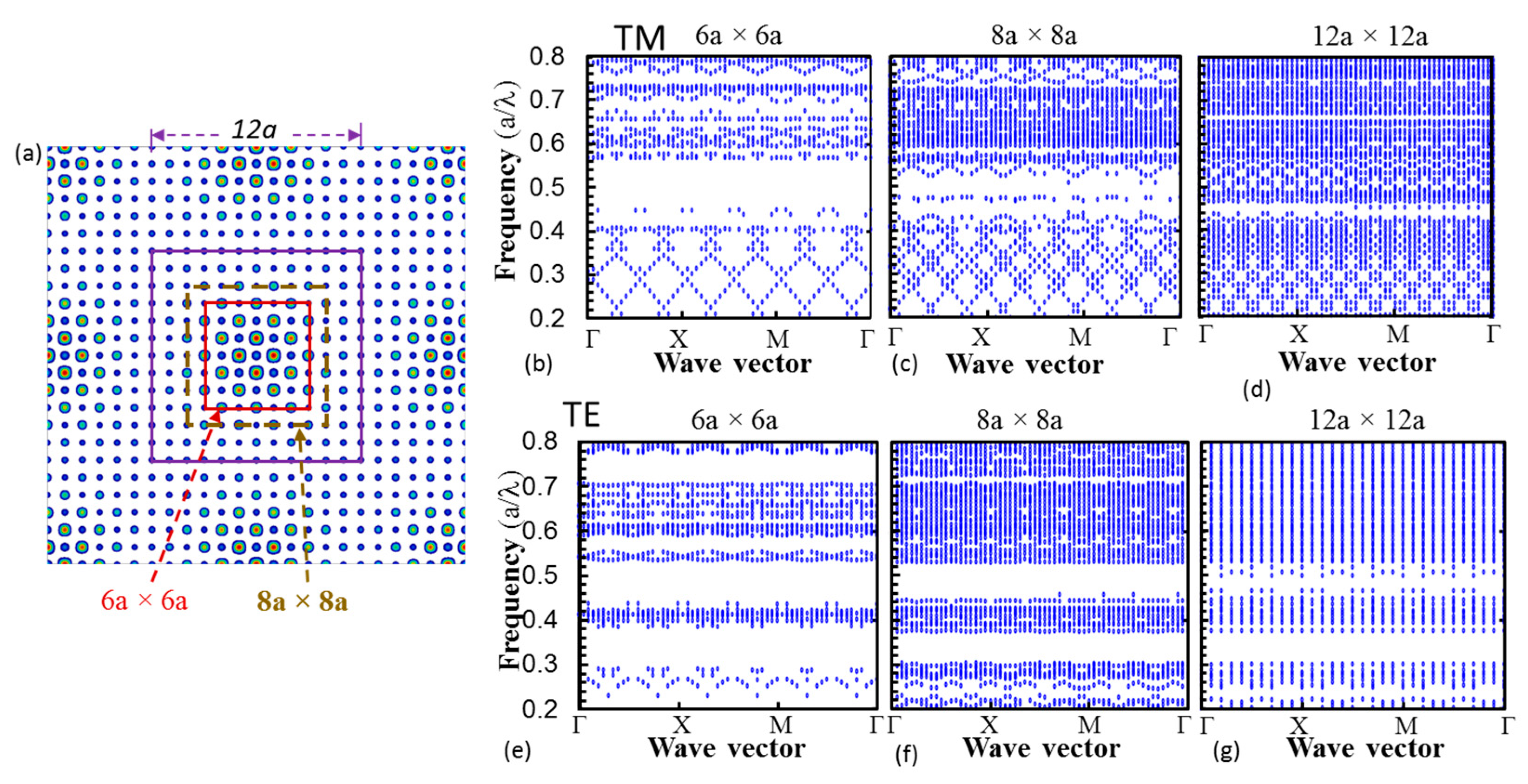
2. Photonic Band Structures in Graded Photonic Super-Crystal (GPSC) with Different Unit Cell Sizes

The GPSC can be obtained from the holographic fabrication by exposing the photoresist to the multi-beam interference pattern or using the interference pattern as an input for pattern writer for e-beam lithography. As shown in Figure 1a, the interference intensity, I(r), is determined by Equation (1), due to the eight beams.
I ( r ) = i = 1 8 E i 2 ( r , t ) + i < j 8 E i E j e i · e j c o s [ ( k j k i ) · r + ( δ j δ i ) ]
where E is the electric field, e is the electric field polarization, k is the wave vector, and δ is the initial phase. These eight-beams are separated into two sets of interfering beams. One set of interfering beams with a same intensity of I1 is arranged periodically in a cone and their wave vectors can be written as: {k1, k2, k3, k4} = {k(sin(α1)cos45°, sin(α1)cos45°, cos(α1)), k(-sin(α1)cos45°, sin(α1)cos45°, cos(α1)), k(-sin(α1)cos45°, -sin(α1)cos45°, cos(α1)), k(sin(α1)cos45°, -sin(α1)cos45°, cos(α1))}. Their initial phases are set to be 0π, 1π, 0π and 1π, respectively. The other set of interfering beams with a same intensity of I2 is arranged periodically in a cone with a much smaller cone angle of α2 than α1 and their wave vectors can be written as: {k5, k6, k7, k8} = {k(sin(α2)cos45°, sin(α2)cos45°, cos(α2)), k(-sin(α2)cos45°, sin(α2)cos45°, cos(α2)), k(-sin(α2)cos45°, -sin(α2)cos45°, cos(α2)), k(sin(α2)cos45°, -sin(α2)cos45°, cos(α2))}. Their initial phases are set to be zero. Due to the big difference between α2 and α1, these eight-beam interference pattern can be approximately understood as the square lattice with a small period of Λ1 = 2π/(k sin(α1) cos(45)) due to {k1, k2, k3, k4} modulated by beams of {k5, k6, k7, k8}. The modulation occurred over a length of Λ2 = 2π/(k sin(α2) cos(45)). The ratio of Λ21 determines the size of unit cell as an example in Figure 1a for a unit cell of 12Λ1 × 12Λ1 (the lattice constant a = Λ1). The longer the Λ2, the smaller the gradient of the lattice modulation.
There are two methods for obtaining the unit cell (for example for 6Λ1 × 6Λ1) for a GPSC. One method is to generate an interference pattern with Λ21 = 6 and the GPSC can be fabricated by laser interference lithography or e-beam lithography. The second method is to generate an interference pattern with Λ21 = 12 then cut out a unit cell of 6Λ1 × 6Λ1 in solid red square in Figure 1a as an input for E-beam pattern writer. The unit cell of 6Λ1 × 6Λ1 in Figure 1a has a smaller gradient in the circle size than that in the unit cell of directly generated interference pattern with Λ21 = 6.
Photonic band structures have been calculated in GPSC with a unit cell size of 6a × 6a, 8a × 8a and 12a × 12a in solid red square, dashed gold square and solid purple square, respectively, in Figure 1a with a = Λ1 = 350 nm. The interference pattern I(r) is converted into binary silicon/air structure: when I(r) ≥ 35% Imax (Imax is maximum in I(r)), ε(r) = dielectric constant of silicon; when I < 35%Imax, ε(r) = 1 (air). Photonic band structures were computed by using the MIT MEEP Harminv software package (Massachusetts Institute of Technology, Boston, MA, USA) [33] via the Simpetus Electromagnetic Simulation Platform in the Amazon Web Services through parallel computations in a multiple-core virtual machine. Because crystalline Si is used in 90% solar cell market share, the dielectric constant (both real and imaginary parts) [34] of crystalline silicon is used in the simulation. Figure 1b–d shows photonic band structures in TM modes in Si GPSC with a unit cell 6a × 6a, 8a × 8a, and 12a × 12a, respectively. Figure 1e–g shows photonic band structures in TE modes in Si GPSC with a unit cell 6a × 6a, 8a × 8a, and 12a × 12a, respectively.
As seen from Figure 1b–g, there are several photonic band gaps in Si GPSC with a unit cell 6a × 6a while the band gap is almost closed in that with a unit cell 12a × 12a in the frequency a/λ ranges of (0.4, 0.8) for both TE and TM modes. The photonic band gap decreases the light absorption. Because lattices of 6a × 6a is inside 8a × 8a, the light absorption in Si with these two unit cell sizes can show absorption dips at similar wavelength locations. In Figure 1b,e, there are discrete photonic bands for Bloch resonance modes that will enhance the light absorption in Si GPSC with all three unit cells. It can be predicted that the light absorption in Si GPSC with a unit cell of 12a × 12a is less than that in 6a × 6a because lattices of 6a × 6a occupy a quarter of 12a × 12a lattices, and there are photonic band gaps in 6a × 6a region and the band gap is almost closed in the other 3 quarters of the 12a × 12a region. When the incident angle is increased, the light has a stronger interaction with the photonic band gap in x-y plane than the normal incident light because the propagation of x-y component of the light is prohibited by the band gap. The photonic band structures predict that the light absorption has a stronger incident angle dependence in Si GPSC with a unit cell of 6a × 6a than that in 12a × 12a.

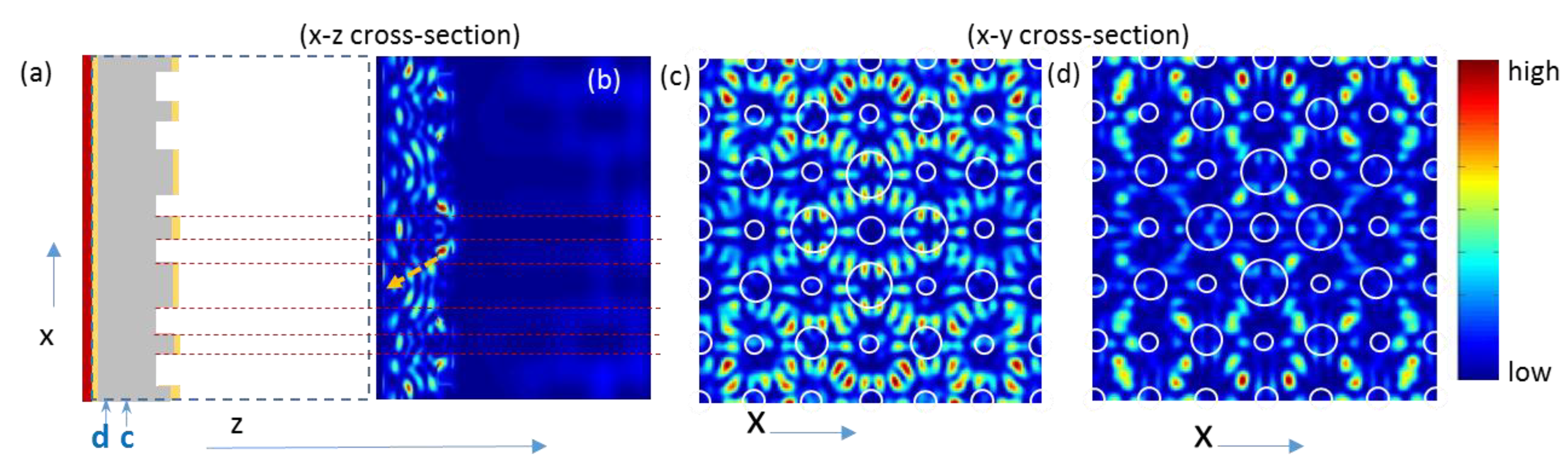
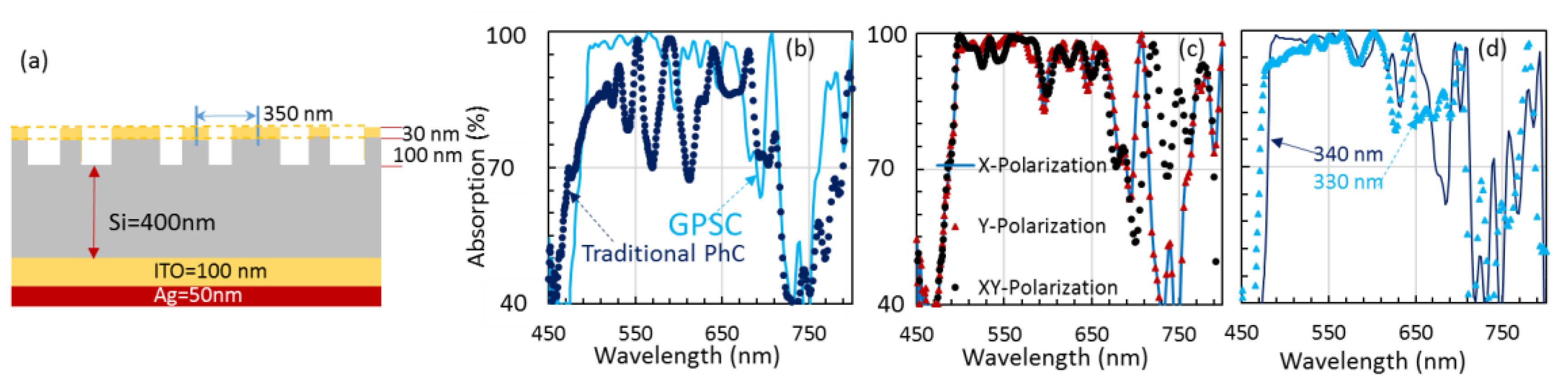
3. Broadband High Light Absorption in Si Device Patterned in GPSC

Light absorption in the silicon patterned in GPSC was simulated. Figure 2a shows a silicon device which potentially can be used as a solar cell. The 50 nm Ag was used as a reflector; 50 nm was used for a comparison with others [25]. The result is slightly different if 100 Ag is used. 100 nm ITO (n=1.8) was above the Ag film. The imaginary part of refractive index of ITO was not included for the purpose of studying the light absorption in silicon. A GPSC with a unit cell 6a × 6a (a = 350 nm and a groove depth of 100 nm) is patterned on 500 nm Si substrate as shown in Figure 2a. The dielectric constant (both real and imaginary parts) [33] of crystalline silicon was used. In the simulation, the interference intensity I(r) in Figure 1a is converted to Si if the I(r) is larger or equal to the threshold of 35% of maximum intensity (the same method that was used for the photonic band structure simulation in previous section). The GPSC can be stuck into poly(3,4-ethylenedioxythiophene) /poly(styrenesulfonate) (PEDOT:PSS) film for electrical contact for the solar cell device [35]. In this paper, we simplified the device to study the relationship between the unit cell size and the enhanced absorption in Si. Thus we put 30 nm material (yellow rectangle on top in Figure 2a) with a refractive index of 1.8 above the Si rod and air in other regions. The simulations of light absorption were also performed using MIT’s MEEP software tool [32] via the Simpetus Electromagnetic Simulation Platform in AWS. Absorption = 1-R-T. Because T=0 due to the Ag reflector in the device, the absorption was obtained from the reflection data.
Figure 2b shows light absorption both in the Si device patterned with GPSC and with the traditional PhC in a regular square lattice. The parameter of traditional PhC was chosen in such a way that the Si device patterned with PhC has a similar absorption profile as that with GPSC (i.e., rising absorption starting from 450 nm and decreasing absorption above 710 nm in Figure 2b). The absorption difference in Figure 2b is very clear: multi-peak absorption is observed in the device patterned in a traditional PhC while a broad-wavelength high absorption is observed in Si device patterned with GPSC. Figure 2c shows light absorption both in the Si device in Figure 2a for normal incident light with a polarization in x-direction (blue line), y-direction (red triangles) and x-y polarization (45 degrees relative to x) (black circles). Due to the square symmetry in the unit super-cell of 6a × 6a, it is expected that the absorption for light in x-polarization is same as that in y-polarization as shown in Figure 2c. The absorption for light in x-y polarization is almost the same as that in x-polarization except that between 710–770 nm. Usually the absorption spectrum for x-y polarization should be a linear combination of those for x and y polarizations. The difference is probably due to the dual lattice in GPSC and the photonic band gap effect because 710–770 nm (frequency a/λ of 0.49–0.5) is within the band gap in Figure 1b,e. The photonic band gap can be considered as a diffraction grating effect. The light in x-y polarization is along each lattice direction of GPSC with dual sets (high-intensity set and low-intensity set in Figure 1a of lattice basis, thus it has a higher diffraction efficiency than these in x or y-polarization with alternate high- and low-intensity lattice in Figure 1a. Due to broad spatial frequencies in the Fourier spectrum in the graded, large-size unit super-cell, the absorption is in broadband from 500 to 650 nm for light incident at 0 degrees into the Si device patterned in GPSC. There are absorption dips below 500 nm, around 595 nm, above 660 nm and below 780 nm. These dips might be caused by the photonic band gaps above 0.71, between 0.56 and 0.59, and between 0.44 and 0.53 for a/λ in Figure 1e, that are corresponding to the wavelengths below 493 nm, between 593 and 625 nm, and between 660 and 795 nm, respectively. If the lattice parameter a is decreased from 350 to 340 nm, wavelength in a/λ for one of photonic band gaps a/λ in Figure 1e (above 0.71) is approximately shifted from “below 493 nm” to “below 479 nm”. As expected, the starting wavelength for the strong absorption is shifted to 480 nm as shown in Figure 2d. When a=330 nm, the threshold wavelength for the strong absorption is blue-shifted further to 470 nm in Figure 2d.

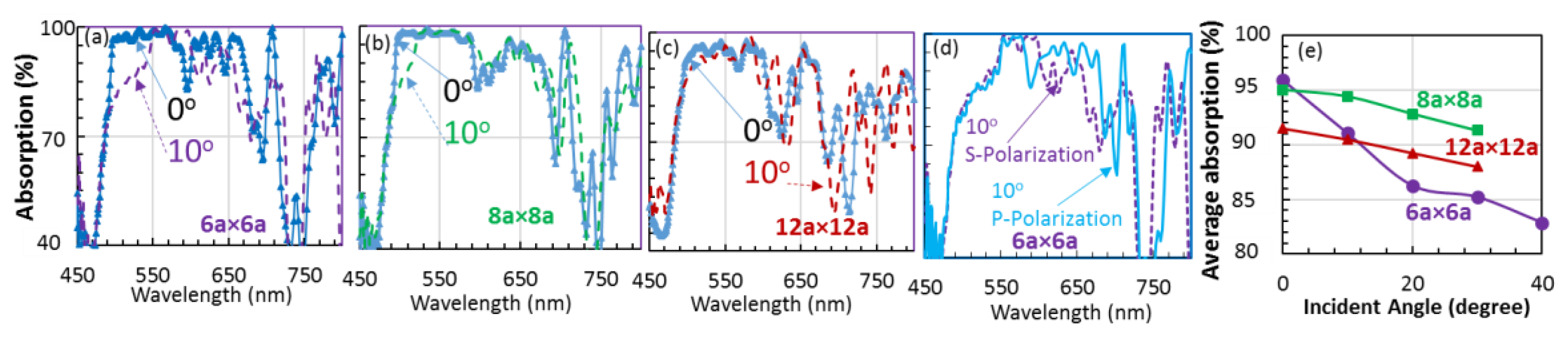
4. Unit Cell Size Effect on the Light Absorption in Si Device Patterned in GPSC

Figure 3a–c show simulated light absorption for s-polarization light incident at 0 and 10 degrees onto Si device patterned with GPSC with a = 350 nm but with a unit super-cell size of 6a × 6a, 8a × 8a and 12a × 12a, respectively. For the light incident at 0°, the absorption between 500 and 600 nm in Figure 3b in Si device patterned with GPSC with a unit cell of 8a × 8a is almost same as that with a unit cell of 6a × 6a in Figure 3a while the device with 12a × 12a (Figure 3c) has smaller absorption than these in Figure 3a,b. These results are in agreement with the prediction from the discrete band analysis in photonic band structure in previous section. For 0° incident light, the absorption dip locations in Si GPSC with a unit super-cell size of 8a × 8a in Figure 3b is almost same as that in Figure 3a with a unit cell of 6a × 6a as expected. The photonic band gap effect on the absorption are almost same for both unit cell sizes of 6a × 6a and 8a × 8a as predicted in previous section.
Figure 3d shows the light absorption in Si GPSC with a unit cell size of 6a × 6a for s-polarized and p-polarized light incident at 10 degrees. The absorption for both polarizations are almost same. Figure 3a–c shows angle dependent absorption for s-polarization only. As seen in Figure 3a, the absorption between 500 and 550 nm is reduced for light incident at 10 degrees onto Si device patterned with GPSC with a cell of 6a × 6a. The absorption in 8a × 8a in Figure 3b is reduced in a narrow range between 500 and 520 nm for the incident angle of 10 degrees while the absorption in 12a × 12a in Figure 3c is almost same for both incident angles. Figure 3e shows the average absorption between 500 and 650 nm for Si device patterned with GPSC with a unit cell size of 6a × 6a, 8a × 8a and 12a × 12a, respectively, as a function of incident angles. The Si device with 6a × 6a unit cell has a strong absorption but also a strong dependence on the incident angle (95.9% at 0° and 85% at 30°). The Si device with 12a × 12a unit cell has a weak dependence on the incident angle but has a relatively weak absorption also (91.5% at 0° and 88% at 30°). However, the Si device with 8a × 8a unit cell combines both advantages of strong absorption and weak dependence of absorption on the incident angles (95% at 0° and 91.3% at 30°). The weak dependence of absorption in Si device patterned with GPSC with a large unit cell can be understood from the following equation:
2 π λ f × n S i 2 + ( 1 f ) × n a i r 2 2 π λ sin ( θ ) = G
where nSi is the refractive index of silicon, nair is the refractive index of air, f is the fill fraction of silicon in the GPSC, λ is the wavelength in free space, and G is the reciprocal lattice vector. Due to a larger silicon filling fraction distribution in GPSC with a larger unit cell, the light can be coupled into Si GPSC in a larger angle range. Thus for solar cell application, the Si GPSC with a unit cell size of 8a × 8a can be used (the real solar spectrum has not been considered and weighted in for the calculation of the average absorption in Figure 3e). In a wide wavelength range between 450 and 700 nm, the average absorption is 83%, 83% and 81% at 0° incident angle and 74%, 80% and 77% at 30° for a Si device patterned with GPSC with a unit cell of 6a × 6a, 8a × 8a and 12a × 12a, respectively. Again, the Si device patterned with GPSC with a unit cell of 8a × 8a has a high absorption and weak angle dependence.
E-field intensity in the Si GPSC device helps us understand the simulated absorption and the light-matter interaction inside the device. Figure 4 shows the E-field intensity in the Si device patterned with the GPSC with a unit cell of 6a × 6a (a = 350 nm). Figure 4a shows the device cross-section in x-z plane at y = 0 and Figure 4b shows the E-field intensity in x-z plane at y = 0. As seen from Figure 4b, the light is diffracted into the device by the GPSC and one of light propagation directions is indicated by a dashed yellow arrow. Thus the GPSC helps coupling of free-space light into Si. Figure 4c,d shows E-field intensity for x-polarized light in the x-y plane at locations of (c,d) as labeled in Figure 4a. In Figure 4c, the E-field intensity in a region below GPSC forms well-defined patterns due to the diffraction of GPSC (or due to leaky modes in Si GPSC). E-field intensity in Figure 4d becomes weak in the middle relative to these at the top/bottom edges due to the absorption of light after it propagates deep into Si. Due to the gradient GPSC structure above the device, the absorption has a gradient distribution in the y-direction for x-polarized light.

5. Conclusions

In summary, the photonic band gap in GPSC has a strong effect on the absorption in the Si device patterned with GPSC. A strong absorption over a broad spectral and angular range has been predicted in a Si device patterned with a GPSC with a unit cell of 8a × 8a (a = 350 nm). Photonic band structures, the gradient filling fraction of Si in GPSC, and resonance modes have all played roles in the broadband light absorption in Si.

Author Contributions

Y.L. and S.H. conceived and designed simulations; S.H., K.A. and D.L. performed the simulations; Y.L. and S.H. analyzed the data and wrote the paper. All authors read and comment on the manuscript.

Funding

This work is supported by research grants from the U.S. National Science Foundation under Grant Nos. CMMI-1661842.

Conflicts of Interest

The authors declare no conflict of interest.

References

  1. Lin, Y.; Herman, P.R.; Darmawikarta, K. Design and holographic fabrication of tetragonal and cubic photonic crystals with phase mask: toward the mass-production of three-dimensional photonic crystals. Appl. Phys. Lett. 2005, 86, 071117. [Google Scholar] [CrossRef]
  2. Brongersma, M.L.; Cui, Y.; Fan, S. Light management for photovoltaics using high-index nanostructures. Nat. Mater. 2014, 13, 451–460. [Google Scholar] [CrossRef] [PubMed]
  3. Bermel, P.; Luo, C.; Zeng, L.; Kimerling, L.C.; Joannopoulos, J.D. Improving thin-film crystalline silicon solar cell efficiencies with photonic crystals. Opt. Express 2007, 15, 16986–17000. [Google Scholar] [CrossRef] [PubMed]
  4. Mallick, S.B.; Agrawal, M.; Peumans, P. Optimal light trapping in ultra-thin photonic crystal crystalline silicon solar cells. Opt. Express 2010, 18, 5691. [Google Scholar] [CrossRef] [PubMed]
  5. Bozzola, A.; Liscidini, M.; Andreani, L.C. Photonic light-trapping versus Lambertian limits in thin film silicon solar cells with 1D and 2D periodic patterns. Opt. Express 2012, 20, A224. [Google Scholar] [CrossRef] [PubMed]
  6. Park, Y.; Drouard, E.; El Daif, O.; Letartre, X.; Viktorovitch, P.; Fave, A.; Kaminski, A.; Lemiti, M.; Seassal, C. Absorption enhancement using photonic crystals for silicon thin film solar cells. Opt. Express 2009, 17, 14312. [Google Scholar] [CrossRef] [PubMed]
  7. Callahan, D.M.; Horowitz, K.A.W.; Atwater, H.A. Light trapping in ultrathin silicon photonic crystal superlattices with randomly-textured dielectric incouplers. Opt. Express 2013, 21, 30315. [Google Scholar] [CrossRef] [PubMed]
  8. Rinnerbauer, V.; Shen, Y.; Joannopoulos, J.D.; Soljačić, M.; Schäffler, F.; Celanovic, I. Superlattice photonic crystal as broadband solar absorber for high temperature operation. Opt. Express 2014, 22, A1895–A1906. [Google Scholar] [CrossRef]
  9. Rinnerbauer, V.; Lausecker, E.; Schäffler, F.; Reininger, P.; Strasser, G.; Geil, R.D.; Joannopoulos, J.D.; Soljačić, M.; Celanovic, I. Nanoimprinted superlattice metallic photonic crystal as ultraselective solar absorber. Optica 2015, 2, 743. [Google Scholar] [CrossRef]
  10. Zhang, B.; Hendrickson, J.; Guo, J. Multispectral near-perfect metamaterial absorbers using spatially multiplexed plasmon resonance metal square structures. J. Opt. Soc. Am. B 2013, 30, 656. [Google Scholar] [CrossRef]
  11. Hendrickson, J.; Guo, J.; Zhang, B.; Buchwald, W.; Soref, R. Wideband perfect light absorber at midwave infrared using multiplexed metal structures. Opt. Lett. 2012, 37, 371. [Google Scholar] [CrossRef] [PubMed]
  12. Lowell, D.; Lutkenhaus, J.; George, D.; Philipose, U.; Chen, B.; Lin, Y. Simultaneous direct holographic fabrication of photonic cavity and graded photonic lattice with dual periodicity, dual basis, and dual symmetry. Opt. Express 2017, 25, 14444–14452. [Google Scholar] [CrossRef] [PubMed]
  13. Lowell, D.; Hassan, S.; Sale, O.; Adewole, M.; Hurley, N.; Philipose, U.; Chen, B.; Lin, Y. Holographic fabrication of graded photonic super-quasi-crystals with multiple-level gradients. Appl. Opt. 2018, 57, 6598–6604. [Google Scholar] [CrossRef]
  14. Lowell, D.; Hassan, S.; Adewole, M.; Philipose, U.; Chen, B.; Lin, Y. Holographic fabrication of graded photonic super-crystals using an integrated spatial light modulator and reflective optical element laser projection system. Appl. Opt. 2017, 56, 9888. [Google Scholar] [CrossRef]
  15. Hassan, S.; Lowell, D.; Lin, Y. High light extraction efficiency in organic light-emitting diodes by patterning the cathode in graded superlattice with dual periodicity and dual basis. J. Appl. Phys. 2017, 121, 233104. [Google Scholar] [CrossRef]
  16. Hassan, S.; Sale, O.; Lowell, D.; Hurley, N.; Lin, Y. Holographic fabrication and optical property of graded photonic super-crystals with a rectangular unit super-cell. Photonics 2018, 5, 34. [Google Scholar] [CrossRef]
  17. Hassan, S.; Lowell, D.; Adewole, M.; George, D.; Zhang, H.; Lin, Y. Extraordinary light-trapping enhancement in silicon solar cell patterned with graded photonic super-crystals. Photonics 2017, 4, 50. [Google Scholar] [CrossRef]
  18. Atwater, H.A.; Polman, A. Plasmonics for improved photovoltaic devices. Nat. Mater. 2010, 9, 205–213. [Google Scholar] [CrossRef]
  19. Garnett, E.; Yang, P. Light trapping in silicon nanowire solar cells. Nano Lett. 2010, 10, 1082–1087. [Google Scholar] [CrossRef]
  20. Kelzenberg, M.D.; Boettcher, S.W.; Petykiewicz, J.A.; Turner-Evans, D.B.; Putnam, M.C.; Warren, E.L.; Spurgeon, J.M.; Briggs, R.M.; Lewis, N.S.; Atwater, H.A. Enhanced absorption and carrier collection in Si wire arrays for photovoltaic applications. Nat. Mater. 2010, 9, 239–244. [Google Scholar] [CrossRef]
  21. Han, S.E.; Chen, G. Toward the lambertian limit of light trapping in thin nanostructured silicon solar cells. Nano Lett. 2010, 10, 4692–4696. [Google Scholar] [CrossRef] [PubMed]
  22. Zhu, J.; Yu, Z.; Burkhard, G.F.; Hsu, C.-M.; Connor, S.T.; Xu, Y.; Wang, Q.; McGehee, M.; Fan, S.; Cui, Y. Optical Absorption Enhancement in Amorphous Silicon Nanowire and Nanocone Arrays. Nano Lett. 2009, 9, 279–282. [Google Scholar] [CrossRef] [PubMed]
  23. Martins, E.R.; Li, J.; Liu, Y.; Zhou, J.; Krauss, T.F. Engineering gratings for light trapping in photovoltaics: The supercell concept. Phys. Rev. B 2012, 86, 041404. [Google Scholar] [CrossRef]
  24. Wang, D.; Su, G. New strategy to promote conversion efficiency using high-index nanostructures in thin-film solar cells. Sci. Rep. 2014, 4, 7165. [Google Scholar] [CrossRef] [PubMed]
  25. Oskooi, A.; Favuzzi, P.A.; Tanaka, Y.; Shigeta, H.; Kawakami, Y.; Noda, S. Partially-disordered photonic-crystal thin films for enhanced and robust photovoltaics. Appl. Phys. Lett. 2012, 100, 181110. [Google Scholar] [CrossRef]
  26. Oskooi, A.; De Zoysa, M.; Ishizaki, K.; Noda, S. Experimental Demonstration of Quasi-Resonant Absorption in Silicon Thin Films for Enhanced Solar Light Trapping. ACS Photonics 2014, 1, 304–309. [Google Scholar] [CrossRef]
  27. Yoon, H.P.; Yuwen, Y.A.; Kendrick, C.E.; Barber, G.D.; Podraza, N.J.; Redwing, J.M.; Mallouk, T.E.; Wronski, C.R.; Mayer, T.S. Enhanced conversion efficiencies for pillar array solar cells fabricated from crystalline silicon with short minority carrier diffusion lengths. Appl. Phys. Lett. 2010, 96, 213503. [Google Scholar] [CrossRef]
  28. Martins, E.R.; Li, J.; Liu, Y.; Depauw, V.; Chen, Z.; Zhou, J.; Krauss, T.F. Deterministic quasi-random nanostructures for photon control. Nat. Commun. 2013, 4, 2665. [Google Scholar] [CrossRef]
  29. Vynck, K.; Burresi, M.; Riboli, F.; Wiersma, D.S. Photon management in two-dimensional disordered media. Nat. Mater. 2012, 11, 1017–1022. [Google Scholar] [CrossRef]
  30. Rockstuhl, C.; Fahr, S.; Bittkau, K.; Beckers, T.; Carius, R.; Haug, F.-J.; Soderstrom, T.; Ballif, C.; Lederer, F. Comparison and optimization of randomly textured surfaces in thin-film solar cells. Opt. Express 2010, 18, A335. [Google Scholar] [CrossRef]
  31. Ferry, V.E.; Verschuuren, M.A.; Van Lare, M.C.; Schropp, R.E.I.; Atwater, H.A.; Polman, A. Optimized Spatial Correlations for Broadband Light Trapping Nanopatterns in High Efficiency Ultrathin Film a-Si:H Solar Cells. Nano Lett. 2011, 11, 4239–4245. [Google Scholar] [CrossRef] [PubMed]
  32. Siddique, R.H.; Donie, Y.J.; Gomard, G.; Yalamanchili, S.; Merdzhanova, T.; Lemmer, U.; Hölscher, H. Bioinspired phase-separated disordered nanostructures for thin photovoltaic absorbers. Sci. Adv. 2017, 3, e1700232. [Google Scholar] [CrossRef]
  33. Oskooi, A.F.; Roundy, D.; Ibanescu, M.; Bermel, P.; Joannopoulos, J.D.; Johnson, S.G. MEEP: A flexible free-software package for electromagnetic simulations by the FDTD method. Comput. Phys. Commun. 2010, 181, 687–702. [Google Scholar] [CrossRef]
  34. Green, M.A. Self-consistent optical parameters of intrinsic silicon at 300 K including temperature coefficients. Sol. Energy Mater. Sol. Cells 2008, 92, 1305–1310. [Google Scholar] [CrossRef]
  35. Syu, H.-J.; Shiu, S.-C.; Lin, C. Silicon nanowire/organic hybrid solar cell with efficiency of 8.40%. Sol. Energy Mater. Sol. Cells 2012, 98, 267–272. [Google Scholar] [CrossRef]
Figure 1. (a) Simulated 8-bean interference pattern with a threshold Ith = 0.35%Imax. The purple, gold and red squares indicate the size of 12a × 12a, 8a × 8a, and 6a × 6a (the lattice constant a = Λ1), respectively, that was used as a unit cell in Si graded photonic super-crystals (GPSCs). (bd) Simulated photonic band structures in transverse magnetic (TM) modes for Si GPSCs with a unit cell of 6a × 6a, 8a × 8a, and 12a × 12a, respectively. (eg) Simulated photonic band structures in transverse electric (TE) modes for Si GPSCs with a unit cell of 6a × 6a, 8a × 8a, and 12a × 12a, respectively.
Photonics 06 00050 g001
Figure 2. (a) Schematic of a silicon device patterned with a GPSC with a unit cell of 6a × 6a (a = 350 nm). The dashed yellow indicates the top PEDOT:PSS film for a device application. (b) Absorption spectra for light (x-polarization) incident at 0° onto the silicon device patterned with GPSC, and with a traditional photonic crystal in regular square lattice. (c) Absorption spectrum for light incident at 0 degree into the device in (a) for light with x, y and x-y polarizations. (d) Absorption spectrum for x-polarized light incident at 0° into the GPSC silicon same as the one in (a) but a = 340 and 330 nm.
Photonics 06 00050 g002
Figure 3. (ac) Simulated light absorption in Si device patterned with GPSC with a unit super-cell size of 6a × 6a (a), 8a × 8a (b) and 12a × 12a (d) (a = 350 nm), respectively. (d) Shows the absorption from s-polarization and p-polarization light incident at 10 degrees for Si device patterned with GPSC with a unit super-cell size of 6a × 6a. (e) Average light absorption between 500–650 nm as a function of incident angles.
Photonics 06 00050 g003
Figure 4. (a) Schematic of x-z cross-section of Si device patterned in GPSC with a unit cell of 6a × 6a at y = 0. C and d indicate the locations in z-direction for obtaining the x-y cross-section in (c) and (d). (b) E-field intensity of x-polarized light incident at 0° onto a GPSC-patterned Si device in x-z cross-section corresponding to (a). Dashed red lines indicate the boundary between Si and air inside the Si GPSC. Dashed yellow line indicates one of light propagation path. (cd) E-field intensity in x-y cross-section in Si at z-direction locations corresponding to c and d in (a), respectively. White circles indicate the location under the GPSC Si.
Photonics 06 00050 g004

