Article

Imaging Functions of Quasi-Periodic Nanohole Array as an Ultra-Thin Planar Optical Lens

Department of Photonics and Institute of Electro-Optical Engineering, National Chiao Tung University, 1001 University Road, Hsinchu 30010, Taiwan
*
Authors to whom correspondence should be addressed.
Photonics 2015, 2(2), 619-633; https://doi.org/10.3390/photonics2020619
Submission received: 19 May 2015 / Revised: 9 June 2015 / Accepted: 9 June 2015 / Published: 12 June 2015
(This article belongs to the Special Issue New Frontiers in Plasmonics and Metamaterials)

Abstract

:
In this paper, the lensing functions and imaging abilities of a quasi-periodic nanohole array in a metal screen have been theoretically investigated and demonstrated. Such an optical binary mask with nanoholes designed in an aperiodic arrangement can function as an ultra-thin planar optical lens, imaging complex structures composed of multiple light sources at tens of wavelengths away from the lens surface. Via resolving two adjacent testing objects at different separations, the effective numerical aperture (N.A.) and the effective imaging area of the planar optical lens can be evaluated, mimicking the imaging function of a conventional lens with high N.A. Furthermore, by using the quasi-periodic nanohole array as an ultra-thin planar optical lens, important applications such as X-ray imaging and nano-optical circuits may be found in circumstances where conventional optical lenses cannot readily be applied.

1. Introduction

Nanohole arrays with quasi-periodic arrangements in metal screens exhibit intriguing optical phenomena, such as extraordinary optical transmission [1,2], subwavelength optical energy concentration [3,4,5] and polarization conversions [6,7]. Using the quasi-periodic nanohole array as an energy concentrator, Huang et al., in 2007, first demonstrated that a number of subwavelength energy hot-spots could be obtained at tens of wavelengths away from the array’s surface with a monochromatic plane wave illumination, while the generated foci were separated a few micrometers from each other [3]. In their studies, the size of the subwavelength hot-spots could be arbitrarily small within a large field of view by more sophisticated arrangement on the nanoholes. Later, in 2012, Rogers et al. successfully employed a quasi-periodic nanorings array as a focusing device in confocally scanned imaging systems, achieving the spatial resolution far beyond the optical diffraction limit [8,9,10,11]. In their imaging apparatus, the testing objects were placed several wavelengths away from the device, thus removing the main limitation of near-field instruments [12,13,14,15,16,17,18,19].
Such an optical binary mask can not only exhibit focusing ability by illuminating nanohole arrays with a plane wave, but also demonstrate the lensing performance by imaging a point source illumination on the other side of the binary mask [20,21,22]. The imaged spot moves linearly opposite to the light source displacement, giving another exploitation of a quasi-periodic nanohole array to mimic the one-to-one imaging function of a conventional lens [20]. Meanwhile, complex structures composed of multiple incoherent point sources can be distinguishably resolved via the nanoholes in quasi-periodic arrangements. This lensing performance of the nanohole arrays can be used to image tiny objects at a few tens of wavelengths away from the array onto an image plane, comparable to the imaging with conventional lenses of high numerical aperture (N.A.). By using the quasi-periodic nanohole array as an ultra-thin planar optical lens, important applications, such as X-ray imaging and nano-optical circuits, can be found in circumstances where conventional optical lenses are not readily applied. In this paper, the effective N.A. and the effective imaging area of a quasi-periodic nanohole array lens will be evaluated. Then, via imaging different testing objects composed of multiple light sources at various arrangements and wavelengths, the lensing functions and imaging abilities of the nanohole array lens will be further explored.

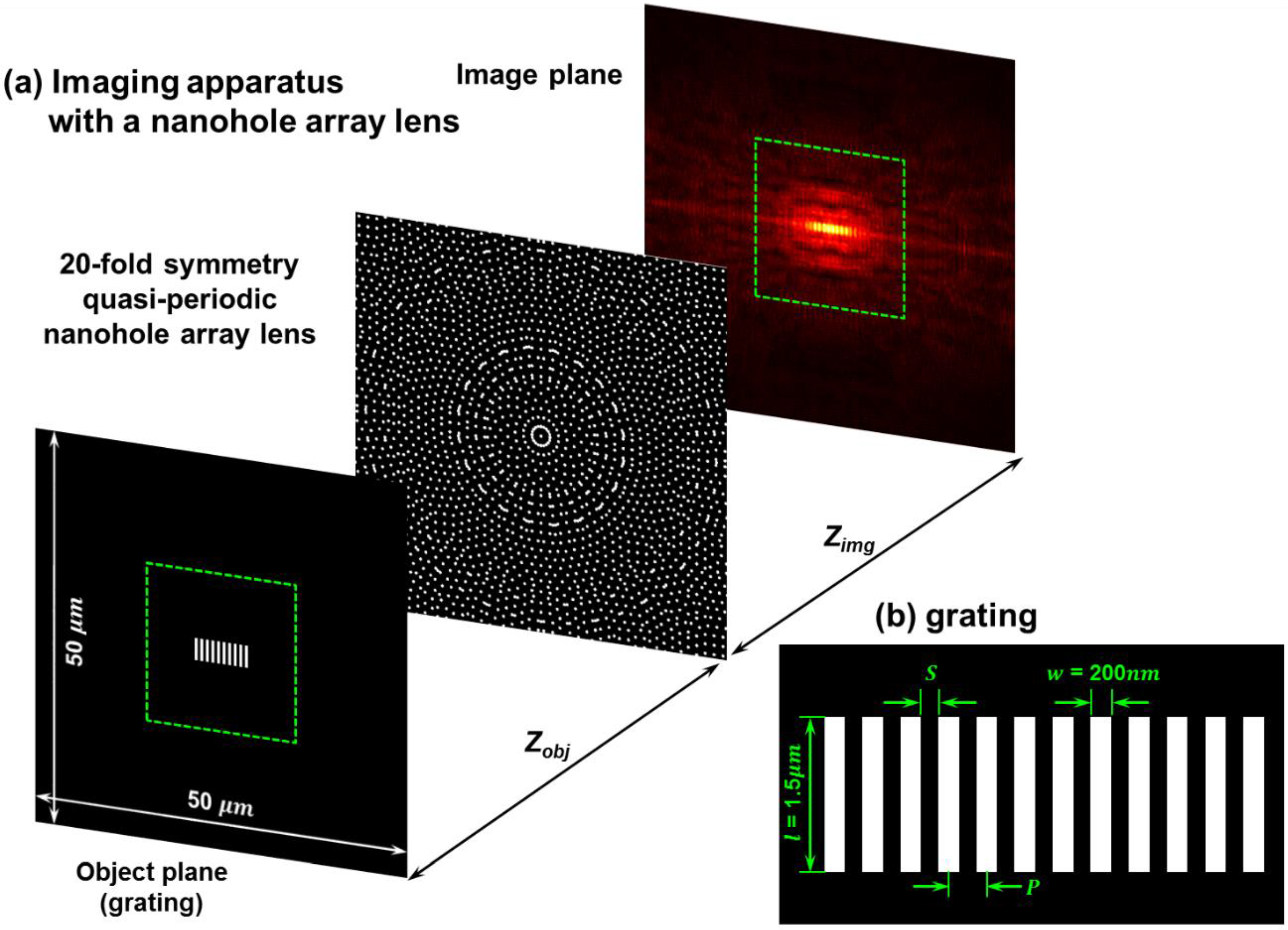
2. Imaging Abilities of a Nanohole Array Lens: Point Light Sources Illumination

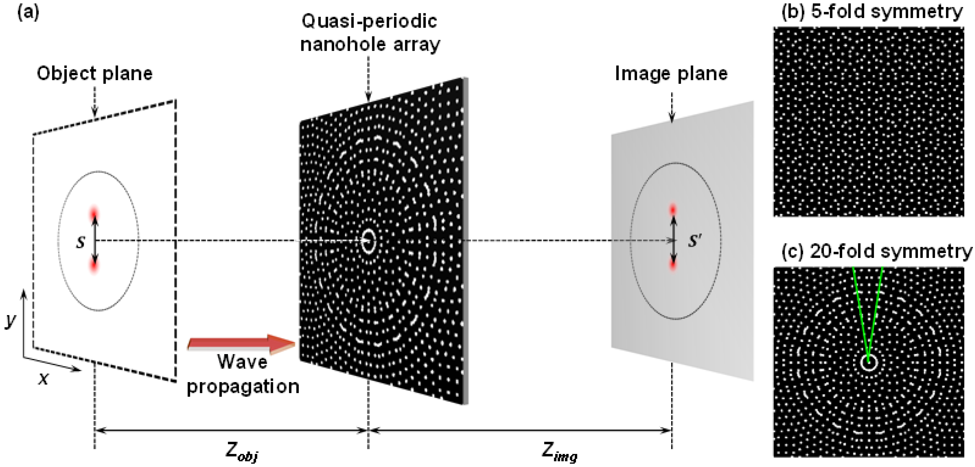
To demonstrate and compare the lensing functions of quasi-periodic nanohole arrays, a calculation model of the imaging apparatus is schematically shown in Figure 1a. Optical sources with a separation S are placed on an object plane at a distance of Zobj away from a nanohole array lens. The size of nanohole array lenses in the calculations is in an area of 50 × 50 μm2, while the illumination wavelength of the point sources is λ = 660 nm. In calculations, the scalar angular spectrum method is used to first calculate field intensity distribution on the nanohole array surface from light illuminations on the object plane [23,24]. The calculations are based on the diffraction theory employing the angular spectrum representation of the diffracted field. The diffracted field distribution at a distance Zobj away from the object plane’s surface can be expressed as:
E ( X , Y , Z ) = F ( κ x , κ y ) e i ( κ x X + κ y Y ) e i Z κ 2 κ x 2 κ y 2 d κ x d κ y ,   Z = Z o b j
where κ is the wavevector of light and Fx, κy) is the Fourier components of the electromagnetic field at the object plane, Z = 0.
By conducting the calculations again from the nanohole array’s surface, accompanied with the calculated intensity patterns, field distributions on the other side of the array will be obtained at different imaging distances Zimg. One of them may reveal an imaged pattern of the adjacent point light sources with two imaged spots separated by a distance of S′. In this paper, two types of quasi-periodic nanohole arrays—5-fold and 20-fold rotational symmetry—will be taken into account in a series of calculations. The coordinates of the quasi-periodic nanoholes are obtained by the multigrid method using JcrystalSoft Nanotube Modeler [25,26]. Quasi-periodic nanohole arrays with N-fold rotational symmetry can be obtained by converting the voids and vertices, which are constructed from N sets of parallel lines. The N sets of parallel lines are arranged overlapped, and each set is rotated by 2π/N radians. As a result, the quasi-periodic nanohole array with 5-fold rotational symmetry has a similar pattern to the Penrose tilting, as indicated in Figure 1b, showing no central optical axis in the holes’ arrangement. In the 20-fold symmetry quasi-periodic nanohole array, as the schematic fragment shown in Figure 1c, the nanohole array pattern exhibits a radially symmetric arrangement, rotated around the center by π/10 radians.
Figure 1. Imaging of two adjacent point light sources with a nanohole array lens. (a) In the model, two point light sources with a separation S are placed on an object plane at a distance of Zobj away from a nanohole array lens. In calculations, the size of nanohole array lenses is 50 × 50 μm2 and the illumination wavelength of the optical sources is λ = 660 nm. Field distributions on the other side of the nanohole array lens will be obtained at different imaging distances Zimg. Note that one of the field maps may reveal an imaged pattern with two imaged spots separated with a distance S′ which can be seen as an image of the two light sources. Plates (b) and (c) schematically show the fragments of generated quasi-periodic nanohole arrays’ patterns with 5-fold and 20-fold rotational symmetry, respectively. In (c), the angle between the two green lines is π/10 radians.
Photonics 02 00619 g001
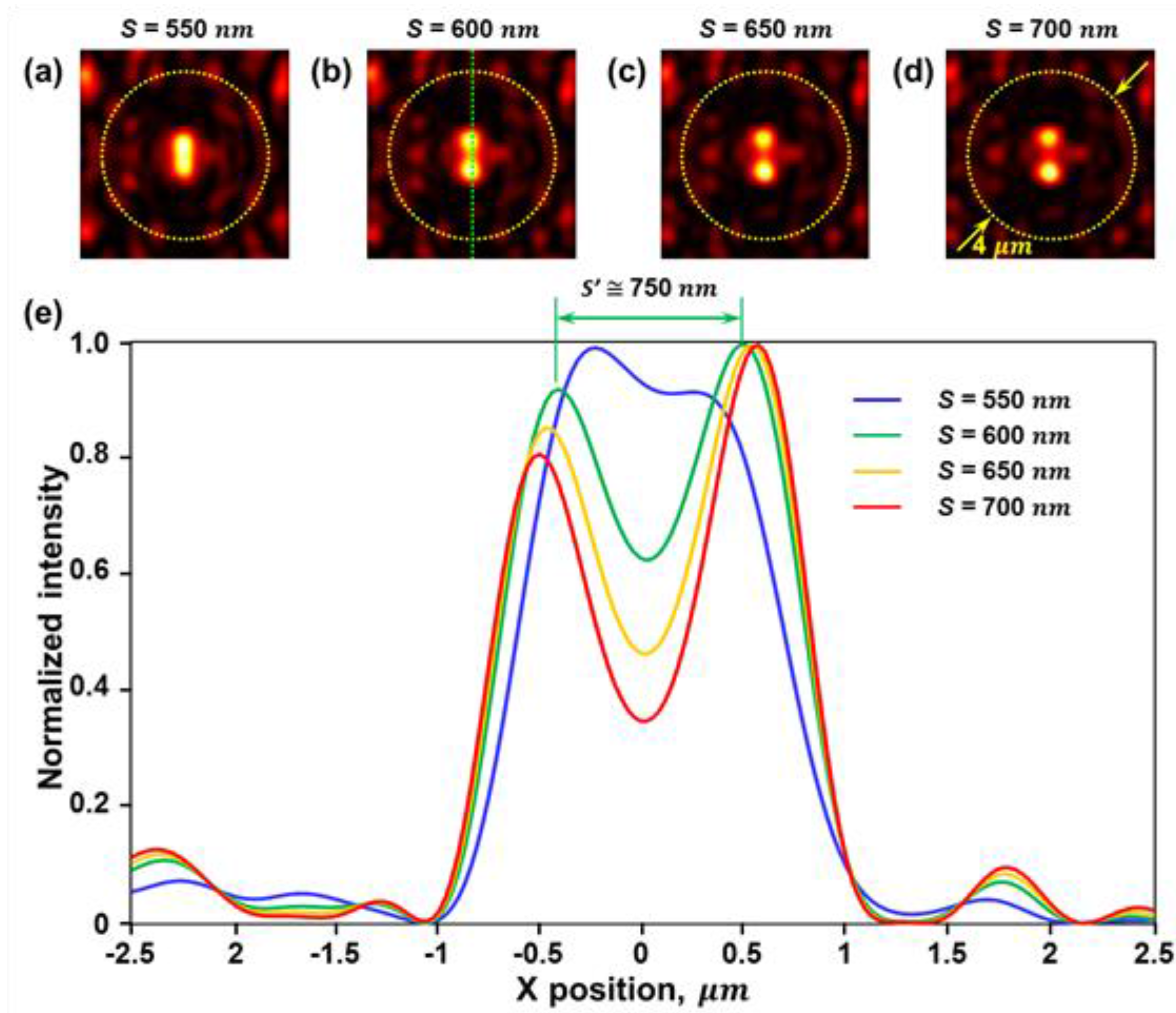
First, a 5-fold symmetry quasi-periodic nanohole array is used as a nanohole array lens to image two close point light sources with different separation distances S. The 5-fold symmetry quasi-periodic nanohole array contains about 4000 nanoholes of 200 nm in diameter and locates in an area of 50 × 50 μm2. The two adjacent point light sources are placed on an object plane at 11.4 μm away from the array’s surface for an example in the imaging demonstration, while the mid-point of the sources is on the central axis of the designed nanohole array. By using the 5-fold symmetry quasi-periodic nanohole array lens to image two separated point light sources, corresponding imaged patterns are generated on an image plane at Zimg = 11 μm as the results shown in Figure 2. In Figure 2, plates (a) to (d) display the calculation results of imaging two coherent light sources with a separation of 550 nm, 600 nm, 650 nm, and 700 nm. All the calculated imaged patterns are in a size of 5 × 5 μm2 and the yellow dashed circles indicate the estimated size of an effective imaging area of a 5-fold symmetry quasi-periodic nanohole array lens which is around 4 μm in diameter.
Figure 2. Imaging of two separated coherent point light sources by a 5-fold symmetry quasi-periodic nanohole array lens. Plates (a) to (d) show the calculated patterns of imaging two coherent light sources with a separation of 550 nm, 600 nm, 650 nm and 700 nm, respectively. The two point light sources of λ = 660 nm are placed at Zobj = 11.4 μm away from a 5-fold symmetry quasi-periodic nanohole array lens, while the imaged patterns are generated at Zimg = 11 μm. The size of the images is 5 × 5 μm2 and the yellow dashed circles indicate the effective imaging area of the quasi-periodic nanohole array lens. Plate (e) shows the cross-section profiles of the imaged spots. Note that two coherent point light sources are resolved when they are separated by S = 600 nm, while the distance between the two imaged spots is around S′ = 750 nm, giving an effective N.A. of 0.85.
Photonics 02 00619 g002
To determine whether the two optical sources can be resolved on the image plane or not, the Abbe-Rayleigh rule is applied - the two point light sources can be resolved when the central maximum of one imaged spot falls outside the location of the first minimum of the other [27]. Therefore, due to the cross-section profiles of imaged spots in the imaged patterns, as shown in Figure 2e, two coherent point light source illuminations with wavelength of 660 nm are resolved when they are separated by S = 600 nm, while a distance between the two imaged spots is around S′ = 750 nm. Regarding the incoherent illumination, as the cross-section profiles in 
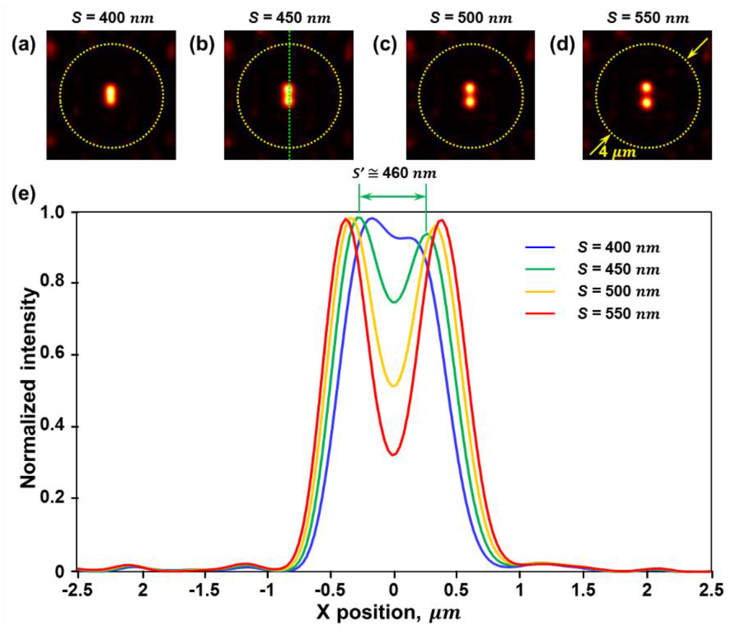
Figure 3e indicate, the imaged spots of the two separated point light sources are resolved when the sources are separated by a distance of S = 450 nm and the separation of the two imaged spots is S′ = 460 nm. It appears that a 5-fold symmetry quasi-periodic nanohole array lens shows better resolving power under incoherent illumination than coherent illumination, just as a conventional lens does. By analogy with the resolving power of a conventional lens under coherent illumination, the effective N.A. of a nanohole array lens can be given by:
N . A . = 0.77 λ S
where S′ is the resolving distance between the two imaged spots. Therefore, the 5-fold symmetry quasi-periodic nanohole array shows a resolving ability, analogous to a conventional lens of N.A. = 0.85 under incoherent illumination. Similarly, the resolving power of a conventional lens under incoherent illumination is given by:
N . A . = 0.61 λ S
In this case, the quasi-periodic nanohole array lens can function as a conventional lens with an effective N.A. = 0.89 under incoherent illumination.
Figure 3. Imaging of two separated incoherent point light sources by a 5-fold symmetry quasi-periodic nanohole array lens. Plates (a) to (d) show the calculated patterns of imaging two incoherent light sources with a separation of 400 nm, 450 nm, 500 nm and 550 nm, respectively. The two point light sources of λ = 660 nm are placed at Zobj = 11.4 μm away from a 5-fold symmetry quasi-periodic nanohole array lens, while the imaged patterns are generated at Zimg = 11 μm. The size of the images is 5 × 5 μm2 and the yellow dashed circles indicate the effective imaging area of the quasi-periodic nanohole array lens. Plate (e) shows the cross-section profiles of the two imaged spots in the imaged patterns. Note that two coherent point light sources are resolved when they are separated by S = 450 nm, while the distance between the two imaged spots is around S′ = 460 nm, giving an effective N.A. of 0.89.
Photonics 02 00619 g003
In addition, the imaging abilities of a 20-fold symmetry quasi-periodic nanohole array are also investigated through a series of calculations of the imaging of two separated point light sources. The 20-fold symmetry quasi-periodic nanohole array also contains about 4000 nanoholes in an area of 50 × 50 μm2, and the size of the nanoholes is 200 nm. As in the schematic diagram of the model shown in Figure 1, the two separated point light sources with incoherent illumination are positioned on an object plane at Zobj = 13.5 μm away from the radially symmetric quasi-periodic nanohole array lens, while imaged spots will be generated on an image plane at Zimg = 12.5 μm. The mid-point of the two incoherent point light sources is aligned with the central axis of the radially symmetric quasi-periodic nanohole array lens. In 
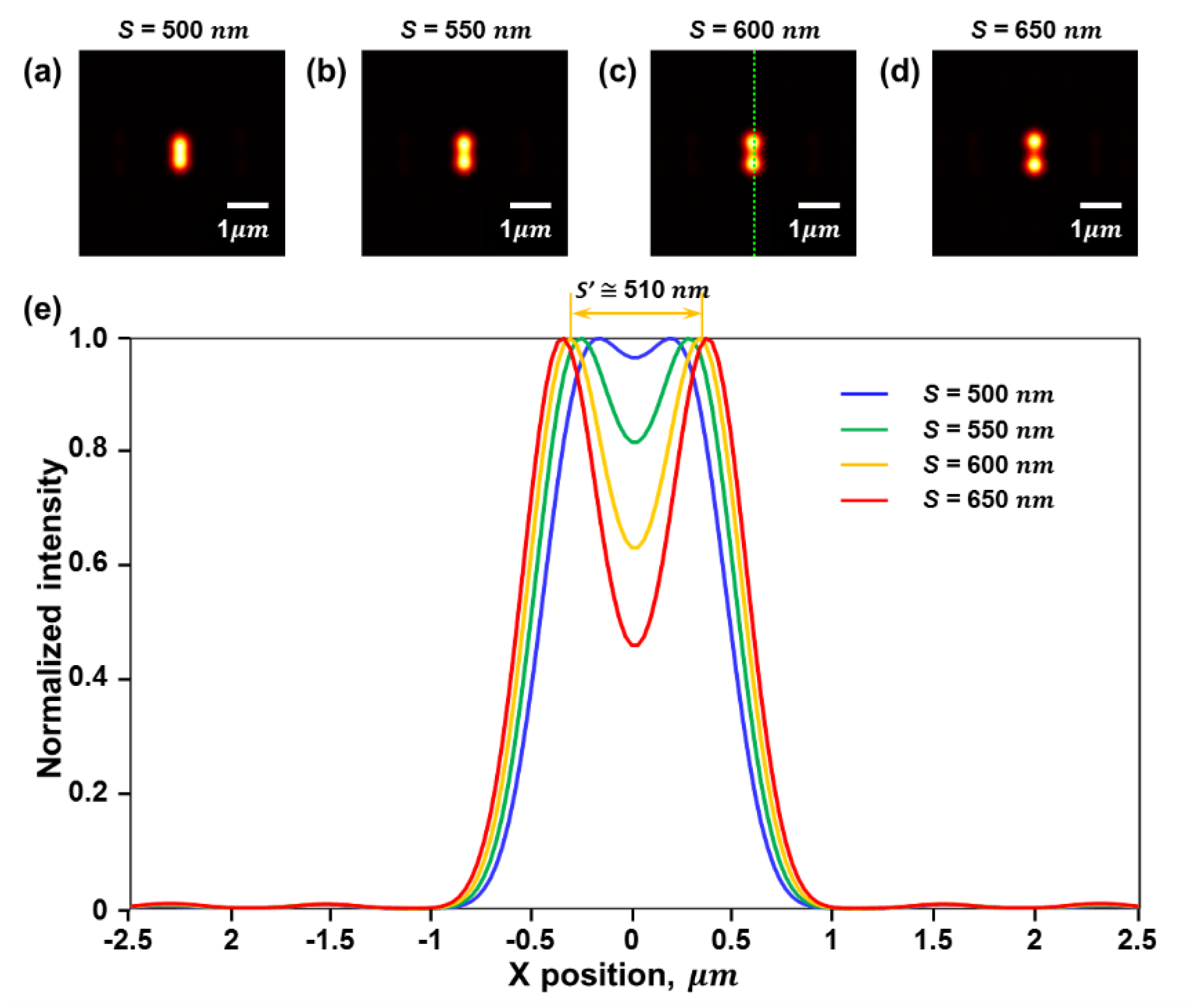
Figure 4, plates (a) to (d) display the calculation results of imaging two incoherent light source illuminations with different separations of 500 nm, 550 nm, 600 nm, and 650 nm, respectively. All the calculated imaged patterns are in a zoomed-in area of 5 × 5 μm2. The imaged patterns show that the two point light sources can be resolved when the separation between the point light sources is S = 600 nm, while the separation between the imaged spots is about S′ = 510 nm. The effective N.A. of the 20-fold symmetry quasi-periodic nanohole array lens can be estimated as around 0.67 under incoherent light illumination. Such a result indicates that the resolving power of a 20-fold symmetry quasi-periodic nanohole array lens may not be as good as that in a quasi-periodic nanohole array lens with 5-fold rotational symmetry. This may be explained by the magnification (M = Zimg/Zobj) of the 5-fold symmetry nanohole array lens in its effective imaging area. From the calculation results, it is found that the magnification of a 5-fold symmetry nanohole array lens is closer to the unitary magnification than that in a nanohole array with 20-fold rotational symmetry. Thus, with the same separation S, a 5-fold symmetry quasi-periodic nanohole array lens can separate the imaged spots with a longer displacement S′.
Figure 4. Imaging of two separated incoherent point light sources by a radially (20-fold) symmetric quasi-periodic nanohole array lens. Plates (a) to (d) show the calculated patterns of imaging two incoherent light sources with the separation of 500 nm, 550 nm, 600 nm, and 650 nm, respectively. Plate (e) shows the cross-section profiles of the two imaged spots in the imaged patterns. Note that two incoherent point light sources are resolved when they are separated by S = 600 nm, while a distance between the two imaged spots is around S′ = 510 nm, giving an effective N.A. of 0.67.
Photonics 02 00619 g004
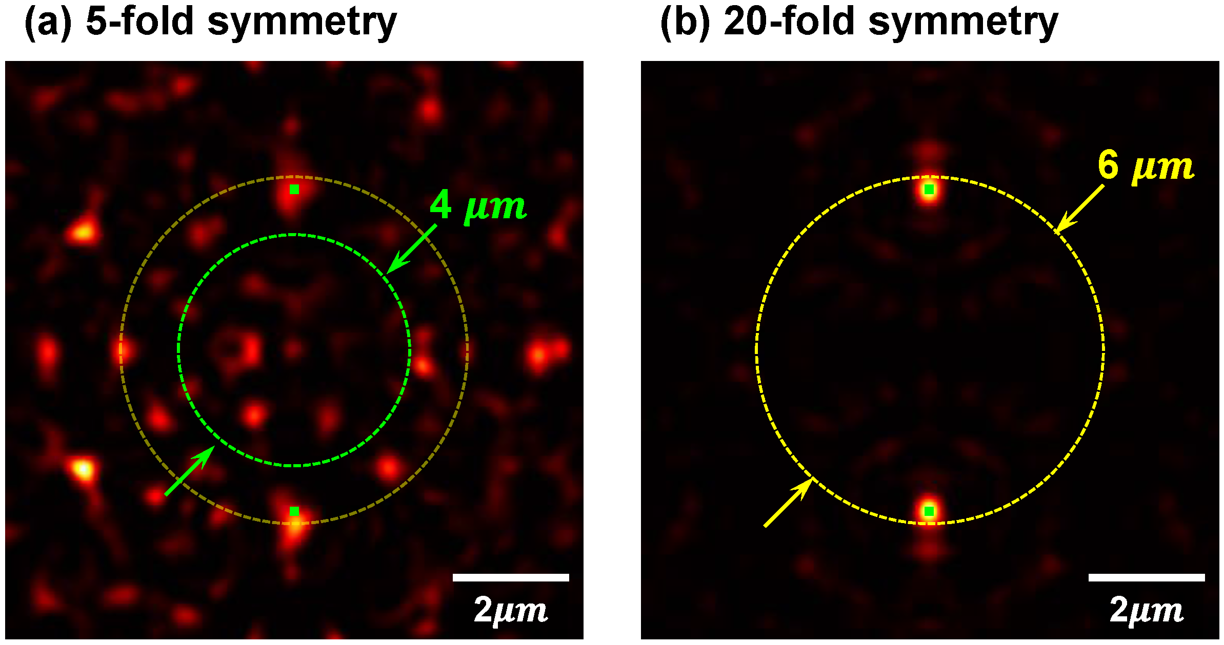
However, regarding the effective imaging area of a nanohole array lens, a larger imaging range can be obtained by a 20-fold symmetry quasi-periodic nanohole array. By separating two incoherent point light sources to 6 μm away from each other, as shown in 
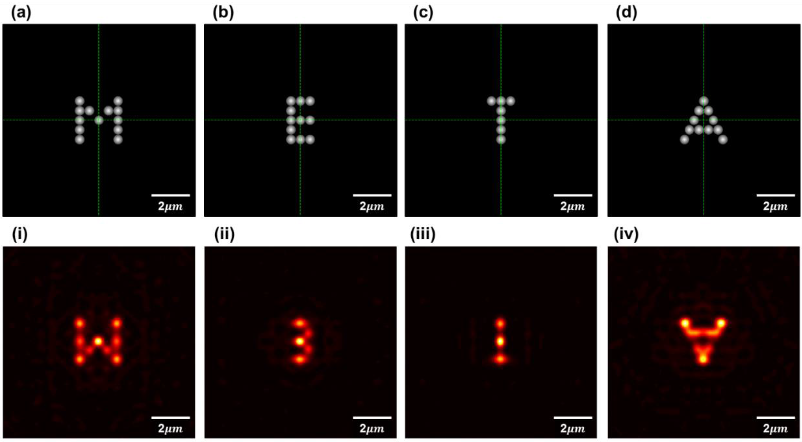
Figure 5, the imaged spots are still clearly seen because of the larger imaging area of a 20-fold symmetry quasi-periodic nanohole array lens, while a chaotic imaged pattern is obtained when a 5-fold symmetry quasi-periodic nanohole array is used. In summary, the resolving abilities of a 20-fold symmetry quasi-periodic nanohole array are not as good as that of a 5-fold symmetry quasi-periodic nanohole array lens. However, with a wide imaging area, structures, such as objects composed of multiple point light sources, slits with different lengths or grating structures, can be imaged by a 20-fold symmetry quasi-periodic nanohole array lens. A series of calculations on the imaging of different features by a 20-fold symmetry quasi-periodic nanohole array lens will be conducted and discussed in the following sections.
Figure 5. Comparison of an effective imaging area of nanohole array lenses: imaging of two separated incoherent point light sources. Plates (a) and (b) show a comparison of the effective imaging area using a 5-fold (a) and a 20-fold (b) symmetry quasi-periodic nanohole array lens, respectively. By separating the two incoherent point light sources with a separation of 6 μm, two imaged spots can still be revealed by using a 20-fold symmetry quasi-periodic nanohole array lens, indicating that a larger effective imaging area than that of a 5-fold symmetry quasi-periodic nanohole array lens.
Photonics 02 00619 g005
The lensing functions of a quasi-periodic nanohole array can also be compared to the partial reconstruction of the array’s field in the diffraction zone. Reconstruction of a quasi-periodic nanohole array’s field above the array is a complex diffraction process and the weight of the spectral maxima is varied at different distances away from the array’s surface. Therefore, with divergent light beam illumination, partial reconstruction of the array’s field will take place and the pattern of reconstructed field distributions will have the appearance of a scaled partial image of the array.
What is worth mentioning is that, at some distances, an imaged pattern representing the point light source will occur. In other words, the pattern results from a constructive interference of waves emanated from a large number of nanoholes in the array as the focused spot of a conventional lens depends on the available wave vectors of the interfering waves. When a quasi-periodic nanohole array is illuminated with a plane wave, well-defined sparsely distributed foci will be generated in the diffraction patterns. In contrast, in the case of a point-like source, a bright imaged spot will emerge in the area on the other side of the array, which is immediately opposite to the point source. If there is a relative movement between the array and the point-like source along the direction perpendicular to the axis Z, the bright imaged spot in the diffraction pattern will move accordingly to maintain the constructive interference necessary for the formation of foci. This is how a quasi-periodic nanohole array mimics the imaging function of a conventional lens. Such an optical imaging mechanism is based on the use of the quasi-periodic nanohole arrays, directly imaging the testing objects to the other side of the array lens, instead of generating superfocused energy hot-spots for the scanning apparatus [8,28,29].

3. Results and Discussion

3.1. Imaging Multiple Point Light Sources

In order to test the imaging quality with realistic objects and determine the effective imaging area of a nanohole array lens, several structures composed of multiple incoherent point light sources of λ = 660 nm are designed and placed on an object plane at Zobj = 13.5 μm away from a 20-fold symmetry quasi-periodic nanohole array lens. The structures are characters of M, E, T and A as shown in Figure 6a to d, respectively. The characters are included in an area of 2.5 × 2.5 μm2 and the central point of each character is aligned with the central axis of the array. The smallest separation distance between the light sources is 500 nm.
Figure 6. Imaging of designed structures that are composed of multiple incoherent point light sources. Plates (a) to (d) display the designed structures which are composed of multiple incoherent point light sources of λ = 660 nm as characters of M, E, T and A, respectively. The smallest distance between the point light sources is 500 nm. The designed characters are placed on an object plane at Zobj = 13.5 μm away from a 20-fold symmetry quasi-periodic nanohole array lens and the size of the structures is 2.5 × 2.5 μm2 whose central point is aligned with the central axis of the array lens. Plates (i) to (iv) show the corresponding imaged patterns but with a rotation of 180°. All the images are 10 × 10 μm2.
Photonics 02 00619 g006
By using a 20-fold symmetry quasi-periodic nanohole array as a lens to image the designed structures, calculated imaged patterns which reveal the designed characters are generated on an image plane at an optimum imaging distance of Zimg = 12.5 μm and the results are shown in Figure 6i to iv, corresponding to the designed characters as shown in the plates (a) to (d) but rotated by 180°. In the results, the appearance of the characters can be recognized but some details of the imaged spots are not distinguished. Additionally, the inhomogeneous intensity distributions on the imaged patterns indicate that the nanoholes’ distribution on the 20-fold symmetry quasi-periodic nanohole array lens is not exactly the same in all the orientations.
Furthermore, we combined the above designed characters together to create a structure over a larger area, such as the combined characters of ET and META, which are schematically shown in Figure 7a,c, respectively. The combined characters are placed on an object plane at Zobj = 13.5 μm and the central point of the structures is on the central axis of the quasi-periodic nanohole array. The size of the combined characters of ET is 6.5 × 2.5 μm2, while META is 10 × 2.5 μm2. By imaging with a 20-fold symmetry quasi-periodic nanohole array lens, the calculated imaged patterns which correspond to the structures shown in Figure 7a,c are displayed in Figure 7b,d, respectively. In the results, the imaged pattern of combined characters ET is still clearly distinguished, though some blurred patterns are generated on the edge of the pattern. In the imaged pattern of META shown in Figure 7d, in the range of effective imaging area, part of the combined characters can be imaged on the other side of the nanohole array lens. However, the imaging quality is also affected by the point light sources outside the effective imaging area and is not as good as the imaged pattern shown in plate (b).
Figure 7. Imaging of large structures composed of multiple incoherent point light sources. The designed structures of combined characters composed of multiple incoherent point light sources are placed on an object plane at Zobj = 13.5 μm away from a 20-fold symmetry quasi-periodic nanohole array lens. The combined characters of ET as shown in plate (a) are included in an area of 6.5 × 2.5 μm2, while the characters of META are in an area of 10 × 2.5 μm2 as in plate (c). Plates (b) and (d) display corresponding images to the combined characters on an image plane at Zimg = 12.5 μm.
Photonics 02 00619 g007
We also examined the quasi-periodic nanohole array lens for their imaging abilities of multiple point light sources illumination at different wavelengths. Figure 8a indicates the designed characters, E and T, composed of point light sources at wavelength of 445 nm and 484 nm, respectively. The structures are arranged on the object plane at Zobj = 13.5 μm away from the nanohole array lens surface, while Figure 8b represents the imaged pattern generated on the same image plane at an optimized distance of Zimg = 10.2 μm. In the results, the corresponding imaged pattern of the designed characters ET is still clearly distinguished but rotated by 180°, indicating that a complex system consists of multi-band fluorescent particles or multi-color nanoscale light-emitting diode (LED) components may be imaged or transferred onto an image plane at a few tens of wavelengths at the other side of the nanohole array lens.
Figure 8. Imaging of multiple incoherent point light sources at different wavelengths. (a) The designed structures of combined characters composed of multiple incoherent point light sources are placed on an object plane at Zobj = 13.5 μm, while the illumination wavelengths for the characters E and T are 445 nm and 484 nm, respectively. (b) displays corresponding imaged pattern to the combined characters on the same image plane at Zimg = 10.2 μm.
Photonics 02 00619 g008

3.2. Imaging Grating Structures Composed of Nanoslits

In addition to examining the imaging of point light sources and their various arrangements, we also tried to image other objects, such as nanoslits and their combinations with different separations. In the calculations, the illumination wavelength is assumed to be λ = 660 nm and the central point of each object is on the central axis of the nanohole array lens. The test object parameters are as follows: l denotes the length of nanoslits and w is the width, separation S is the edge-to-edge distance between two adjacent nanoslits and the period P = w + S of a grating structure is the center-to-center distance of the constituent nanoslits as shown in Figure 9b.
The imaging of grating structures by a 20-fold symmetry quasi-periodic nanohole array lens is schematically shown in Figure 9. The grating structures contain 12 nanoslits and are placed on an object plane at 13.5 μm away from the quasi-periodic nanohole array lens. The length and width of each nanoslit are fixed at l = 1.5 μm and w = 200 nm, respectively. The grating periods P between the constituent nanoslits are 600 nm and 650 nm, indicating that the overall areas of the two designed gratings are 6.8 × 1.5 μm2 and 7.35 × 1.5 μm2. The geometric center of the grating structures is aligned with the central axis of the nanohole array lens.
Figure 9. Imaging of gratings by a 20-fold symmetry quasi-periodic nanohole array lens. (a) shows the imaging of grating structures by using a 20-fold symmetry quasi-periodic nanohole array, while (b) schematically displays the grating structures. The grating structures are placed on an object plane at Zobj = 13.5 μm. The length and width of each nanoslit are fixed at l = 1.5 μm and w = 200 nm, respectively. The grating periods P between the constituent nanoslits are 600 nm and 650 nm, indicating that the overall areas of the two designed gratings are 6.8 × 1.5 μm2 and 7.35 × 1.5 μm2. The geometric center of the grating structures is aligned with the central axis of the nanohole array lens.
Photonics 02 00619 g009
By using the 20-fold symmetry quasi-periodic nanohole array as a lens to image the gratings, Figure 10a,b show the imaged patterns of different gratings with period P of 600 nm and 650 nm, respectively. The gratings consist of 12 nanoslits whose width is 200 nm and length is 1.5 μm. The total width of each grating is 5.7 μm and 6.15 μm. By varying the imaging distance from the array, the best resolved images are produced at 13.5 μm. As shown, at the center of the effective imaging area of around 6 μm in diameter, the nanoslits in gratings can be resolved. The smallest resolving distance is around 300 nm, equal to the edge-to-edge distance between the nanoslits. However, slits are not imaged clearly at the two ends of the grating. Such results, again, demonstrate the effective imaging area when using a quasi-periodic nanohole array as a lens.
Figure 10. Imaging of grating structures with different periods. A 20-fold symmetry quasi-periodic nanohole array is used for the imaging of grating structures with different periods P. The grating structures consist of 12 nanoslits whose width is w = 200 nm and length is l = 1.5 μm. In the calculations, the periods of adjacent nanoslits are 600 nm and 650 nm, indicating the overall areas of the two designed gratings are 5.7 × 1.5 μm2 and 6.15 × 1.5 μm2. By positioning the gratings on an object plane at Zobj = 13.5 μm, optimum imaged patterns are revealed on an image plane at Zimg = 13.5 μm as shown in plates (a) and (b), respectively. (c) and (d) indicate the corresponding cross-section profiles as plotted in (a) and (b).
Photonics 02 00619 g010
From the calculation results, one can find that the optimized imaging distance Zimg would be varied with the change of the illumination wavelengths and arrangments of the testing objects. This difference may result from that the imaged patterns of multiple point light sources are constructed from an interference of waves emanated from a large number of nanoholes when using a quasi-periodic nanohole array as a lens for the imaging. Regarding the designed testing objects, the positions of each light sources are differently relative to the nanohole array lens, so prone to generate various intensity distributions on the nanohole array lens‘ surface and thus obtain the final images with aberration or distortion. Therefore, in the selection of the optimized image plane, the imaging distance may be slightly different, depending on the strucutral compositions of the testing objects.
In the calculation results discussed above, it is also shown that structures composed of incoherent light sources can be more distinguished imaged by a nanohole array lens, compared to the cohernet light illuminations. Within the effective imaging area, objects with a separation below the diffraction limit can be resolved and displayed on an image plane by carefully choosing the imaging distance Zimg. In the calculations, the imaging of incoherent light sources is the superposition of intensities from each imaged pattern of the component light source, while the imaging of the coherent light sources is the superposition of the amplitudes. Therefore, as long as the one-to-one imaging function and the corresponding linear displacement of a point source can be found using a nanohole array lens, then structures composed of incoherent light sources should be imaged by the nanohole array lens in the calculations. However, in an experimental realization, samples of incoherent light sources are not easy to prepare. One possible sample preparation is testing objects composed of quantum dots or fluorescent nanoparticles. In this approach, the size and the shape of component fluorescent light-emitting objects have to be considered. Fluorescent objects with large size and irregular shape may not be successfully imaged on the other side of a nanohole array lens.
Despite the complicated light diffraction behavior above nanohole arrays, a nanohole array lens with higher N.A. may be achieved by more sophisticated arrangement on the nanoholes, generating small imaged features and mimicking the functions of real lenses. However, there lies the challenges compared to the use of conventional lenses. First, most notably, energy losses are inevitable when using nanoholes array in a metal screen as a lens. The occupation ratio of nanoholes to the total area is only around 5%. Additionally, the small effective imaging area may inhibit the practical applications of the nanohole array lens due to the image aberration or distortion. Those disadvantages may be overcome with more sophisticated arrangements of different nanostructures perforated in metal screens. However, the trade-off between imaged spot size, spot energy and sideband intensities must be optimized for particular applications.

4. Conclusions

In conclusion, via a series of theoretical calculations, we have demonstrated that a quasi-periodic nanohole array can mimic the imaging performance as a conventional lens, that is, the one-to-one imaging of a point light source to an imaged focused spot on the other side of the array. Such a result implies the possibility of directly imaging the objects of multiple light sources by using a quasi-periodic nanohole array as a lens. Through the imaging of two separated point light sources, a 5-fold symmetry quasi-periodic nanohole array shows an imaging ability analogous to a conventional lens with high N.A.; however, the imaging field of view is not large enough for practical imaging applications. By examining the imaging ability of nanohole arrays with different nanohole arrangements, a larger effective imaging area can be produced when a 20-fold symmetry quasi-periodic nanohole array is used as a lens. Thus, more complex structures composed of multiple point sources can be imaged using the planar super-oscillatory binary mask with nanoholes in radially symmetric arrangement, while the resolutions are comparable to a high N.A. optical lens.

Acknowledgments

This research work was partially supported by the Ministry of Science and Technology of Taiwan under Contract Nos. 104-3113-E-009-002-CC2 and 102-2221-E-009-131-MY3.

Author Contributions

T.S.K. contributed to the conception of the work. T.S.K. and Y.T.L performed theoretical analysis and calculations. H.-C.K. supervised and provided his comments on this work. All the authors contributed to the interpretation of the results and to the preparing and revising of the manuscript.

Conflicts of Interest

The authors declare no conflict of interest.

References

  1. Bravo-Abad, J.; Fernandez-Domınguez, A.I.; Garcıa-Vidal, F.J.; Martın-Moreno, L. Theory of extraordinary transmission of light through quasiperiodic arrays of subwavelength holes. Phy. Rev. Lett. 2007, 99, 203905. [Google Scholar] [CrossRef]
  2. Papasimakis, N.; Fedotov, V.A.; Schwanecke, A.S.; Zheludev, N.I.; Garcia de Abajo, F.J. Enhanced microwave transmission through quasicrystal hole arrays. Appl. Phys. Lett. 2007, 91, 081503. [Google Scholar] [CrossRef] [Green Version]
  3. Huang, F.M.; Zheludev, N.I.; Chen, Y.; García de Abajo, F.J. Focusing of light by a nanohole array. Appl. Phys. Lett. 2007, 90, 091119. [Google Scholar] [CrossRef] [Green Version]
  4. Huang, F.M.; Chen, Y.; de Abajo, F.J.G.; Zheludev, N.I. Optical super-resolution through super-oscillations. J. Opt. A Pure Appl. Opt. 2007, 9, S285–S288. [Google Scholar] [CrossRef]
  5. Zheludev, N.I. What diffraction limit? Nat. Mater. 2008, 7, 420–422. [Google Scholar] [CrossRef] [PubMed]
  6. Krasavin, A.V.; Schwanecke, A.S.; Reichelt, M.; Stroucken, T.; Koch, S.; Wright, E.M.; Zheludev, N.I. Polarization conversion and “focusing” of light propagating through a small chiral hole in a metallic screen. Appl. Phys. Lett. 2005, 86, 201105. [Google Scholar] [CrossRef]
  7. Marthandam, P.; Gordon, R. Polarization controlled diffraction from a quasicrystal nanohole array in a gold film. J. Opt. A 2007, 9, 1140–1143. [Google Scholar] [CrossRef]
  8. Rogers, E.T.F.; Lindberg, J.; Roy, T.; Savo, S.; Chad, J.E.; Dennis, M.R.; Zheludev, N.I. A super-oscillatory lens optical microscope for subwavelength imaging. Nat. Mater. 2012, 11, 432–435. [Google Scholar] [CrossRef] [PubMed]
  9. Di Francia, G.T. Super-gain antennas and optical resolving power. Il Nuovo Cimento 1952, 9, 426–438. [Google Scholar] [CrossRef]
  10. Hegedus, Z.S.; Sarafis, V. Superresolving filters in confocally scanned imaging systems. J. Opt. Soc. Am. A 1986, 3, 1892–1896. [Google Scholar] [CrossRef]
  11. Sales, T.R.M.; Morris, G.M. Fundamental limits of optical superresolution. Opt. Lett. 1997, 22, 582–584. [Google Scholar] [CrossRef] [PubMed]
  12. Synge, E.H. A suggested model for extending microscopic resolution into the ultra-microscopic region. Phil. Mag. 1928, 6, 356–362. [Google Scholar] [CrossRef]
  13. Pohl, D.W.; Denk, W.; Lanz, M. Optical stethoscopy: image recording with resolution λ/20. Appl. Phys. Lett. 1984, 44, 651–653. [Google Scholar] [CrossRef]
  14. Betzig, E.; Trautman, J.K. Near-field optics: Microscopy, spectroscopy, and surface modification beyond the diffraction limit. Science 1992, 257, 189–195. [Google Scholar] [CrossRef] [PubMed]
  15. Betzig, E.; Chichester, R.J. Single molecules observed by near-field scanning optical microscopy. Science 1993, 262, 1422–1425. [Google Scholar] [CrossRef] [PubMed]
  16. Pendry, J.B. Negative refraction makes a perfect lens. Phys. Rev. Lett. 2000, 85, 3966–3969. [Google Scholar] [CrossRef] [PubMed]
  17. Zhang, X.; Liu, Z. Superlenses to overcome the diffraction limit. Nat. Mater. 2008, 7, 435–441. [Google Scholar] [CrossRef] [PubMed]
  18. Lin, W.C.; Kao, T.S.; Chang, H.H.; Lin, Y.H.; Fu, Y.H.; Wu, C.T.; Chen, K.H.; Tsai, D.P. Study of a super-resolution optical structure: polycarbonate/ZnS-SiO2/ZnO/ZnS-SiO2/Ge2Sb2Te5/ZnS-SiO2. Jap. J. Appl. Phys. 2003, 42, 1029–1030. [Google Scholar] [CrossRef]
  19. Kao, T.S.; Fu, Y.H.; Hsu, H.W.; Tsai, D.P. Study of the optical response of phase-change recording layer with zinc oxide nanostructured thin film. J. Microsc. 2008, 229, 561–566. [Google Scholar] [CrossRef] [PubMed]
  20. Huang, F.M.; Kao, T.S.; Fedotov, V.A.; Chen, Y.; Zheludev, N.I. Nanohole array as a lens. Nano Lett. 2008, 8, 2469. [Google Scholar] [CrossRef] [PubMed]
  21. Zheludev, N.I.; Huang, F.M.; García de Abajo, F.J. Nanohole arrays enable multiple-point-source imaging. Laser Focus World 2008, 44, 75–77. [Google Scholar]
  22. Huang, F.M.; Zheludev, N.I. Super-resolution without evanescent waves. Nano. Lett. 2009, 9, 1249–1254. [Google Scholar] [CrossRef] [PubMed]
  23. Hecht, E. Optics; Addison-Wesley: Boston, MA, USA, 1998. [Google Scholar]
  24. Goodman, J.W. Introduction to Fourier Optics, 3rd ed.; Roberts & Company: Englewood, CO, USA, 2004. [Google Scholar]
  25. Janot, C. Quasicrystal, A Primer; Clarendon Press Oxford: Oxford, UK, 1992. [Google Scholar]
  26. Weber, S. Nanotube Modeler (version 1.5.0), JCrystalSoft. Available online: http://www.jcrystal.com/ (accessed on 11 June 2015).
  27. Abbe, E. Beitrage zur theorie des mikroskops und der mikroskopischen wahrnehmung. Arch. Mikr. Anat. 1873, 9, 413–418. (In German) [Google Scholar] [CrossRef]
  28. Ishii, S.; Shalaev, V.M.; Kildishev, A.V. Holey-metal lenses: Sieving single modes with proper phases. Nano Lett. 2013, 13, 159–163. [Google Scholar] [CrossRef] [PubMed]
  29. Ni, X.; Ishii, S.; Kildishev, A.V.; Shalaev, V.M. Ultra-thin, planar, Babinet-inverted plasmonic metalenses. Light Sci. Appl. 2013. [Google Scholar] [CrossRef]

