Article

Numerical Optimization of Metamaterial-Enhanced Infrared Emitters for Ultra-Low Power Consumption

1
Vietnam Academy of Science and Technology, Graduate University of Science and Technology, Hanoi 100000, Vietnam
2
Institute of Materials Science, Vietnam Academy of Science and Technology, Hanoi 100000, Vietnam
3
Air Defense-Air Force Academy, Hanoi 12700, Vietnam
4
Faculty of Electronics and Telecommunication, VNU University of Engineering and Technology (VNU-UET), 144 Xuan Thuy Street, Cau Giay, Hanoi 100000, Vietnam
5
Vietnam National Space Center, Vietnam Academy of Science and Technology, Hanoi 100000, Vietnam
6
Faculty of Engineering Physics, Hanoi University of Science and Technology, 1 Dai Co Viet, Hai Ba Trung, Hanoi 100000, Vietnam
7
Department of Optical Science and Engineering, Fudan University, Shanghai 200433, China
8
Department of Physics and Quantum Photonic Science Research Center, Hanyang University, Seoul 04763, Republic of Korea
*
Authors to whom correspondence should be addressed.
Photonics 2025, 12(6), 583; https://doi.org/10.3390/photonics12060583
Submission received: 9 May 2025 / Revised: 30 May 2025 / Accepted: 5 June 2025 / Published: 7 June 2025
(This article belongs to the Special Issue Emerging Trends in Metamaterials and Metasurfaces Research)

Abstract

:
This study addresses the challenges of high-power consumption and complexity in conventional infrared (IR) gas sensors by integrating metamaterials and gold coatings into IR radiation sources to reduce radiation loss. In addition, emitter design optimization and material selection were employed to minimize conduction loss. Our metasurface exhibited superior performance, achieving a narrower full width at half maximum at 4197 and 3950 nm, resulting in more confined emission spectral ranges. This focused emission reduced energy waste at unnecessary wavelengths, improving efficiency compared to traditional blackbody emitters. At 300 °C, the device consumed only 6.8 mW, while maintaining temperature uniformity and a fast response time. This enhancement is promising for the operation of such sensors in IoT networks with ultra-low power consumption and at suitably low costs for widespread demands in high-technology farming.

1. Introduction

Gas sensors play a crucial role in both civilian and military applications, particularly in safeguarding human health and environmental integrity by monitoring air quality and detecting hazardous conditions. Among various types of gas sensors, optical sensors have gained significant attention due to their potential for miniaturization and rapid responses [1,2]. Infrared (IR) gas sensors are notable for their heightened sensitivity, capable of detecting low ppm (parts-per-million) concentrations [3]. Despite their advantages, conventional IR gas sensors face challenges such as high power consumption and complexity.
Recent advancements have focused on integrating metamaterials (MMs) into IR radiation sources to address these challenges. MMs are artificially engineered materials designed to achieve unprecedented control over electromagnetic properties through precise geometric design and material selection [4,5,6]. These properties make the MMs suitable for various applications, including thermal emitters, filters, energy harvesters, medical devices, and high-sensitivity sensors [7,8,9,10,11,12]. Previous studies have indicated that the integration of MMs with resistive heaters could reduce energy consumption compared to conventional blackbody emitters [13]. However, these studies did not optimize the conduction loss or consider the background radiation loss from the membrane.
In our previous research [14], we designed a metasurface with a narrower emission spectrum than those reported in other studies. We theoretically demonstrated that the integration of our metasurface with a microheater was more energy efficient than conventional blackbody emitters. However, our model required a thick substrate, which led to significant conduction loss. Consequently, our overall power consumption was higher than that of the MM-integrated emitter in Ref. [13], despite our metasurface consuming less power at the same temperature. This discrepancy obscured the full power-saving potential of our proposed emitter.
The experimental determination of total heat loss and temperature distribution is challenging owing to the different pathways of heat transfer. Conduction loss arises from direct contact with the surrounding materials, while radiation loss results from the emission of IR energy. Isolating each type of loss with precision in an experimental setup is complicated and resource intensive. Simulations offer a powerful alternative to overcome these challenges and facilitate the development of efficient microheaters.
However, simulating the integration of MMs with heaters is challenging owing to the vast number of unit cells in the metasurface, which can overwhelm computational resources. To overcome this, we used the Maxwell model to determine the effective heat transfer coefficient of the MM layer and then replaced it with an equivalent layer characterized by homogeneous parameters in the simulation. This method reduced the computational load while preserving the thermal characteristics of the MM, and proved our concept with a thin membrane substrate.
This paper explores an integrated approach that includes optimizing emitter geometry and material selection to minimize conduction loss, applying coatings to reduce radiation loss, and employing a metasurface to significantly enhance overall energy efficiency. The effectiveness of geometrical optimization, particularly the effect of the distance between the heated region and the silicon rim, is analyzed in detail in Section 3.

2. Design and Simulation

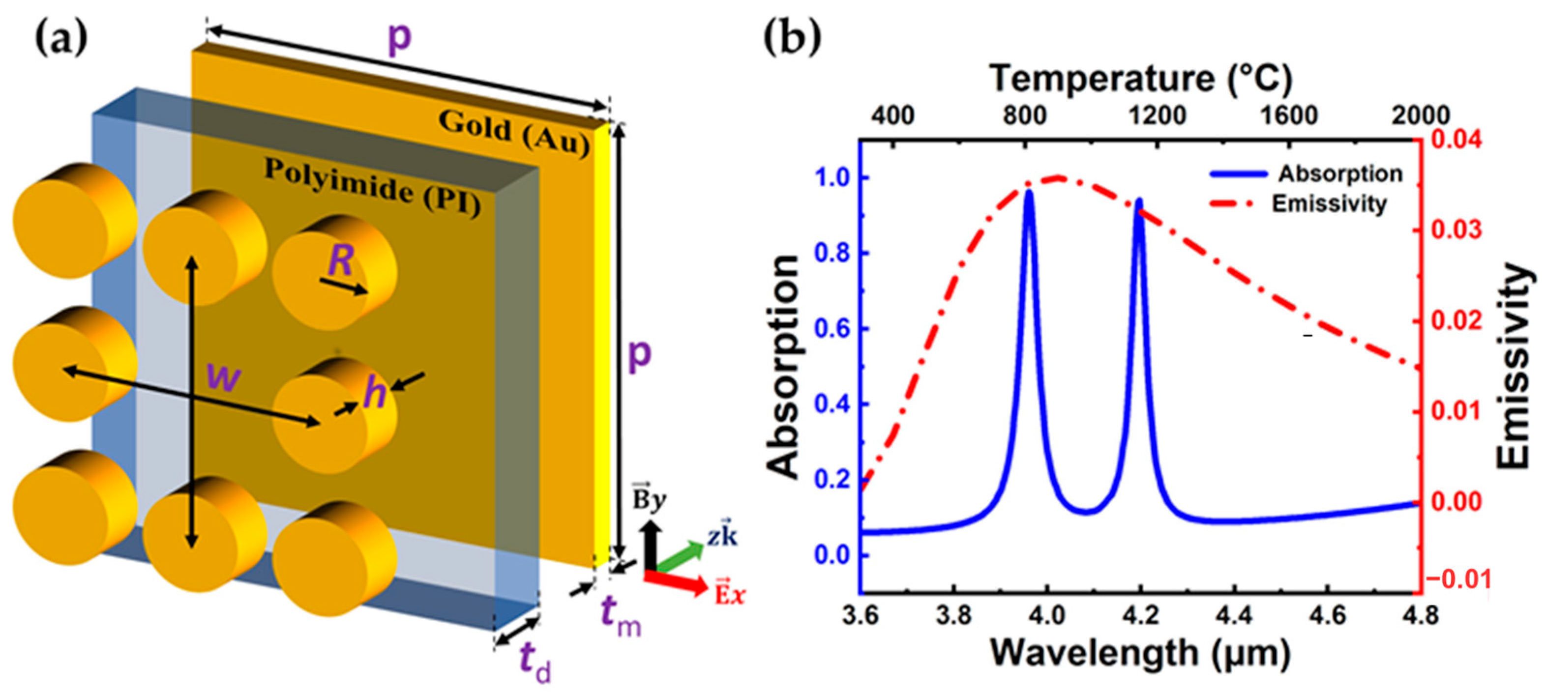
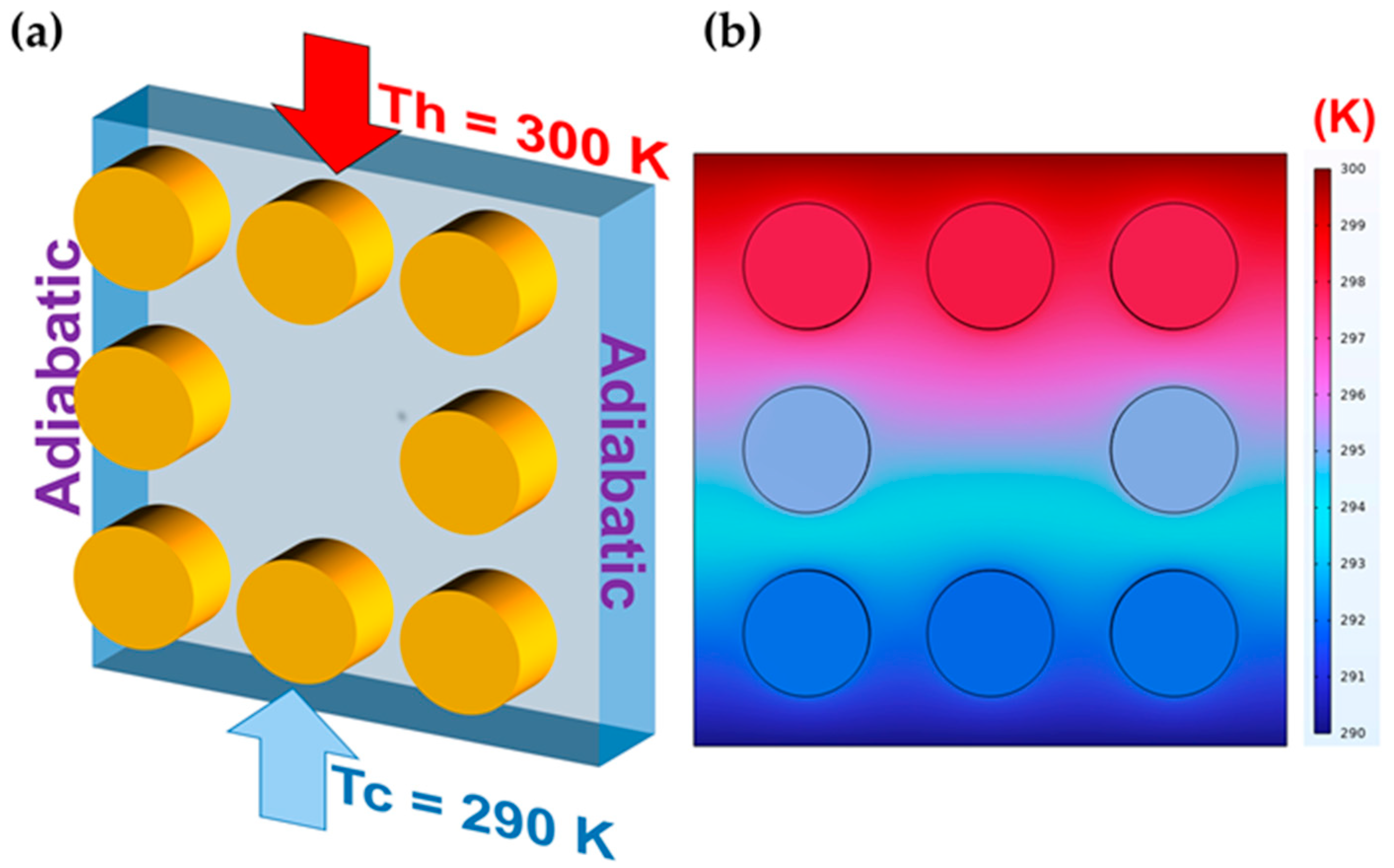
2.1. Metamaterial Design and Its Equivalent Parameters

In our previous work [14], we proposed a novel metasurface structure optimized for IR sensing applications, which is presented in Figure 1a. The proposed MM consisted of three layers: two gold layers separated by a polyimide dielectric material. The dielectric layer thickness (td) of 0.29 μm was found to be optimal in achieving the desired spectral positions and absorptions of two resonance peaks. The central gap (w) of 3.68 μm and disk radius (R) of 0.63 μm were also optimized to enhance the performance. Our simulations used a polyimide permittivity of 3.5 and a loss tangent of 0.0027, with the bottom gold layer having a thickness of 0.1 μm and the top featuring an eight-disk pattern with a disk thickness of 0.19 μm. The unit cell periodicity was set to be 5.96 μm.
Figure 1b illustrates the absorption spectrum of the MM structure (solid line). The optimized MM structure exhibits two prominent absorption peaks at 3960 and 4197 nm, with absorptions of 96.3% and 94.1%, respectively, which are polarization independent [14]. These peaks align well with CO2 absorption wavelengths, making the MM particularly suitable for CO2 sensing applications. This compatibility is crucial since CO2 molecules absorbed wavelengths around 4200 nm, and the common reference wavelength was 3950 nm [13].
The comparative analysis revealed that our MM had a narrower full width at half maximum (FWHM), 38 nm at 4197 nm and 45 nm at 3960 nm, compared to other studies [13,15,16]. This narrower emission band enhanced the spectral selectivity and precision, which are crucial for high sensitivity and accuracy in IR sensing and imaging systems. The improved control on the spectrum provided by the narrower FWHM was transferred to an increased signal-to-noise ratio and improved detection capability. This enhancement means that the signal of interest is amplified while the background noise is minimized, leading to better detection sensitivity and reliability in practical applications.
Furthermore, the reduced FWHM of our MM improved energy efficiency by narrowing the range of emitted radiation to match the desired wavelengths more precisely. To provide clarity, we compared the radiative properties of our MMs with those of the ideal blackbody. According to Kirchhoff’s law, a material’s absorptivity α λ is equal to its emissivity ε ( λ ) under thermal equilibrium conditions [17]. The total emissivity of the metasurface can be evaluated from the following equation by normalizing the radiation of the MM to that of the ideal blackbody [18]:
ε = ε T = E E b = 0 α λ E b λ λ , T d λ σ B T 4 .
where E b denotes the total emissive power of a blackbody, E b λ represents the monochromatic emissive power at a given wavelength λ , and σ B is the Stefan–Bolzman constant.
The red dash–dotted line in Figure 1b depicts the temperature dependence of normalized emissivity. The MMs exhibit promising characteristics for applications requiring the selective emission of IR wavelengths while minimizing energy consumption. With normalized emissivity ε values ranging from 0.14% to 0.35% at various temperatures, these materials are tailored to emit radiation specifically in the desired IR region, crucial for precise IR detection applications. This target emission reduces energy waste associated with emitting extraneous wavelengths, resulting in improved energy efficiency compared to traditional blackbody emitters. Additionally, focused emission contributes to the prolonged operational lifespan of IR detection systems by integrating MM technology.
In this study, we confront the significant challenge of efficiently simulating the integration of MMs with heaters, a task complicated by the computational demands arising from the intricate structures of metasurfaces composed of numerous unit cells. To mitigate this computational burden, we propose a novel strategy in which the top metal layer, composed of gold disks, and the intermediate dielectric layer (polyimide) of MM, are replaced with an equivalent layer characterized by homogeneous parameters. The equivalent thickness, density, and specific heat are calculated by using the following formulas:
t e = β i t i ,
ρ e = β i t i ρ i t e ,
c e = β i ρ i t i c i ρ e t e ,
where β i is the coefficient equal to the ratio of the area of layer i to the whole area of the metasurface, ρ i , t i , and c i are the density, thickness, and thermal capacity at the constant pressure of layer i.
To determine the effective thermal conductivity k e of the entire sheet, we ascertain the thermal conductivity of the stack material region k s by using the following parallel thermal conductivity model [18]:
k s = k i t i t i ,
where k i is the thermal conductivity of layer i. Then the Maxwell–Eucken formula [19,20] was employed to evaluate k e as
k e = k s 2 k s + k d 2 k s k d γ   2 k s + k d + k s k d γ ,
where k d is the thermal conductivity of the dielectric layer and γ is the volume fraction of the stack layer. The effective thermal conductivity derived by this method was found to be 0.23 W/(m·K).
At the same time, utilizing COMSOL Multiphysics software, the finite element simulations were employed to model a representative unit cell. Figure 2a illustrates the boundary conditions, while Figure 2b presents the temperature distribution of the sheet. The effective thermal conductivity was calculated by using the relation,
k s i m = q L T h T c ,
where q represents the heat flux in the unit cell, obtained by integrating the fluxes across the hot or cold surface as follows:
q = 1 A k T d S .
where A denotes the area of the hot or cold surface. The effective thermal conductivity of the simulation was determined to be 0.22 W/(m·K) indicating excellent agreement with the theoretical prediction.

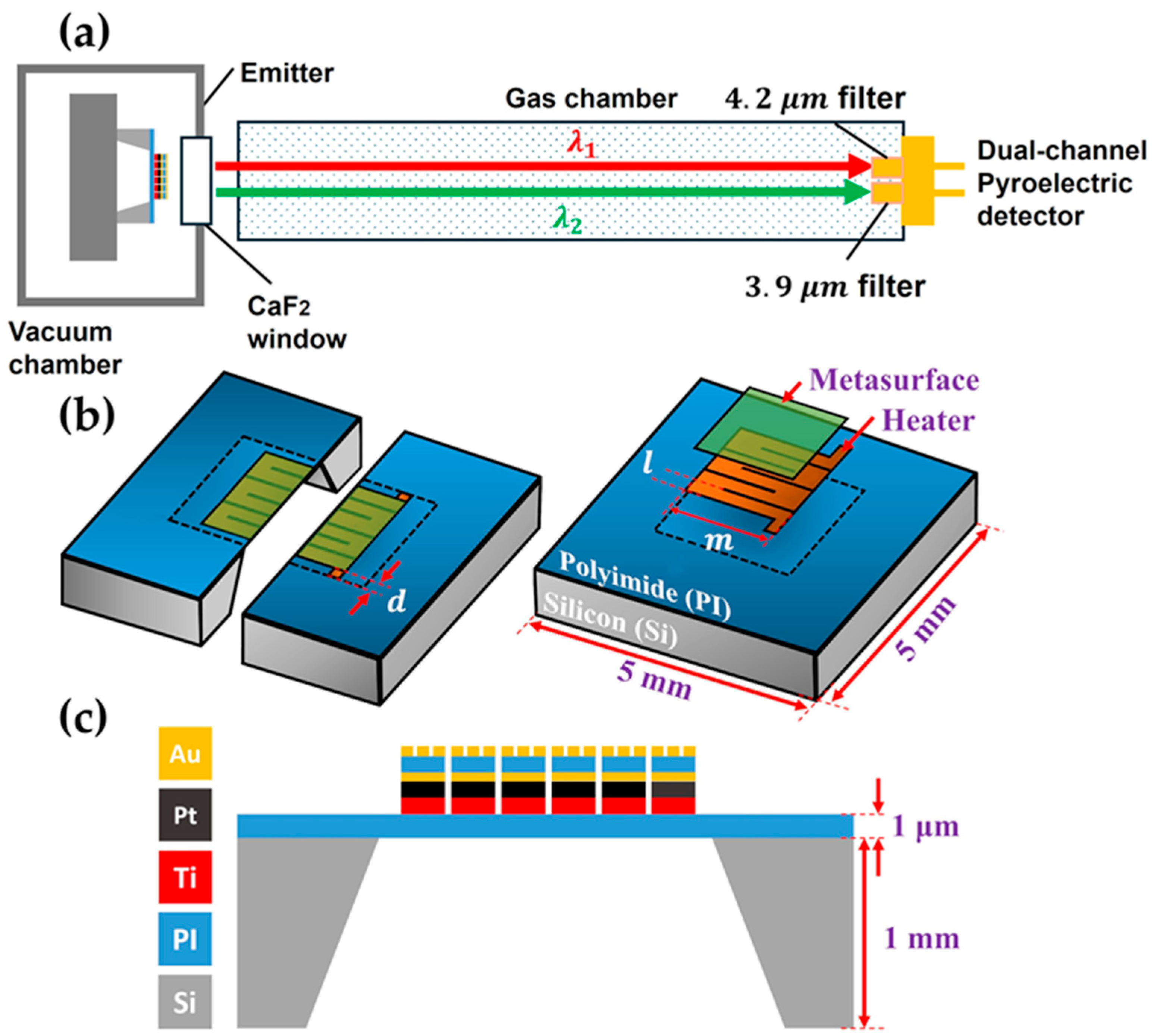
2.2. Metamaterial-Integrated Microheater Design

The sensor configuration, as shown in Figure 3a, is based on a typical non-dispersive IR setup commonly used for gas detection. The system is composed of four main components: the metamaterial-integrated emitter, a gas chamber, wavelength-specific optical filters, and a dual-channel pyroelectric detector [13,21]. The emitter used in this setup is our custom-designed MM-integrated microheater, engineered to emit IR radiation at two narrow spectral bands centered at 4197 and 3950 nm, with narrow FWHM. These wavelengths correspond closely to the absorption peak of carbon dioxide at 4.2 µm and a nearby reference wavelength that is not absorbed by gases.
The use of a metasurface enabled highly spectrally selective emission, significantly reducing the radiative energy wasted at off-target wavelengths and improving the energy efficiency of the sensor. After passing through the gas chamber, the IR beam was split into two optical paths by a set of narrowband filters. A 4.2 µm filter allowed only radiation at λ1 (gas absorption band) to reach one channel of the detector, while a 3.9 µm filter allowed radiation at λ2 (reference band) to reach the second channel. This dual-channel detection enabled differential measurement to compensate for background radiation, thermal drift, and optical noise.
The schematic diagram of our metamaterial-integrated microheater is presented in Figure 3b,c. The substrate of the microheater was made of 1-mm-thick silicon (Si). A suspended membrane with dimensions of 5 mm × 5 mm and a thickness of 1 μm was fabricated from polyimide due to its robustness, low thermal conductivity, and ease of fabrication. Polyimide was chosen because its thermal expansion coefficient closely matched that of Si, making it highly compatible with integrated-circuit fabrication processes [22].
The heating element consisted of a meander-shaped heater made of titanium (Ti) and platinum (Pt). Ti served as an adhesive layer while Pt, being chemically inert and having a good thermal response to low voltage, was chosen for its linear resistivity–temperature relationship and excellent long-term stability. Additionally, the bottom gold (Au) layer functioned as both a heater and a back reflector, enhancing the IR emission efficiency by reducing the distance between the meanders to 4 μm. The metal linewidth of the heater was l = 0.33   m m and its length was m = 2   m m . The layer configuration is illustrated in Figure 3c.
The device was simulated in vacuum conditions to eliminate the convection losses. Upon the application of power to the heater, the thermal equilibrium was swiftly obtained within the suspended polyimide membrane. Heat transfer primarily occurred through conduction and radiation mechanisms.
In this investigation, COMSOL Multiphysics 6.2 was employed for finite element modeling and heat distribution simulation. To alleviate computational complexity, the top metal layer comprising Au disks and the intermediate polyimide dielectric layer in the MM were substituted with a homogeneous layer characterized by equivalent parameters in Section 2.1. For clarity and reproducibility, the material properties used in both electromagnetic and thermal simulations are summarized in Table 1.
The emitter device can be fabricated by using a standard MEMS-compatible process similar to those previously demonstrated for suspended microheater structures [13,27]. The process began with a Si substrate on which an adhesion promoter was applied, followed by the spin-coating of a polyimide layer (e.g., PI-2575). This polyimide was cured in a nitrogen environment at elevated temperatures (typically 360–400 °C) to form a uniform insulating membrane [27]. A Ti/Pt/Au metal stack was then deposited and patterned via photolithography and lift-off to form a meander-shaped microheater, where Ti enhanced adhesion, Pt served as the resistive heating element, and Au improved conductivity and IR reflectivity. A second polyimide layer was then deposited. To provide access to the heater terminals, the polyimide above the contact pads was selectively removed by using photolithography followed by oxygen plasma etching. The metasurface, consisting of subwavelength Au structures, was patterned by electron-beam lithography [13]. Finally, the Si substrate was etched from the backside by using anisotropic wet etching in KOH (8 mol/L at ~92 °C) to release the suspended membrane.

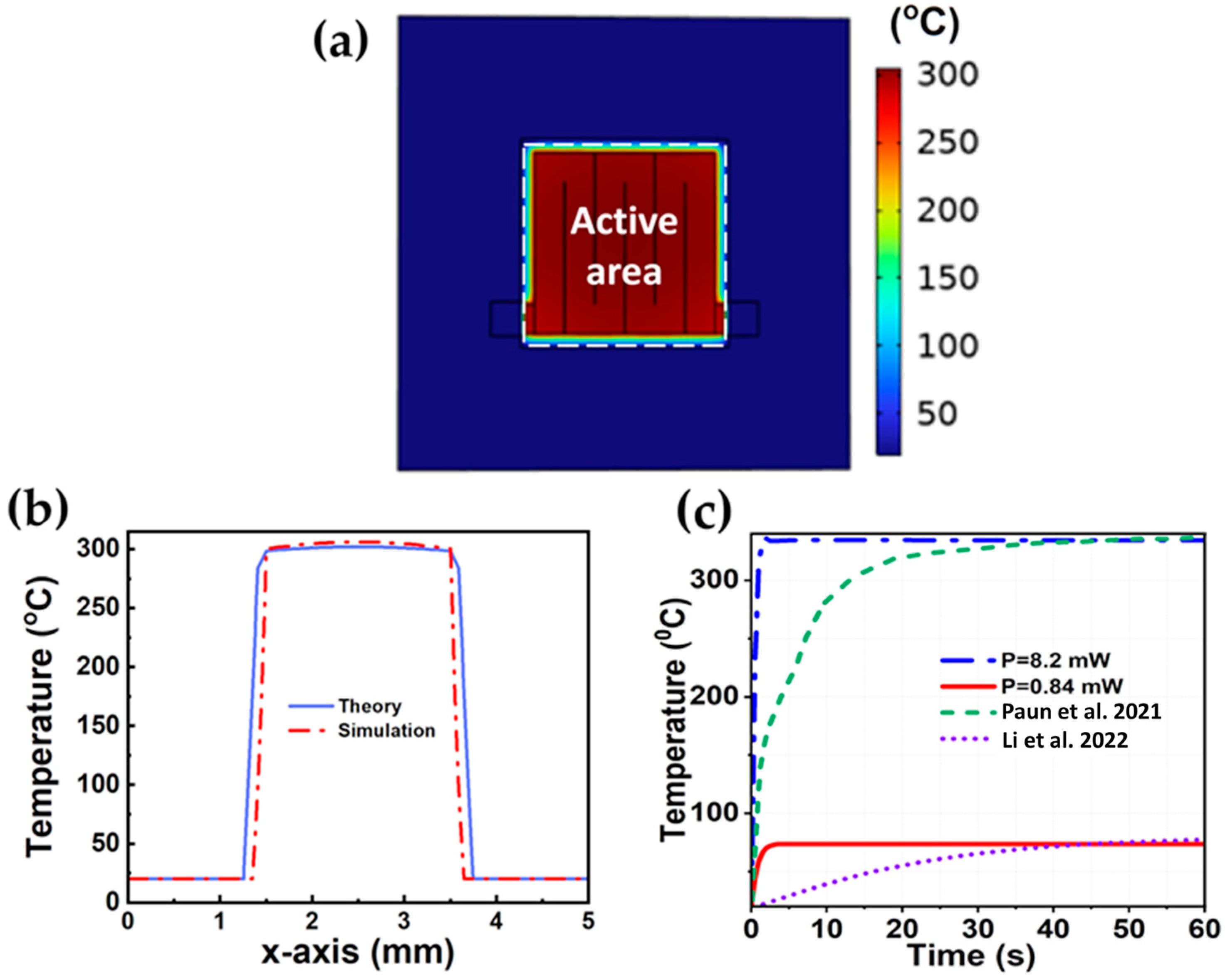
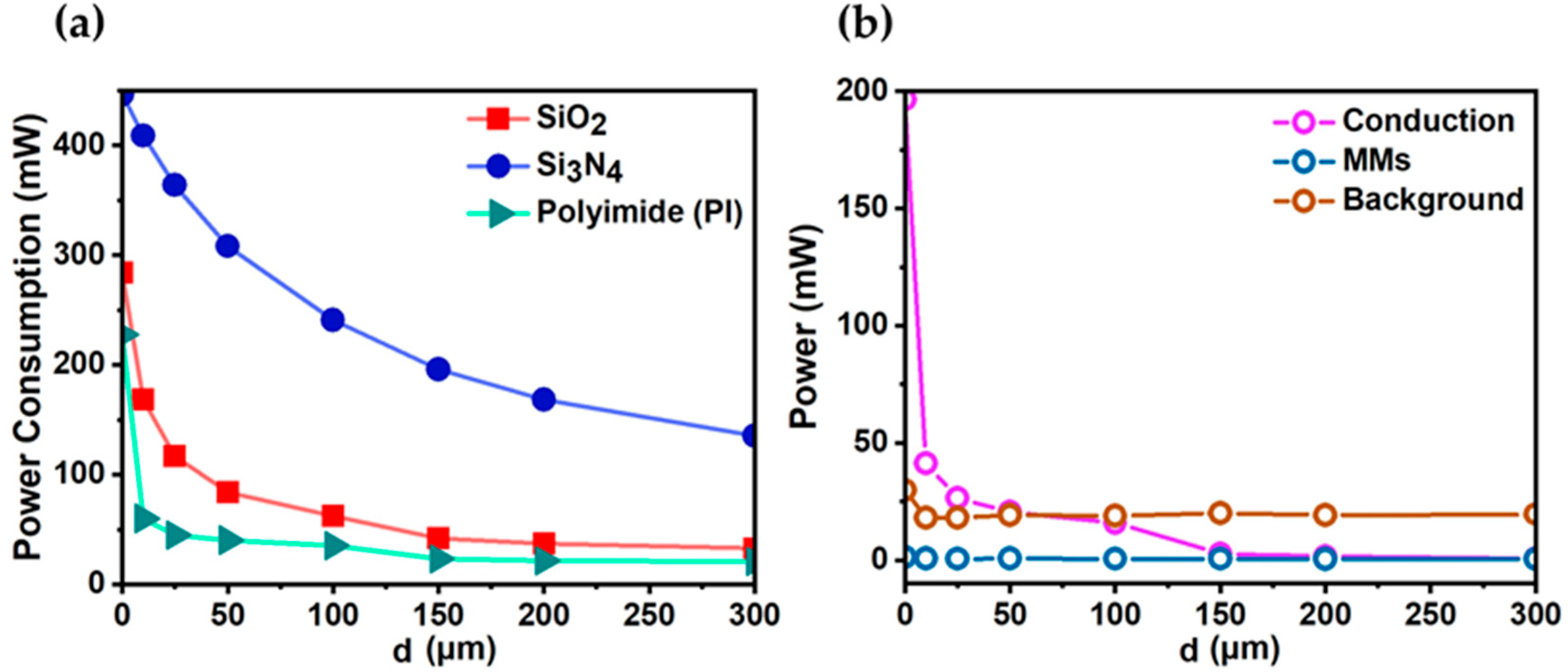
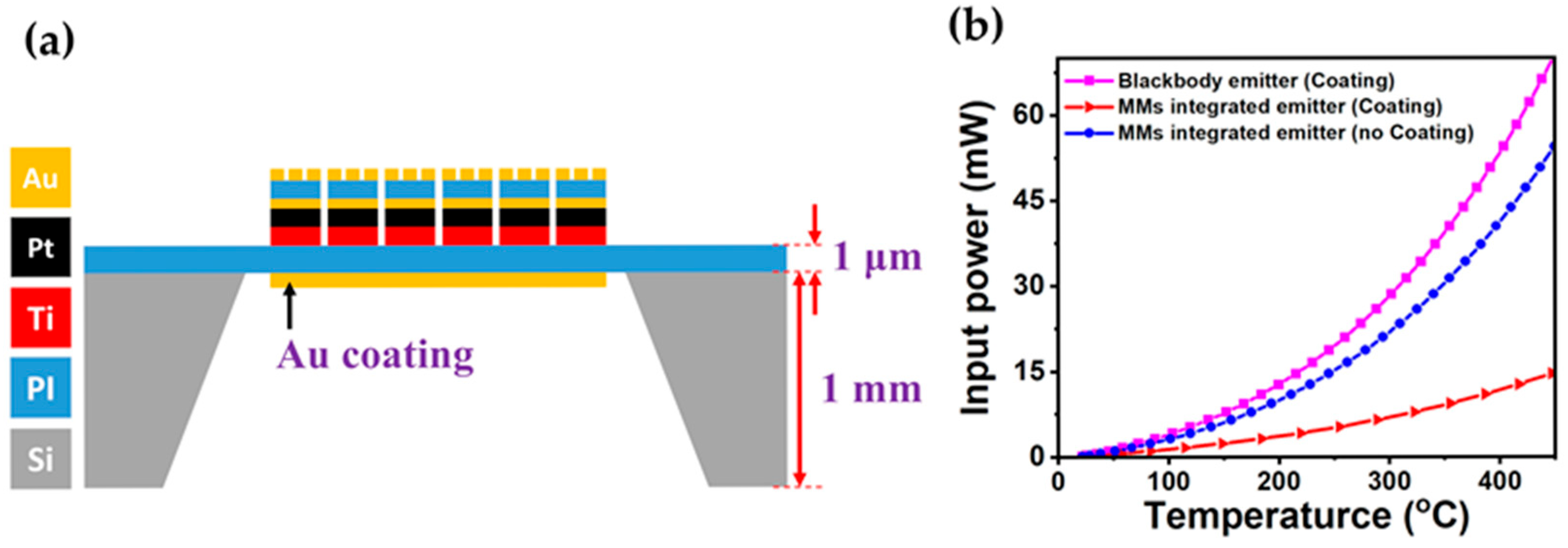
3. Results and Discussion

In IR emitters, power loss can be primarily attributed to two mechanisms: radiation loss and conduction loss along the membrane. Understanding these mechanisms and implementing strategies to mitigate them are essential in improving the energy efficiency of IR devices.
The conduction loss within the membrane can be approximated by using a simplified formula derived for a circular membrane [28,29] to be
P c = 2 π k t Δ T l n   r a r i .
where, t represents the membrane thickness, k represents the thermal conductivity of the membrane, r i and r a correspond to the radii of the heated and membrane areas, respectively, and Δ T signifies the temperature difference between the heated region and the ambient environment. Equation (9) highlights that minimizing the thermal conduction loss entails selecting a membrane material with a low thermal conductivity. In our proposed design, polyimide was chosen owing to its favorable combination of low thermal conductivity and straightforward fabrication process.
Figure 4a illustrates the simulated power consumption as a function of the distance d between the heated region and the Si rim for various materials, with an average temperature in the active area remaining at 300 °C. Notably, polyimide demonstrates the lowest power consumption compared to silicon dioxide or silicon nitride membranes, due to its inherently low thermal conductivity. Specifically, at a d of 150 μm, the power consumption for polyimide stands at 18.7 mW. In contrast, silicon dioxide exhibits a power consumption of 42 mW, while silicon nitride indicates the highest power consumption of 196 mW, primarily due to its high thermal conductivity, which is approximately 133 times greater than that of polyimide.
Figure 4b demonstrates that conduction loss significantly affects overall power consumption, particularly at shorter distances between the heated area and the Si rim. Conduction loss decreases as d increases, highlighting the importance of thermal isolation in minimizing power consumption. At a d of 150 μm, the conduction loss is reduced to only 2.6 mW, a marked reduction from the higher losses observed at shorter distances. However, it is noted that increasing the distance beyond 150 μm does not significantly enhance the thermal isolation further, indicating a threshold beyond which the conduction loss is stabilized. This suggests that optimizing the distance to around 150 μm is crucial in achieving efficient thermal management with minimal conduction loss.
In addition to managing the conduction loss, control of the radiation loss is equally important in minimizing power consumption. Radiation loss, which includes background radiation loss and metasurface emission power, remains relatively constant regardless of distance d. When d = 150 μm, the background radiation loss is substantial at 18.7 mW, while the radiated power of the metasurface is considerably lower: 0.5 mW. The metasurface design ensures that it emits radiation selectively, focusing the energy where it is needed and minimizing unnecessary losses, thereby enhancing the overall energy efficiency of the system. The background radiation loss, being the dominant form of loss, surpasses both conduction loss and radiated power by the metasurface at this distance. To mitigate the radiation loss, a 50 nm layer of Au was applied to the back of the polyimide base in the heated area, as shown in Figure 5a. Au, with its high reflectivity, effectively reduced the radiation loss by reflecting thermal radiation back into the system, thus lowering the overall power consumption. Additionally, the metasurface is engineered to emit power efficiently, reducing the energy consumption compared to the blackbody emitter.
To effectively demonstrate the advantages of integrating metasurfaces with emitters and coatings, we analyzed and compared the performance data of different emitters: the metamaterial-integrated emitter without a coating, the blackbody emitter with a coating, and the metamaterial-integrated emitter with a coating. The blackbody emitter was made by applying the blackbody paint with an emittance of 0.94 on the membrane heater of the equivalent metasurface emitter instead of the metasurface pattern. Figure 5b illustrates the power consumption characteristics of three different types of emitters across an average temperature range. The power consumption of the blackbody emitter is the highest among the three types across all temperatures. This is because a blackbody emitter emits radiation in a broad spectrum, leading to significant energy loss despite the reflective coating. The metasurface-integrated emitter with coating, combined the selective emission properties of the metasurface with a gold-coated polyimide base. This emitter exhibits the lowest power consumption. The metasurface efficiently directed the emitted radiation, significantly reducing the power loss. The Au coating further enhanced efficiency by reflecting thermal radiation back into the system. This synergistic effect results in superior energy conservation, making it the most efficient emitter in terms of power consumption. The metasurface-integrated emitter without coating employed the metasurface for selective emission but lacked the Au coating. While more efficient than the blackbody emitter, this type of emitter consumed more power than the metasurface emitter with coating. The absence of the reflective Au layer means that some thermal radiation is not reflected into the system, leading to higher power consumption compared to the coated version.
Table 2 compares the power consumption of these devices and that in Ref. [13] when their average temperature was 300 °C. The data highlights the significant advantages of the use of a metasurface with a Au coating. The addition of this coating reduces the background radiation from 18.7 to 4.0 mW, resulting in a substantial decrease in overall power consumption. This demonstrates that the coating is highly favorable for improving the efficiency of the emitter. The blackbody emitter, despite the coating, consumes more power and emits a broad spectrum of radiation, leading to higher energy loss. By utilizing the metasurface emitter, the required power is reduced by 76% at an average temperature of 300 °C. This significant power saving is attributed to the selective emission properties of the metasurface. The proposed emitter (MM-integrated emitter with coating) significantly outperforms that in Ref. [13], since the emission power at 300 °C of our emitter is approximately 0.5 mW, six times lower than the 3 mW in Ref. [13]. Overall, at 300 °C our emitter uses 6.8 mW, which is eight times lower than the reported value of 58 mW in Ref. [13]. This indicates the superior efficiency of our design in reducing both conduction and radiation losses, making it a highly effective solution for thermal management.
Figure 6a illustrates the surface temperature distribution of the MM-integrated emitter with a coating when the average temperature within the active area was 300 °C. The temperature was observed to be uniformly distributed within the active area, rapidly decreasing to the ambient temperature at the edge of the membrane. To better understand the heat flow within and from the structure, a simplified model was developed by approximating the square membrane with a circular one [29,30]. The radius of the circle was selected to minimize the area of non-overlap between the square and the circle, as described in Ref. [30]. Specifically, the radius was 0.5412a, where a represents the side length of the square. Considering that radiation loss was significant within the active area and negligible in other regions owing to lower temperatures, we accounted for the radiation loss solely within the active area. We linearized the heat flux at T = T a , where T a is the average temperature within this active region, to be [14]
q r a d = ε σ B T 4 T 0 4 = γ ( T T * ) ,
γ = 4 σ B ε T 0 3 ,   a n d   T * = 3 T a 4 + T 0 4 4 T a 3 ,
where σ B is the Stefan–Bolzman constant.
The heat transfer equations are simplified to be the one-dimensional problem as in our previous work [14]:
d 2 T d r 2 + 1 r d T d r γ k t T T * σ γ = 0 ,
where t represents the effective thickness of the active region, determined by using Equation (2) above and σ is the heating power density. Parameter k denotes the effective thermal conductivity of the active region. Initially, we replaced the top two layers of the MM structure with an equivalent layer based on the Maxwell–Eucken model, as described in Section 2.1. Subsequently, the effective thermal conductivity of the entire active region was determined as follows [31]:
k = α i k i t i t ,
where α i is the coefficient equal to the ratio of the area for layer i to the whole area of the active region.
The temperature of the edge substrate was set to be the same as the ambient temperate T 0 (the Dirichlet boundary condition). The solution in the inner region is as follows [14]:
T 1 r = T * + P γ e π r 0 t + A I 0 n 0 r + B K 0 n 0 r ,
where n 0 = γ e / k t . I 0 and K 0 represent the zeroth-order modified Bessel functions of the first and second kinds, respectively.
Figure 6. (a) Surface temperature distribution of emitters with coating. (b) Temperature distribution along x axis. (c) Comparison of the thermal transient response of the proposed model with those in Refs. [32,33].
Photonics 12 00583 g006
The heat equation in the outer region is given by d d r r d T = 0 . The solution is
T 2 r = C l n r + D .
The boundary conditions are T 1 0 = 0 ,
T 2 r a = T 0 ,
T 1 r 0 = T 2 r 0 ,
k 1 T 1 r 0 = k 2 T 2 r 0 .
The four unknown constants A, B, C, and D can be determined by solving these equations. Our solutions include the average temperature of the hot region T a as the input data. From expression (11) we calculate the average temperature in the heating region and set it to be equal to the input value T a . From there, we obtain the relationship between the average temperature T a and the input power as follows:
T 1 0 + T 1 r 0 2 = T a .
Equation (12) is a first-order linear equation with the unknown being the input power P . By solving this, we obtained the required input power P .
According to the theoretical model, the input power required for the active region of the emitter to achieve an average temperature of 300 °C was 4.5 mW, which is of the same order of magnitude as the simulation result of 6.8 mW in Table 2 above. This discrepancy arose because the theoretical model simplified the calculation process by neglecting emissions in the outer region. Figure 6b displays the temperature distribution along the x-axis as calculated by the theoretical model (solid line), together with that obtained from the simulation (dash–dot line). The results show good agreement, indicating the validity of the theoretical approach despite the simplifications.
A transient thermal analysis using COMSOL Multiphysics provided insights into the thermal behavior of IR emitters, particularly their response time to reach the steady-state temperature after a change in input power. As illustrated in Figure 6c, the temperature of a coated emitter increases with rising input power, reaching thermal equilibrium in 2 s. In comparison, the microheater reported in Ref. [32] required approximately 20 s, while that in Ref. [33] took 60 s to reach thermal equilibrium. This demonstrates the significantly faster thermal response of the IR emitter in this study. The improved response time is attributed to a decrease in radiation losses due to the application of MM and coating, a reduction in convection losses by placing the emitter in the vacuum environment and the minimization of conduction losses due to the low thermal conductivity of polyimide. As a result, the input power was used more efficiently for heating, allowing for the faster achievement of the target temperature and steady state.

4. Conclusions

This study has presented an innovative approach to simulating and optimizing the integration of MMs with microheaters. By replacing complex MM structures with equivalent homogeneous layers for simulations, we effectively reduced associated computational demands. Our findings revealed that polyimide, due to its low thermal conductivity, significantly lowered power consumption compared to other materials such as silicon dioxide and silicon nitride.
The application of Au coating to the MM further enhanced energy efficiency by reducing losses. The comparative analysis indicated that the metasurface-integrated emitter with Au coating outperformed other emitter designs, achieving substantial power savings and improved temperature uniformity. This highlights the effectiveness of combining the metasurface with thermal management techniques to develop highly efficient emitters.
Our proposed emitter design showed a significant reduction in power consumption, requiring only 6.8 mW to achieve a temperature of 300 °C, while maintaining temperature uniformity and a relatively fast response time. This significant improvement was attributed to the selective emission properties of the metasurface and the optimization of conduction and radiation losses. The results underscore the potential of metasurface-based emitters for advanced energy-efficient applications, offering a promising solution to the challenges associated with thermal management in various technologies.

Author Contributions

Conceptualization, Y.L. and B.X.K.; methodology, P.D.T. (Pham Dinh Tuan), L.C., N.P.H., N.P.V. and B.S.T.; validation, B.X.K., H.T.G., V.D.L., L.C. and Y.L.; investigation, N.H.A., D.K.T., N.T.T. and D.X.P.; writing—original draft preparation, P.D.T. (Pham Duy Tan); writing—review and editing, V.D.L. and Y.L.; supervision, Y.L. All the authors discussed and commented on the manuscript. All authors have read and agreed to the published version of the manuscript.

Funding

This research was supported by the Vietnam Ministry of Science and Technology through the national-level project ĐTĐLCN.18/23, and by the Shanghai Science and Technology Commission under grant #24110714600.

Institutional Review Board Statement

Not applicable.

Informed Consent Statement

Not applicable.

Data Availability Statement

The data used and/or analyzed during the current study are available from the corresponding author upon reasonable request.

Conflicts of Interest

The authors declare no conflicts of interest.

References

  1. Stanley, R. Plasmonics in the mid-infrared. Nat. Photonics 2012, 6, 409–411. [Google Scholar] [CrossRef]
  2. Kumar, P.; Morawska, L.; Martani, C.; Biskos, G.; Neophytou, M.; Di Sabatino, S.; Bell, M.; Norford, L.; Britter, R. The rise of low-cost sensing for managing air pollution in cities. Environ. Int. 2015, 75, 199–205. [Google Scholar] [CrossRef] [PubMed]
  3. Hodgkinson, J.; Tatam, R.P. Optical gas sensing: A review. Meas. Sci. Technol. 2013, 24, 012004. [Google Scholar] [CrossRef]
  4. Nguyen, H.A.; Pham, T.S.; Tung, B.S.; Khuyen, B.X.; Le, D.T.; Vu, H.Y.; Vu, D.L.; Hien, N.T. Metamaterials based on hyperbolic-graphene composite: A pathway from positive to negative refractive index at terahertz. Comput. Mater. Sci. 2025, 248, 113574. [Google Scholar] [CrossRef]
  5. Fan, K.; Averitt, R.D.; Padilla, W.J. Active and tunable nanophotonic metamaterials. Nanophotonics 2022, 11, 3769–3803. [Google Scholar] [CrossRef]
  6. Li, M.; Xu, H.; Yang, X.; Xu, H.; Liu, P.; He, L.; Nie, G.; Dong, Y.; Chen, Z. Tunable plasma-induced transparency of a novel graphene-based metamaterial. Results Phys. 2023, 52, 106798. [Google Scholar] [CrossRef]
  7. Ou, H.; Lu, F.; Xu, Z.; Lin, Y.-S. Terahertz metamaterial with multiple resonances for biosensing application. Nanomaterials 2020, 10, 1038. [Google Scholar] [CrossRef]
  8. Do, T.C.; Khuyen, B.X.; Tung, B.S.; Viet, N.N.; Ha, D.T.; Hanh, V.T.H.; Do, X.P.; Tung, D.K.; Nguyen, H.A.; Lam, V.D. Wide-angle electromagnetic wave absorption via multilayer metamaterial structures. Phys. Scr. 2025, 100, 025538. [Google Scholar] [CrossRef]
  9. Qu, Y.; Chen, Y.; Chen, S.; Wu, Q.; Liu, J.; Yi, Z.; Fu, L. Research on Multi-Resonance Mechanism to Achieve Ultra-Wideband High Absorption of a Metamaterial Absorber in the UV to MIR Range. Chin. J. Phys. 2024, 91, 632–643. [Google Scholar] [CrossRef]
  10. Chen, Y.; Liang, J.; Chen, S.; Yi, Z.; Fu, L.; Yang, W. Bi-Directional High-Performance Metamaterial Perfect Absorber for Solar Harvesting and Refractive Index Sensing. Mater. Today Nano 2024, 26, 100487. [Google Scholar] [CrossRef]
  11. Bhati, R.; Malik, A.K. Multiband terahertz metamaterial perfect absorber for microorganisms detection. Sci. Rep. 2023, 13, 19685. [Google Scholar] [CrossRef] [PubMed]
  12. Gao, W.; Chen, F.; Yang, W. Temperature and refractive index sensor based on perfect absorber in InSb double rectangular ring resonator metamaterials. Mater. Today Commun. 2024, 40, 109461. [Google Scholar] [CrossRef]
  13. Miyazaki, H.T.; Kasaya, T.; Iwanaga, M.; Choi, B.; Sugimoto, Y.; Sakoda, K. Dual- band infrared metasurface thermal emitter for CO2 sensing. Appl. Phys. Lett. 2014, 105, 121107. [Google Scholar] [CrossRef]
  14. Khuyen, B.X.; Ngoc, N.V.; Dung, D.N.; Hai, N.P.; Tung, N.T.; Tung, B.S.; Lam, V.D.; Giang, H.T.; Tan, P.D.; Chen, L.; et al. Dual-band infrared metamaterial perfect absorber for narrow-band thermal emitters. J. Phys. D Appl. Phys. 2024, 57, 285501. [Google Scholar] [CrossRef]
  15. Mihai, L.; Mihalcea, R.; Tomescu, R.; Paun, C.; Cristea, D. Selective mid-IR metamaterial-based gas sensor system: Proof of concept and performances tests. Nanomaterials 2022, 12, 1009. [Google Scholar] [CrossRef] [PubMed]
  16. Xu, R.; Lin, Y.-S. Tunable infrared metamaterial emitter for gas sensing application. Nanomaterials 2020, 10, 1442. [Google Scholar] [CrossRef]
  17. Li, Y.; Li, W.; Han, T.; Zheng, X.; Li, J.; Li, B.; Fan, S.; Qiu, C.W. Transforming heat transfer with thermal metamaterials and devices. Nat. Rev. Mater. 2021, 6, 488–507. [Google Scholar] [CrossRef]
  18. Pitts, D.; Sissom, L.E. Schaum’s Outline of Heat Transfer, 2nd ed.; McGraw Hill: New York, NY, USA, 2011. [Google Scholar]
  19. Wang, J.; Carson, J.K.; North, M.F.; Cleland, D.J. A new structural model of effective thermal conductivity for heterogeneous materials with co-continuous phases. Int. J. Heat Mass Transf. 2008, 51, 2389–2397. [Google Scholar] [CrossRef]
  20. Xue, Q. Model for effective thermal conductivity of nanofluids. Phys. Lett. A 2003, 307, 313–317. [Google Scholar] [CrossRef]
  21. Jia, X.; Roels, J.; Baets, R.; Roelkens, G. On-chip non-dispersive infrared CO2 sensor based on an integrating cylinder. Sensors 2019, 19, 426. [Google Scholar] [CrossRef]
  22. Yu, S.; Wang, S.; Lu, M.; Zuo, L. A novel polyimide based micro heater with high temperature uniformity. Sens. Actuators A Phys. 2017, 257, 58–64. [Google Scholar] [CrossRef]
  23. Sanowitz, S. Radiative Properties of Silicon Related Materials. Master’s Thesis, New Jersey Institute of Technology, Newark, NJ, USA, 31 May 2016. [Google Scholar]
  24. Okada, T.; Ishige, R.; Ando, S. Analysis of thermal radiation properties of polyimide and polymeric materials based on ATR-IR spectroscopy. J. Photopolym. Sci. Technol. 2016, 29, 251–254. [Google Scholar] [CrossRef]
  25. Raghu, O.; Philip, J. Thermal properties of paint coatings on different backings using a scanning photo acoustic technique. Meas. Sci. Technol. 2006, 17, 2945. [Google Scholar] [CrossRef]
  26. Dewitt, D.P.; Bergman, T.L.; Lavine, A.S. Fundamentals of Heat and Mass Transfer, 6th ed.; John Wiley: New York, NY, USA, 2006. [Google Scholar]
  27. Aslam, M.; Gregory, C.; Hatfield, J.V. Polyimide membrane for micro-heated gas sensor array. Sens. Actuators B 2004, 103, 153–157. [Google Scholar] [CrossRef]
  28. Dibbern, U. A substrate for thin-film gas sensors in microelectronic technology. Sens. Actuators B Chem. 1990, 2, 63–70. [Google Scholar] [CrossRef]
  29. Simon, I.; Bârsan, N.; Bauer, M.; Weimar, U. Micromachined metal oxide gas sensors: Opportunities to improve sensor performance. Sens. Actuators B Chem. 2001, 73, 1–2. [Google Scholar] [CrossRef]
  30. Bhattacharyya, P.; Sen, S.; Chatterjee, A.; Saha, H. Design of the optimum microheater for smart MEMS gas sensor. In Proceedings of the ISSS 2005 International Conference on Smart Materials Structures and Systems, Bangalore, India, 28–30 July 2005. [Google Scholar]
  31. Kozlov, A.G. Analytical modelling of steady-state temperature distribution in thermal microsensors using Fourier method: Part 1. Theory. Sens. Actuators A Phys. 2002, 101, 283–298. [Google Scholar] [CrossRef]
  32. Paun, C.; Tomescu, R.; Parvulescu, C.; Ionescu, O.; Gavrila, D.E.; Cristea, D. Microheater optimized for the integration with metasurface-based IR sources for gas sensing application. Rom. J. Inf. Sci. Technol. 2021, 24, 201–212. [Google Scholar]
  33. Li, D.; Ruan, Y.; Chen, C.; He, W.; Chi, C.; Lin, Q. Design and thermal analysis of flexible microheaters. Micromachines 2022, 13, 1037. [Google Scholar] [CrossRef]
Figure 1. (a) Schematic of the proposed MM. (b) Dual-band absorption spectrum (in blue), and temperature dependence of the normalized emissivity (in red).
Photonics 12 00583 g001
Figure 2. (a) Boundary conditions. (b) Temperature distribution of the unit cell.
Photonics 12 00583 g002
Figure 3. (a) Sensor configuration. Structure of the MM-integrated IR microheater: (b) top view; (c) cross-sectional view.
Photonics 12 00583 g003
Figure 4. (a) Dependence of power consumption on distance d with an average temperature in the active area maintained at 300 °C. (b) Conduction loss, metasurface emission, and background radiation as functions of distance d.
Photonics 12 00583 g004
Figure 5. (a) Cross-sectional view of the emitter with Au coating. (b) Input power vs. average temperature of various emitters.
Photonics 12 00583 g005
Table 1. Material properties.
MaterialThermal Conductivity
(W/mK)
Electrical Conductivity
(S/m)
Density
(kg/m3)
Heat Capacity at Constant Pressure
(J/kg/K)
Emissivity
SiO21.3810−1422007300.7 [23]
Si3N420031007000.7 [23]
Polyimide0.150130011000.7 [24]
Paint 1.450133151840.94 [25]
Au31745.6 × 10619,3001290.05 [26]
Ag42961.6 × 10610,5002350.05 [26]
Table 2. Qualities of recent devices: a comparative evaluation.
DeviceInput Power(mW)Emission Power
(mW)
Background Radiation
(mW)
Conduction
Loss
(mW)
MM-integrated emitter with coating6.80.54.02.3
MM-integrated emitter without coating21.80.518.72.6
Blackbody emitter with coating28.621.64.22.8
Device in Ref. [13]583--
Disclaimer/Publisher’s Note: The statements, opinions and data contained in all publications are solely those of the individual author(s) and contributor(s) and not of MDPI and/or the editor(s). MDPI and/or the editor(s) disclaim responsibility for any injury to people or property resulting from any ideas, methods, instructions or products referred to in the content.

