Abstract
The dispersion relationship of plasmons can be modulated by changing the carrier density of the propagating medium, which provides a new degree of freedom for optical modulation. Traditional graphene plasmonic modulators based on carrier control mainly revolve around chemical doping or voltage control methods, but using a single method of modulation limits the optimization of modulation depth. Herein, we propose a hybrid substrate–dielectric–silicon–graphene structure, which can achieve periodic control of the carrier density in graphene through chemical doping of silicon gratings and overall control of the carrier density by applying an external voltage between the substrate and graphene. The numerical results show that the optical transmission can reach 54.6 dB when the grating length, width, period, and working wavelength are 54 nm, 30 nm, 60 nm, and 8 μm, respectively. The modulation depth of the modulator is significantly optimized by combining the above control mechanisms. This structure will have potential applications in optoelectronic sensing, optoelectronic detection, and optical modulation.
1. Introduction
Surface plasmon polaritons (SPPs) are modes formed by the collective oscillation coupling of light waves with free electrons in metals or doped semiconductors, and their propagation characteristics are highly dependent on the distribution of the carrier density of the propagating medium [1,2,3,4]. Traditional plasmonic components often use metal materials such as gold and silver, but their electron concentrations are limited by the intrinsic properties of the material and are difficult to control dynamically [5,6]. In recent years, active plasmonic materials, such as transparent conductive oxides and two-dimensional materials, have gradually emerged. Their carrier densities can be dynamically adjusted through external fields, such as electric fields, optical fields, or chemical doping, to achieve effective modulation of plasmonic modes [7,8,9,10]. These advances indicate that changing the dispersion relationship of plasmons through controlling the distribution of carrier density can provide a new degree of freedom for the design of optical modulators [11,12,13,14].
Graphene is a promising material in photonic and optoelectronic applications due to its superiority in terms of high carrier mobility, broadband optical response, and facile electrical tunability. It has been reported that highly doped graphene can support SPPs with stronger mode confinement and lower propagation losses compared to noble metals [15,16]. Modulating the propagating SPPs by controlling carrier density distribution in graphene is an effective way to enhance the light–matter interaction and improve the modulation depth [17,18]. There are two common methods to control the distribution of carrier density in graphene: chemical doping and voltage modulation. Chemical doping has high stability and process compatibility [19,20]. For example, Wang Yueke’s group designed a silicon cylinder array that achieved control of the effective refractive index on the surface of graphene via chemical doping [21]. In comparison, voltage modulation has high dynamic response characteristics [22,23]. For instance, our group proposed a multi-parameter tunable plasmonic modulator by dynamically controlling the overall distribution of carrier density in graphene, which achieves the modulation of amplitude, wavelength, and phase simultaneously. However, traditional methods usually use a single method to modulate the distribution of carrier density. Our group reported a related plasmonic modulator by means of controlling the spatial and overall distribution of carrier density, achieving modulation depths of 18.6 dB and 32.7 dB, respectively [24,25]. Unfortunately, the modulation depth has significant potential for improvement. Combining the above control mechanisms could further enhance the performance of plasmonic modulators, enabling high stability and dynamical controllability.
Herein, we propose a hybrid substrate–dielectric–silicon–graphene structure to improve modulation depth. On the one hand, the distribution of carrier density on the graphene surface is modulated by the silicon grating, resulting in a periodic spatial distribution. On the other hand, the overall carrier density distribution of graphene can be altered by applying a voltage between the substrate and graphene. This dual-control mechanism effectively optimizes modulation depth and holds great potential for application in optoelectronic sensing, optoelectronic detection, and optical modulation [26,27,28,29].
2. Model Analysis
2.1. Three-Dimensional Model
The substrate–dielectric–silicon–graphene structure we designed is shown in Figure 1. Graphene was chosen as the propagating medium of the SPPs owing to its fast carrier mobility and voltage controllability. Calcium fluoride (CaF2) was selected as the dielectric layer due to its excellent dielectric properties, while silicon gratings were embedded on the lower surface of the graphene to change the distribution of carrier density. On the one hand, the carrier density in the graphene exhibits a periodic distribution due to the chemical doping effects of silicon grating. On the other hand, the overall carrier density in the graphene can be modulated by applying a voltage between the graphene and substrate. The ability to control the distribution of carrier density can be significantly improved through combining these two control mechanisms, which can significantly improve the modulation depth.
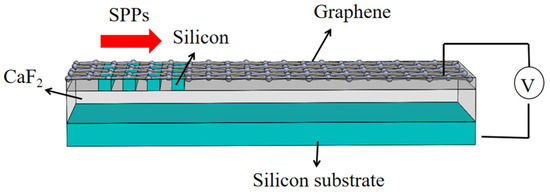
Figure 1.
The diagram of the designed substrate–dielectric–silicon–graphene structure.
2.2. Simulation Model
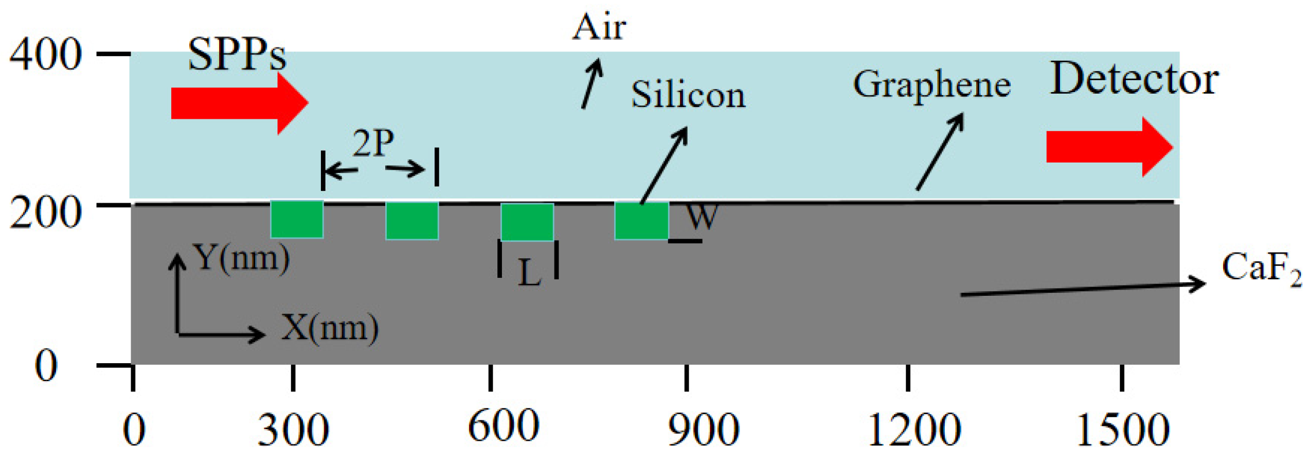
The simulation model we designed is shown in Figure 2. We used a two-dimensional model for simulation as the structure is symmetrical, which simplifies the computational workload. The SPPs are excited using port mode. The carrier density of the graphene is periodically doped due to the contact between the silicon and graphene, resulting in a periodic spatial distribution of the carrier density in the graphene. The overall carrier density in the graphene is modulated when a voltage is applied, resulting in different Fermi levels of the graphene. The influence of different lengths, widths, and periods of silicon grating at different Fermi levels and wavelengths was analyzed. The electric field distribution and optical transmission were utilized to observe the modulation performance. The P, L, and W represent the period, length, and width of the silicon grating, respectively.
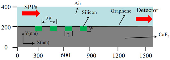
Figure 2.
Simulation model diagram.
3. Analysis of Simulation Results
3.1. Influence of Different Lengths
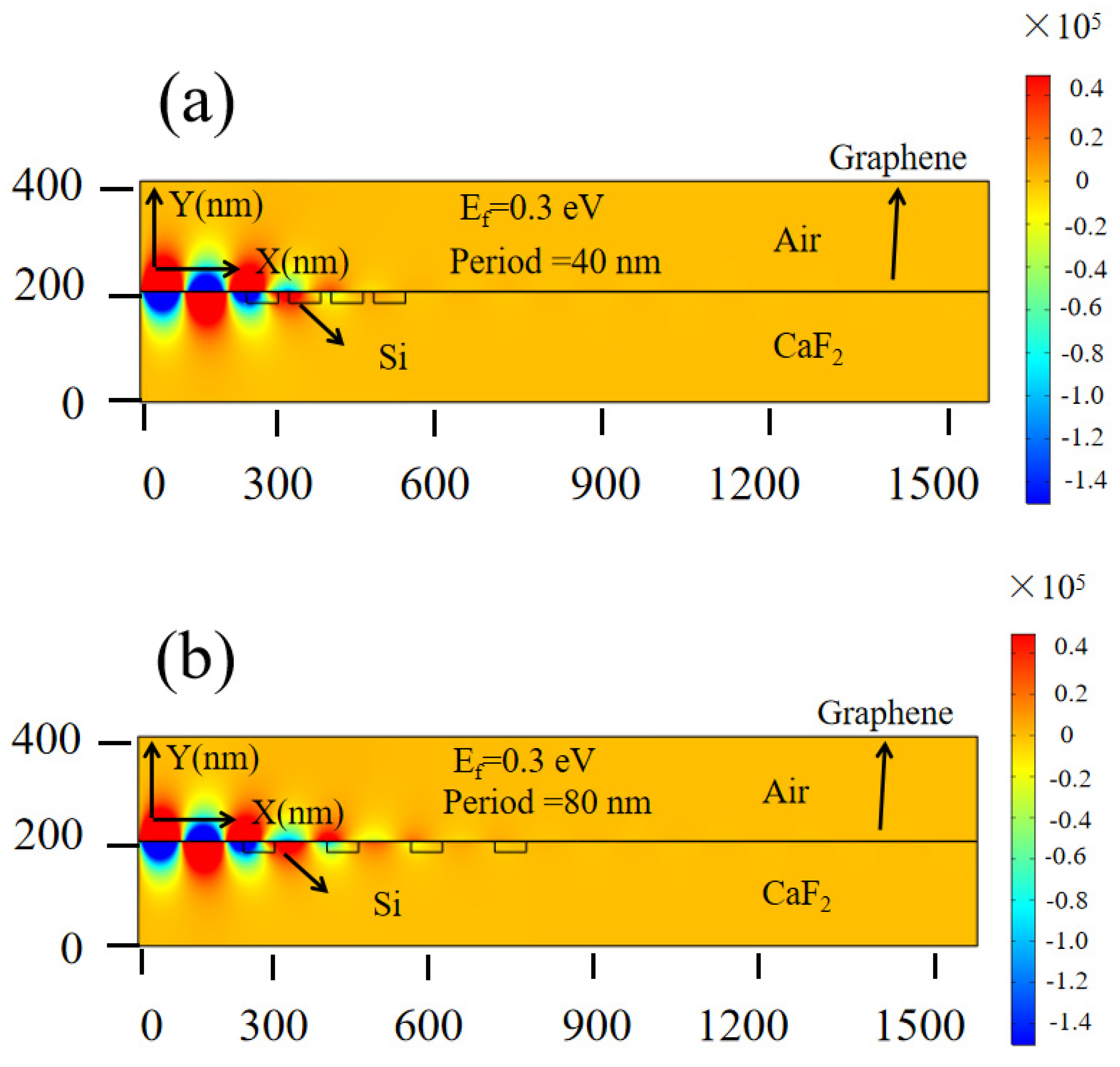
The graphene is chemically doped when the silicon grating interacts with it, resulting in the carrier density presenting a periodic distribution, which effectively influences the propagating SPPs. The difference in grating length affects the doping area directly; thus, the y component of the electric field presents various distributions. Figure 3a shows the y component of the electric field with a grating length of 10 nm and a Fermi level of 0.3 eV. Figure 3b shows the y component of the electric field with a grating length of 60 nm and a Fermi level of 0.3 eV (the width, grating period, and wavelength of the SPPs are fixed at 30 nm, 60 nm, and 8 μm, respectively). It can be clearly observed that different grating lengths have a significant impact on the propagating SPPs by comparing Figure 3a,b. At the same time, the overall carrier density can be modulated by the applied voltage. Figure 3c shows the y component of the electric field with a grating length of 60 nm while the Fermi level of the graphene is set to 0.9 eV. By comparing Figure 3b,c, it can be seen that, with the same length, the propagating SPPs can also be controlled dynamically via the applied voltage. This provides an additional dimension for modulating the SPPs and greatly improving performance.
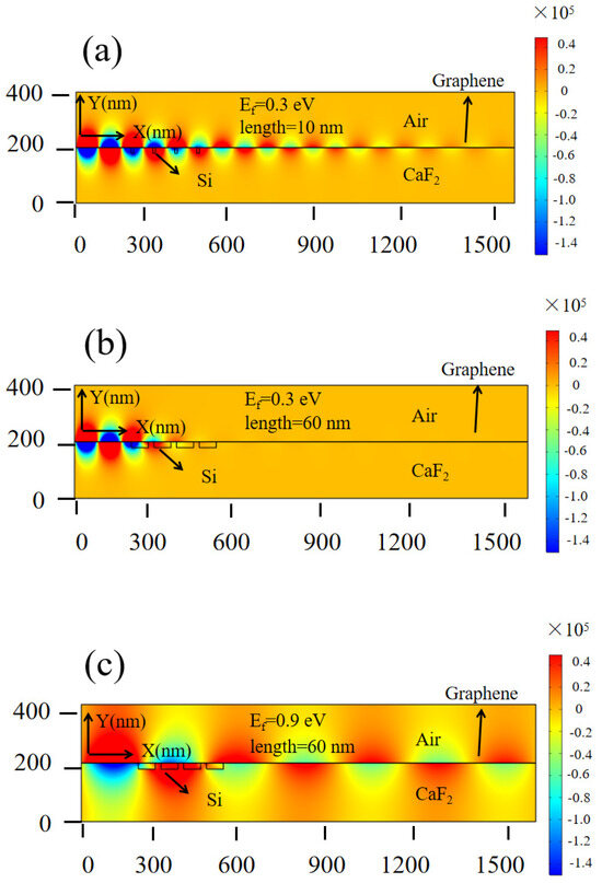
Figure 3.
The y component of the electric field at different parameters: (a) length = 10 nm. Ef = 0.3 eV; (b) length = 60 nm, Ef = 0.3 eV; (c) length = 60 nm, Ef = 0.9 eV.
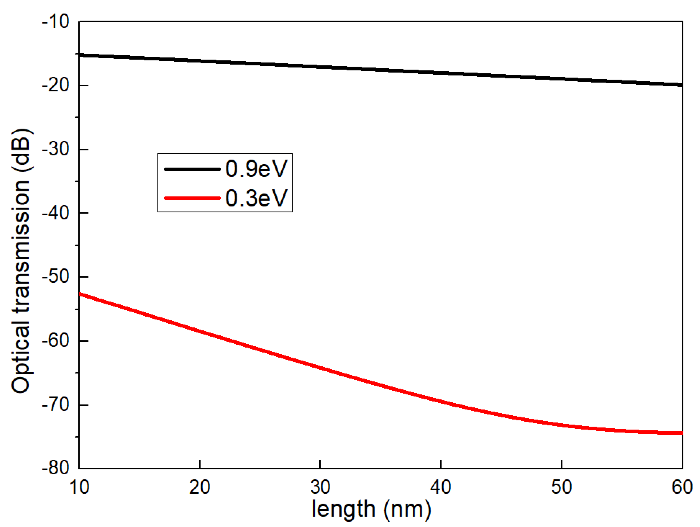
The modulation depth is significantly enhanced by integrating dynamic control of the overall carrier density through the application of varying voltages, and periodic control of the carrier density is achieved by designing silicon gratings of different lengths. The relationship between the optical transmission and various grating lengths at 0.3 eV and 0.9 eV is shown in Figure 4, with the optical transmission reaching its maximum value of 54.67 dB when the silicon grating length is 54 nm.
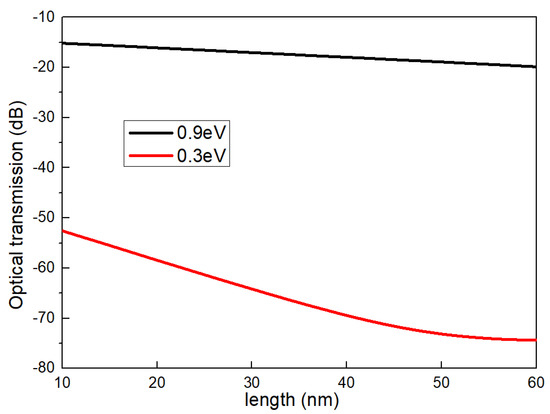
Figure 4.
The relationship between optical transmission and grating length.
3.2. Influence of Different Widths
The equivalent refractive index of silicon grating and graphene changes when the width of grating is different, resulting in a different scattering effect on the propagating SPPs. Figure 5a shows the y component of the electric field with a grating width of 10 nm and a Fermi level of 0.3 eV. Figure 5b shows the y component of the electric field with a grating width of 60 nm and a Fermi level of 0.3 eV (the length, grating period, and wavelength of the SPPs are fixed at 30 nm, 60 nm, and 8 μm, respectively). It can be clearly observed that different grating widths have a significant impact on the propagating SPPs by comparing Figure 5a,b. At the same time, the overall carrier density can be modulated by the applied voltage. Figure 5c shows the y component of the electric field with a grating width of 60 nm when the Fermi level of the graphene is set to 0.9 eV. It can be demonstrated that under the same width, the propagating SPPs can be further dynamically controlled via applying voltage by comparing Figure 5b,c, providing an additional dimension for modulating the SPPs and improving performance.
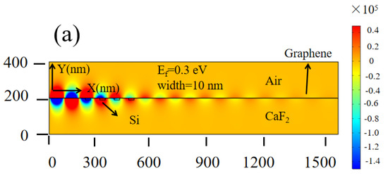
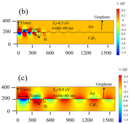
Figure 5.
The y component of the electric field at different parameters: (a) width = 10 nm, Ef = 0.3 eV; (b) width = 60 nm, Ef = 0.3 eV; (c) width = 60 nm, Ef = 0.9 eV.
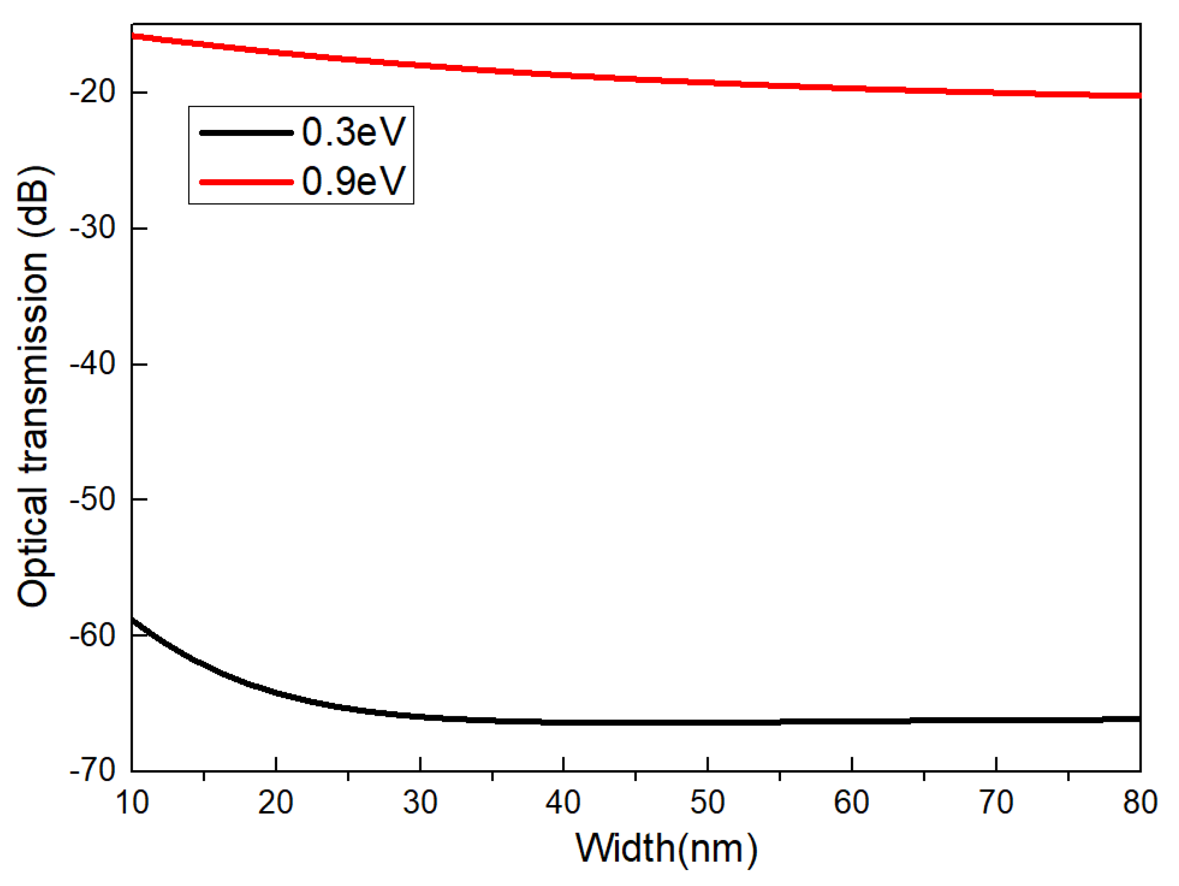
The grating width can affect the equivalent refractive index of the silicon grating and the graphene, resulting in a different scattering effect. The relationship between the optical transmission and different grating widths at 0.3 eV and 0.9 eV is depicted in Figure 6, with the optical transmission reaching its maximum value of 47.9 dB when the silicon grating width is 28 nm.
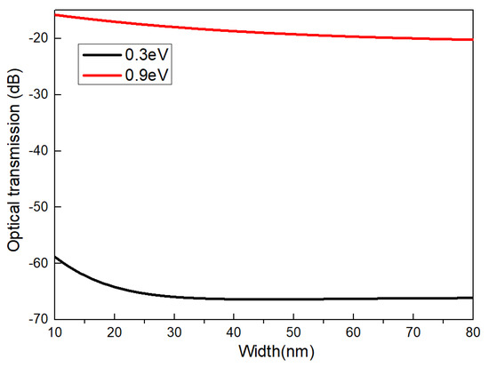
Figure 6.
The relationship between optical transmission and grating width.
3.3. Influence of Different Periods
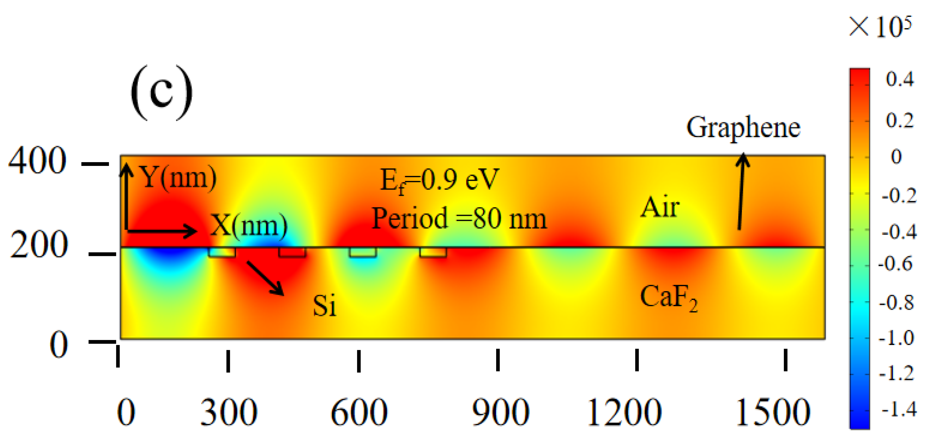
Different grating periods have various scattering effects on the propagating SPPs. Therefore, we investigated the change of the y component of the electric field at different periods. Figure 7a shows the y component of the electric field with a grating period of 40 nm and a Fermi level of 0.3 eV. Figure 7b shows the y component of the electric field with a grating period of 80 nm and a Fermi level of 0.3 eV (the length, width of the grating, and wavelength of the SPPs are fixed at 60 nm, 30 nm, and 8 μm, respectively). It can be clearly observed that different grating periods have a significant impact on the propagating SPPs by comparing Figure 7a,b, owing to the various distribution periods of carrier density. At the same time, the overall carrier density can be modulated by the applied voltage. Figure 7c shows the y component of the electric field with a grating period of 80 nm when the Fermi level of the graphene is set to 0.9 eV. By comparing Figure 7b,c, it can be observed that under the same period, the propagating SPPs can be further dynamically controlled via applying voltage.
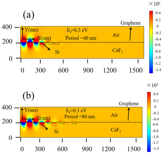

Figure 7.
The y component of the electric field at different parameters: (a) period = 40 nm, Ef = 0.3 eV; (b) period = 80 nm, Ef = 0.3 eV; (c) period = 80 nm, Ef = 0.9 eV.
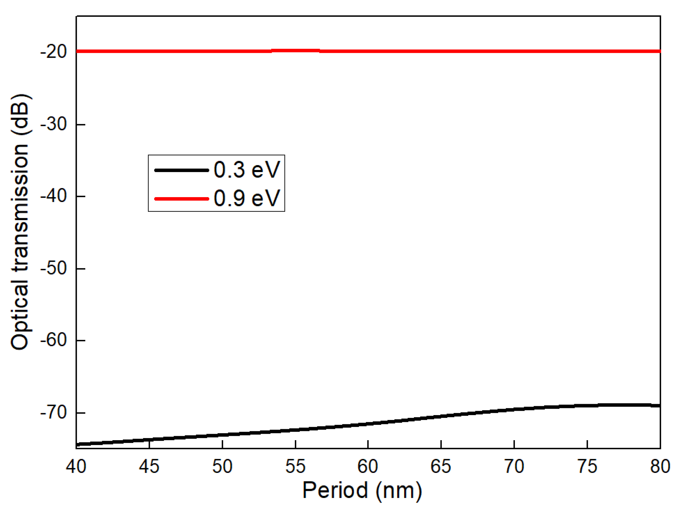
The grating period directly affects the distribution period of carrier density in graphene, resulting in a different scattering effect. The relationship between the optical transmission and different grating periods at 0.3 eV and 0.9 eV is shown in Figure 8, with the optical transmission reaching its maximum value of 54.5 dB when the grating period is 40 nm.
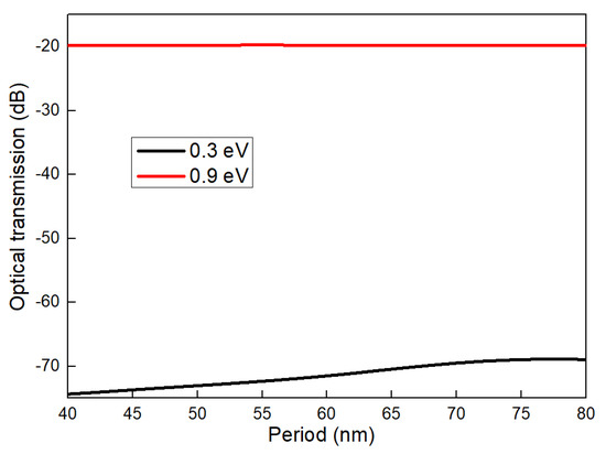
Figure 8.
The relationship between the optical transmission and grating period.
3.4. Influence of Different Wavelengths
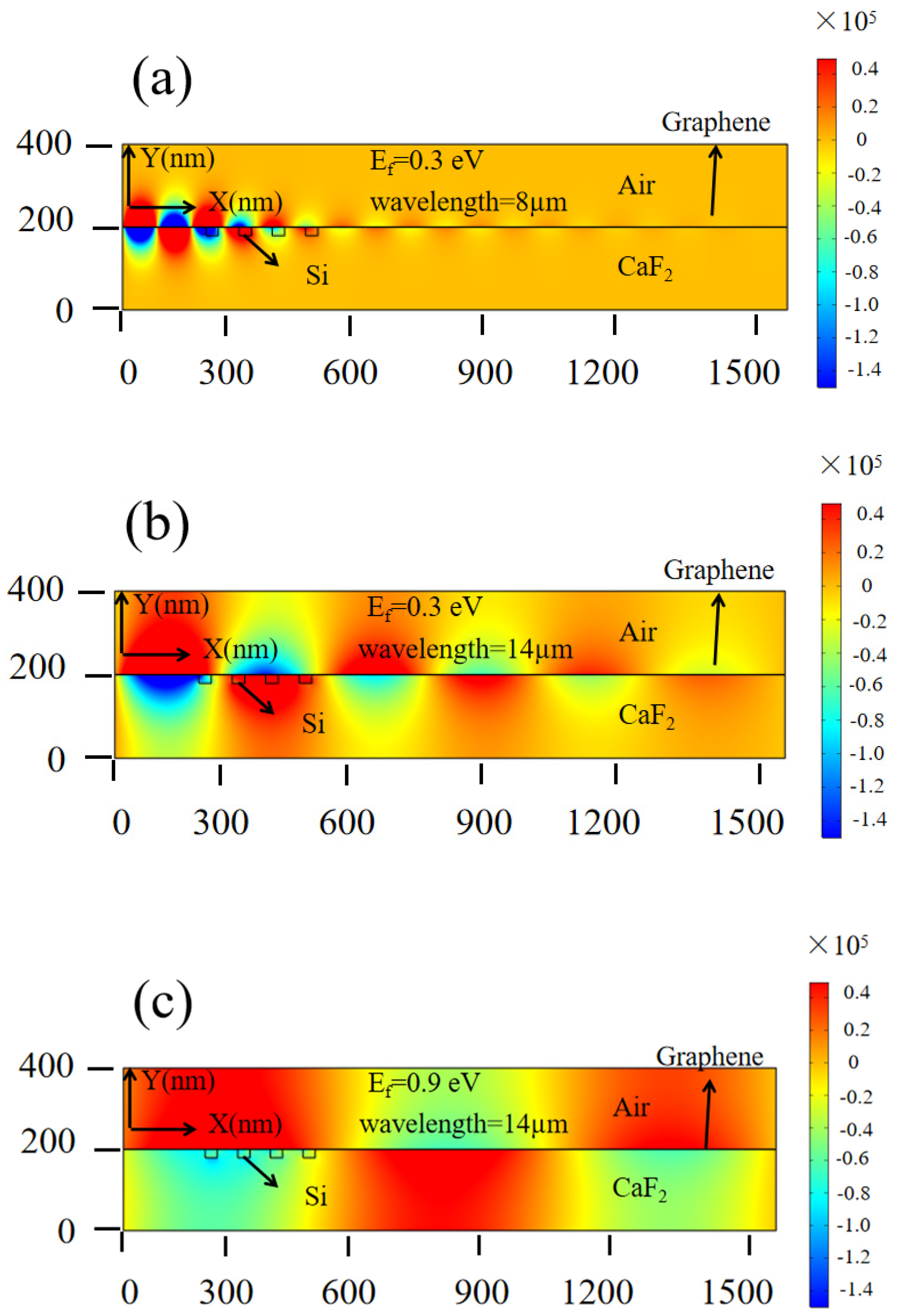
Both the periodic and overall distribution of carrier density have different influences on the propagating SPPs at various wavelengths. Figure 9a shows the y component of the electric field with a wavelength of 8 μm and a Fermi level of 0.3 eV. Figure 9b shows the y component of the electric field with a wavelength of 14 μm and a Fermi level of 0.3 eV (the length, width, and grating period are fixed at 30 nm, 30 nm, and 60 nm, respectively). By comparing Figure 9a,b, it can be clearly observed that the periodic distribution of carrier density has various impacts on the different wavelengths of the propagating SPPs. At the same time, the overall carrier density can be modulated by the applied voltage. Figure 9c shows the y component of the electric field with a wavelength of 14 μm when the Fermi level of the graphene is set to 0.9 eV. By comparing Figure 9b,c, it can be proved that under the same wavelength, the propagating SPPs can be further dynamically controlled via applying voltage.
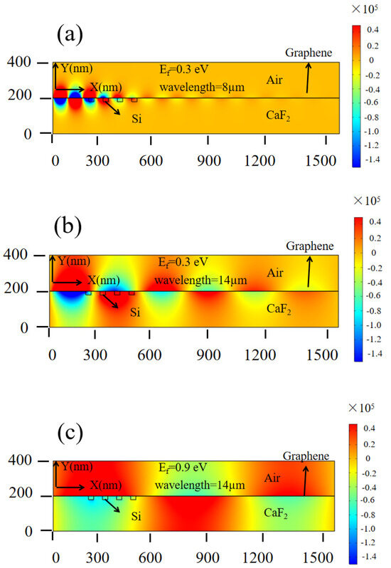
Figure 9.
The y component of the electric field at different parameters: (a) wavelength = 8 um, Ef = 0.3 eV; (b) wavelength = 14 um, Ef = 0.3 eV; (c) wavelength = 14 um, Ef = 0.9 eV.
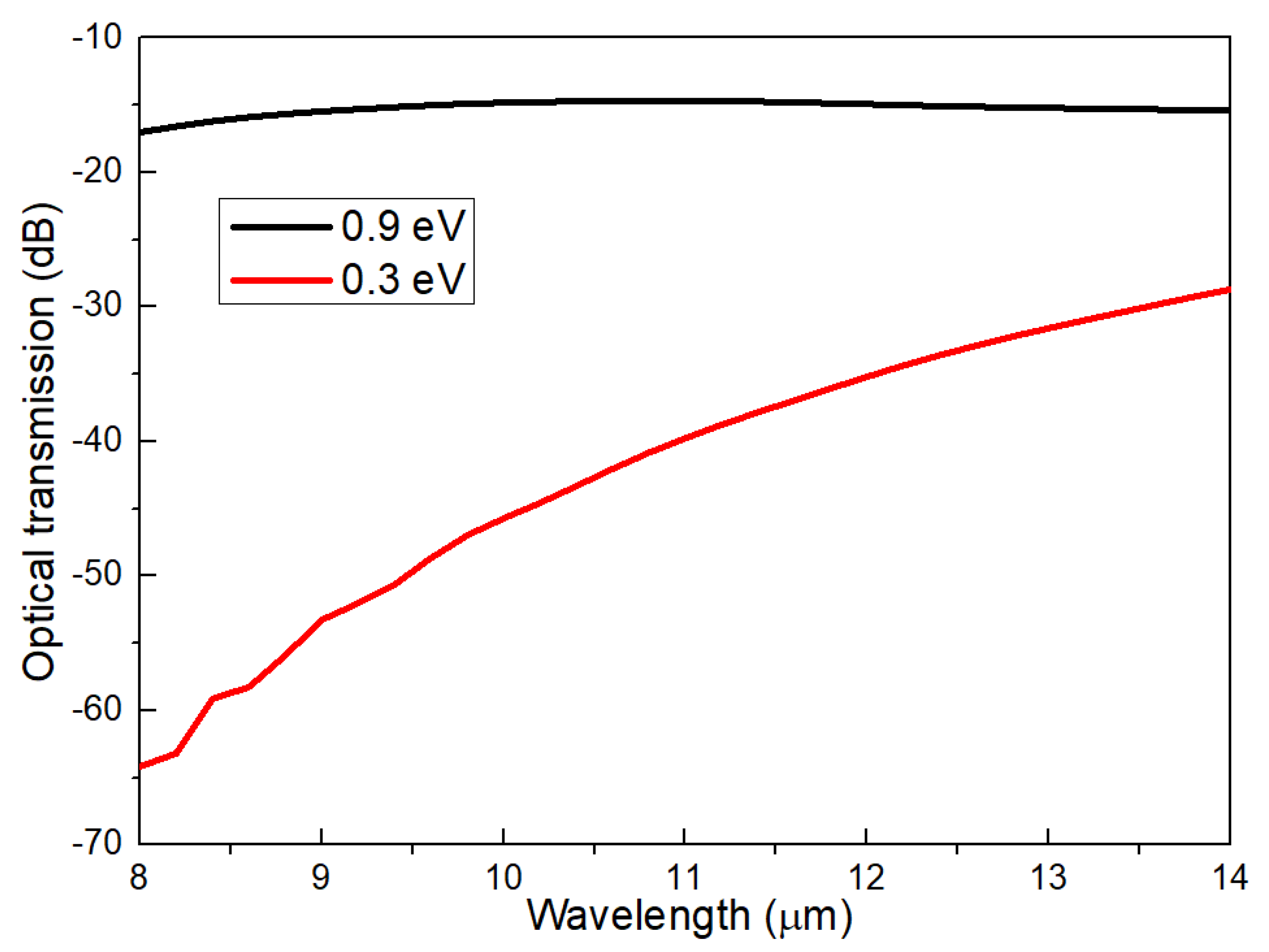
The distribution of carrier density has various scattering effects at different wavelengths. The relationship between the optical transmission and the wavelength of the SPPs at 0.3 eV and 0.9 eV, respectively, is shown in Figure 10, with the optical transmission reaching its maximum value of 47.2 dB at a wavelength of 8 μm.
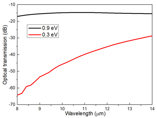
Figure 10.
The relationship between optical transmission and the wavelength of SPPs.
4. Conclusions
In summary, this article proposes a hybrid substrate–dielectric–silicon–graphene structure. On the one hand, the carrier density presents a periodic distribution due to the chemical doping of silicon grating. Herein, the length, width, and period of silicon grating can modulate the propagating SPPs in graphene. On the other hand, the overall carrier density distribution of graphene can be altered by applying a voltage between the substrate and graphene. The numerical results show that a significant improvement has been made in the modulation depth by using this dual-control mechanism. This structure has great potential for applications in optoelectronic sensing, optoelectronic detection, and optical modulation.
5. Methods
The simulation was performed using the commercial finite element method (FEM) and the trial version of the software “COMSOL Multiphysics 5.5”. In the simulation, scattering boundary conditions and a user-defined port were used. The radio frequency module was used to investigate the relationship between different parameters and the optical transmission and electric field distribution. The surface conductivity model and transitional boundary condition were used in the model of the graphene. In addition, the permittivity of CaF2 was set as 6.76. The mesh size was 1/5 of one wavelength.
Author Contributions
C.L. and S.Y. designed the study, Z.C. finished the numerical simulation, and M.L. and X.H. interpreted the results and wrote the manuscript. All authors have read and agreed to the published version of the manuscript.
Funding
This work was supported in part by the National Natural Science Foundation of China (NSFC) (12274075).
Data Availability Statement
The data relative to the experiments discussed in this work are available upon reasonable request from the corresponding author Sisi Yang.
Conflicts of Interest
The authors declare no conflicts of interest.
References
- Haffner, C.; Heni, W.; Fedoryshyn, Y.; Niegemann, J.; Melikyan, A.; Elder, D.L.; Baeuerle, B.; Salamin, Y.; Josten, A.; Koch, U.; et al. All-plasmonic Mach–Zehnder modulator enabling optical high-speed communication at the microscale. Nat. Photonics 2015, 9, 525–528. [Google Scholar] [CrossRef]
- Liu, M.; Yin, X.; Zhang, X. Double-Layer Graphene Optical Modulator. Nano Lett. 2012, 12, 1482–1485. [Google Scholar] [CrossRef] [PubMed]
- Ai, Z.; Liu, H.; Cheng, S.; Zhang, H.; Yi, Z.; Zeng, Q.; Wu, P.; Zhang, J.; Tang, C.; Hao, Z. Four peak and high angle tilted insensitive surface plasmon resonance graphene absorber based on circular etching square window. J. Phys. D Appl. Phys. 2025, 58, 185305. [Google Scholar] [CrossRef]
- Gan, X.; Shiue, R.J.; Gao, Y.; Mak, K.F.; Yao, X.; Li, L.; Szep, A.; Walker, D., Jr.; Hone, J.; Heinz, T.F.; et al. High-contrast electrooptic modulation of a photonic crystal nanocavity by electrical gating of graphene. Nano Lett. 2013, 13, 691–696. [Google Scholar] [CrossRef]
- Dionne, J.A.; Diest, K.; Sweatlock, L.A.; Atwater, H.A. PlasMOStor: A Metal-Oxide-Si Field Effect Plasmonic Modulator. Nano Lett. 2009, 9, 897–902. [Google Scholar] [CrossRef] [PubMed]
- Sun, X.; Zhou, L.; Zhu, H.; Wu, Q.; Li, X.; Chen, J. Design and Analysis of a Miniature Intensity Modulator Based on a Silicon-Polymer-Metal Hybrid Plasmonic Waveguide. IEEE Photonics J. 2014, 6, 1–10. [Google Scholar] [CrossRef]
- Shi, K.; Haque, R.R.; Zhao, B.; Zhao, R.; Lu, Z. Broadband electro-optical modulator based on transparent conducting oxide. Opt. Lett. 2014, 39, 4978–4981. [Google Scholar] [CrossRef] [PubMed]
- Li, Z.; Cheng, S.; Zhang, H.; Yang, W.; Yi, Z.; Yi, Y.; Wang, J.; Ahmad, S.; Raza, R. Ultrathin broadband terahertz metamaterial based on single-layer nested patterned graphene. Phys. Lett A 2025, 534, 130262. [Google Scholar] [CrossRef]
- Emani, N.K.; Chung, T.F.; Ni, X.; Kildishev, A.K.; Chen, Y.P.; Boltasseva, A. Electrically tunable damping of plasmonic resonances with graphene. Nano lett. 2012, 12, 5202–5206. [Google Scholar] [CrossRef]
- Brar, V.W.; Sherrott, M.C.; Jang, M.S.; Kim, S.; Kim, L.; Choi, M.; Sweatlock, L.A.; Atwater, H.A. Electronic modulation of infrared radiation in graphene plasmonic resonators. Nat. Commun. 2015, 6, 7032. [Google Scholar] [CrossRef]
- Gan, X.; Shiue, R.-J.; Gao, Y.; Meric, I.; Heinz, T.F.; Shepard, K.; Hone, J.; Assefa, S.; Englund, D. Chip-integrated ultrafast graphene photodetector with high responsivity. Nat. Photonics 2013, 7, 883–887. [Google Scholar] [CrossRef]
- Feigenbaum, E.; Diest, K.; Atwater, H.A. Unity-Order Index Change in Transparent Conducting Oxides at Visible Frequencies. Nano Lett. 2010, 10, 2111–2116. [Google Scholar] [CrossRef]
- Kim, S.; Jang, M.S.; Brar, V.W.; Tolstova, Y.; Mauser, K.W.; Atwater, H.A. Electronically tunable extraordinary optical transmission in graphene plasmonic ribbons coupled to subwavelength metallic slit arrays. Nat. Commun. 2016, 7, 12323. [Google Scholar] [CrossRef] [PubMed]
- Jiang, B.-Y.; Ni, G.-X.; Addison, Z.; Shi, J.K.; Liu, X.; Zhao, S.Y.F.; Kim, P.; Mele, E.J.; Basov, D.N.; Fogler, M.M. Plasmon Reflections by Topological Electronic Boundaries in Bilayer Graphene. Nano Lett. 2017, 17, 7080–7085. [Google Scholar] [CrossRef]
- Chauhan, D.; Sbeah, Z.; Dwivedi, R.P.; Nunzi, J.-M.; Thakur, M.S. An investigation and analysis of plasmonic modulators: A review. J. Opt. Commun. 2024, 45, 483–511. [Google Scholar] [CrossRef]
- Lan, G.; Tang, L.; Dong, J.; Nong, J.; Luo, P.; Li, X.; Li, Z.; Zhang, Y.; Dai, Y.; Wang, W.; et al. Enhanced Asymmetric Light-Plasmon Coupling in Graphene Nanoribbons for High-Efficiency Transmissive Infrared Modulation. Laser Photonics Rev. 2024, 18, 2300469. [Google Scholar] [CrossRef]
- Zemtsov, D.S.; Pshenichnyuk, I.A.; Kosolobov, S.S.; Zemtsova, A.K.; Zhigunov, D.M.; Smirnov, A.S.; Garbuzov, K.N.; Drachev, V.P. Plasmon-Assisted Si-ITO Integrated Electro-Optical Rib-Shape Modulator. J. Light. Technol. 2023, 41, 6310–6314. [Google Scholar] [CrossRef]
- Dhingra, N.; Mehrvar, H.; Berini, P. High-speed polarization-independent plasmonic modulator on a silicon waveguide. Opt. Express 2023, 31, 22481–22496. [Google Scholar] [CrossRef]
- Bareza, N., Jr.; Gopalan, K.K.; Alani, R.; Paulillo, B.; Pruneri, V. Mid-infrared Gas Sensing Using Graphene Plasmons Tuned by Reversible Chemical Doping. ACS Photonics 2020, 7, 879–884. [Google Scholar] [CrossRef]
- Abeysinghe, D.C.; Nader, N.; Myers, J.; Hendrickson, J.R.; Cleary, J.W.; Walker, D.E., Jr.; Chen, K.-H.; Liu, Y.; Mou, S. Edge Doping Effect to the Surface Plasmon Resonances in Graphene Nanoribbons. J. Phys. Chem. 2019, 123, 19820–19827. [Google Scholar] [CrossRef]
- Wang, Y.; Lu, M. Graphene surface plasmon bandgap based on two dimensional Si gratings. AIP Adv. 2017, 7, 1–3. [Google Scholar] [CrossRef]
- Tyagaraj, H.B.; Mahamiya, V.; Marje, S.J.; Safarkhani, M.; K, G.S.; Al-Hajri, E.; Chodankar, N.R.; Huh, Y.S.; Han, Y.-K. Waste-to-energy material: Winery-waste derived heteroatoms containing graphene-like porous carbon for high-voltage supercapacitor. Mater. Today Sustain. 2024, 27, 100901. [Google Scholar] [CrossRef]
- Kovalev, S.; Hafez, H.A.; Tielrooij, K.-J.; Deinert, J.-C.; Ilyakov, I.; Awari, N.; Alcaraz, D.; Soundarapandian, K.; Saleta, D.; Germanskiy, S.; et al. Electrical tunability of terahertz nonlinearity in graphene. Sci. Adv. 2021, 7, eabf9809. [Google Scholar] [CrossRef]
- Hu, X.; Lu, C.; Zhao, X.; Gu, Y.; Lu, M.; Sun, D. A multi-parameter tunable plasmon modulator. Sci. Rep. 2023, 13, 11483. [Google Scholar] [CrossRef] [PubMed]
- Hu, X.; Zhao, X.; Gu, Y.; Jin, S.; Shafqat, H.; Cui, Y.; Lu, C. A plasmon modulator by dynamically controlling the spatial distribution of carrier density in graphene. Opt. Commun. 2022, 513, 128093. [Google Scholar] [CrossRef]
- Zhu, L.; Fan, Y.; Wu, S.; Yu, L.; Zhang, K.; Zhang, Y. Electrical control of terahertz polarization by graphene microstructure. Opt. Commun. 2015, 346, 120–123. [Google Scholar] [CrossRef]
- Bao, Q.; Loh, K.P. Graphene photonics, plasmonics, and broadband optoelectronic devices. ACS Nano 2012, 6, 3677–3694. [Google Scholar] [CrossRef]
- Karimkhani, H.; Karim, M.A. Wide-band high performance optical modulator based on a stack of graphene and h-BN layers with plasmonic edge mode. Opt Quant Electron. 2025, 57, 1–23. [Google Scholar] [CrossRef]
- Forouzmand, A.; Mosallaei, H. Electro-optical Amplitude and Phase Modulators Based on Tunable Guided-Mode Resonance Effect. ACS Photonics 2019, 6, 2860–2869. [Google Scholar] [CrossRef]


Disclaimer/Publisher’s Note: The statements, opinions and data contained in all publications are solely those of the individual author(s) and contributor(s) and not of MDPI and/or the editor(s). MDPI and/or the editor(s) disclaim responsibility for any injury to people or property resulting from any ideas, methods, instructions or products referred to in the content. |
© 2025 by the authors. Licensee MDPI, Basel, Switzerland. This article is an open access article distributed under the terms and conditions of the Creative Commons Attribution (CC BY) license (https://creativecommons.org/licenses/by/4.0/).