Article

Integrated Bragg Grating Spectra

by
José Ángel Praena
1,* and
Alejandro Carballar
2
1
Ingeniería de Sistemas y Automática, Escuela Politécnica Superior, Universidad Pablo de Olavide, Ctra. Utrera km 1, 41013 Sevilla, Spain
2
Departamento de Ingeniería Electrónica, E.T.S. de Ingeniería, Universidad de Sevilla, c/Camino de los Descubrimientos, s/n, 41092 Sevilla, Spain
*
Author to whom correspondence should be addressed.
Photonics 2025, 12(4), 351; https://doi.org/10.3390/photonics12040351
Submission received: 25 February 2025 / Revised: 28 March 2025 / Accepted: 3 April 2025 / Published: 8 April 2025

Abstract

:
In this paper, we present a general methodology suitable for analyzing any IBG (Integrated Bragg Grating) as a linear time-invariant (LTI) system using the effective refractive index (ERI) and transfer matrix method (TMM). This approach is based on the translation of the IBG’s physical structure into a matrix of effective refractive indexes, neff, which is wavelength-dependent and describes the behavior of light in the IBG while avoiding the use of approximations like Coupled Mode Theory does. This procedure allows to obtain very accurate reflection and transmission spectra, regardless of the perturbation complexity of the grating. Using this methodology, different apodization and chirp methods are revised and compared. Its generality is considered by analyzing two distinct technological platforms, silicon-on-insulator (SOI) and aluminum oxide (Al2O3).

1. Introduction

Integrated Bragg Gratings (IBGs) are optical waveguides or photonic structures that implement a perturbation in their geometry, thereby achieving a modulation of the effective refractive index, neff, along the device length. As a result, IBGs can reflect specific wavelengths, acting as wavelength-selective reflectors or filters [1,2]. This functionality has made IBGs a keystone in photonic integrated circuits (PICs), enabling applications such as wavelength division multiplexing (WDM) [3], where they facilitate large-scale optical interconnections with low loss and high efficiency; optical sensing, including advanced biosensing [4], biophotonic applications [5], and spectroscopic sensing in the mid-infrared range [6]; and on-chip signal processing, such as reconfigurable photonic signal processors [7,8], integrated microwave photonics [9], and RF–optical hybrid systems [10].
The high refractive index contrast of platforms like silicon-on-insulator (SOI) and the moderately high refractive index of aluminum oxide (Al2O3) enable compact and efficient IBGs, but they also demand a rigorous analysis methodology [11,12]. Even nanometer-scale variations in the grating geometry can significantly impact the spectral response, making it essential to account for these details during the design phase to ensure optimal performance. This precision is particularly critical for advanced applications, such as Hilbert transformers [13], optical differentiators [14], integrators [15], and chromatic dispersion compensators [16], where the grating’s transfer function must be precisely tailored.
To achieve these complex spectral responses, it is necessary to modulate the neff with the corresponding complexity, which in turn requires the geometry of the IBG to be modified accordingly. This modulation of the IBG geometry, aimed at achieving a desired neff profile to elicit a specific transfer function, can be accomplished through techniques such as apodization and chirping. Apodization, for instance, reduces sidelobes in the reflection spectrum by gradually varying the grating strength along the device length [17]. Different apodization profiles, such as Gaussian, raised cosine, or hyperbolic tangent, have been explored to optimize performance. Similarly, chirping enables broadband reflection or dispersion compensation [18,19]. However, not all apodization and chirping strategies perform equally well, and their effectiveness depends on the specific application and fabrication platform [20]. Therefore, a robust and accurate analysis tool is indispensable for predicting the spectral response of IBGs before fabrication.
Traditionally, the analysis of IBGs has relied on the Coupled Mode Theory (CMT) [21,22], which simplifies the problem by leaving out the physical structure of the grating. Instead, it introduces a coupling constant κ to represent the strength of the interaction between forward and backward propagating modes. While CMT is computationally efficient and well-suited for long-length gratings like Fiber Bragg Gratings (FBGs) [23,24], it falls short in modeling the fine geometric details and wavelength-dependent behavior of IBGs. For example, CMT cannot accurately capture the impact of nanometer-scale variations in the grating structure, which are critical in high-index-contrast platforms [25]. These variations, which may arise from the design itself or occur randomly due to manufacturing constraints, can be as small as 5 nm. Moreover, although some wavelength-dependent extensions of CMT exist [26], they remain approximations that lack the precision required for modern PIC applications.
To address these limitations, the proposed analysis methodology is based on the model of the transfer and propagation matrix of electromagnetic waves in multilayer media characterized by its effective refractive index [20,27,28,29]. The procedure described in this work begins by mapping the IBG structure into a matrix of effective refractive indices (ERIs), which are functions of the wavelength and position along the IBG, neff(λ,z). Subsequently, the transfer matrix method (TMM) is applied to each layer and interface of the grating along the axis of optical wave propagation (z-axis). Finally, the spectral response, namely the transfer function, is obtained, achieving a good accuracy regardless of the grating’s complexity. This capability is particularly valuable for designing IBGs with customized transfer functions, such as those required for optical signal processing [30] or sensing applications.
The pertinence and generality of the proposed methodology (ERI-TMM) have been validated on two leading photonic platforms, SOI and Al2O3, for the fabrication of photonic integrated circuit (PIC) devices, demonstrating its versatility and robustness. SOI, with its high refractive index contrast and compatibility with CMOS fabrication processes, is ideal for dense integration and high-performance applications [1,2,31]. On the other hand, Al2O3 offers low propagation losses, a broad transparency window, and also compatibility with CMOS fabrication processes, making it highly suitable for applications in integrated photonics, including low-loss waveguides [32,33] and rare-earth doping for active devices [34]. By accurately modeling the wavelength-dependent refractive index and geometric variations, our approach provides a powerful tool for designing and optimizing IBGs across a wide range of applications.

2. Design of Integrated Bragg Grating

Before describing ERI-TMM, it is necessary to define the design parameters that characterize an IBG and that are used to achieve the expected spectral response. Depending on the material used by the chosen technology, they can take different values or even shapes. Moreover, their properties can vary depending on the wavelength. Our research centers on two specific materials and, consequently, two technologies: SOI and Al2O3. The working wavelength selected is within the third optical communications window, with a simulation spectral interval ranging from 1500 nm to 1600 nm. Figure 1a represents the geometrical structure of two uniform IBGs in SOI for a set of given parameters, and Figure 1b plots their power spectral responses (transfer functions) in reflection. The process from IBG geometry to IBG characterization as a linear-time invariant (LTI) system is known as an analysis procedure and is the subject of this work. It is important to note that the main characteristics of the spectrum, namely power response, bandwidth, Bragg wavelength, and extinction rate, can be affected in different ways by one or more of the IBG parameters. Therefore, a careful balance between them must be maintained during design.
The IBG geometry results in a variation of the waveguide width along the longitudinal axis (z-coordinate), which can be analytically represented by the following spatial expressions:
W z = W 0 z + Δ W ( z ) = W 0 z + Δ W m a x square 0 z 2 π Λ B ( z ) d z + φ z · A z
W z = W 0 z + Δ W ( z ) = W 0 z + Δ W m a x sin 0 z 2 π Λ B ( z ) d z + φ z · A z
These equations are valid for IBGs with symmetric perturbations at the upper and lower edges (Figure 1a). However, in the more general case, φ(z) can differ at both edges, resulting in φU(z) for the upper edge and φL(z) for the lower edge. Consequently, there will be different expressions for the upper WU(z) and lower WL(z) perturbations, and the general expression will be defined as W(z) = WU(z) + WL(z). As said, the parameters that form Equations (1) and (2) are used to map the apodization and chirp profiles onto the geometry of the IBG, that is, to modulate the effective refractive index neff(z) along the device length. Below, a detailed explanation of each parameter is given.

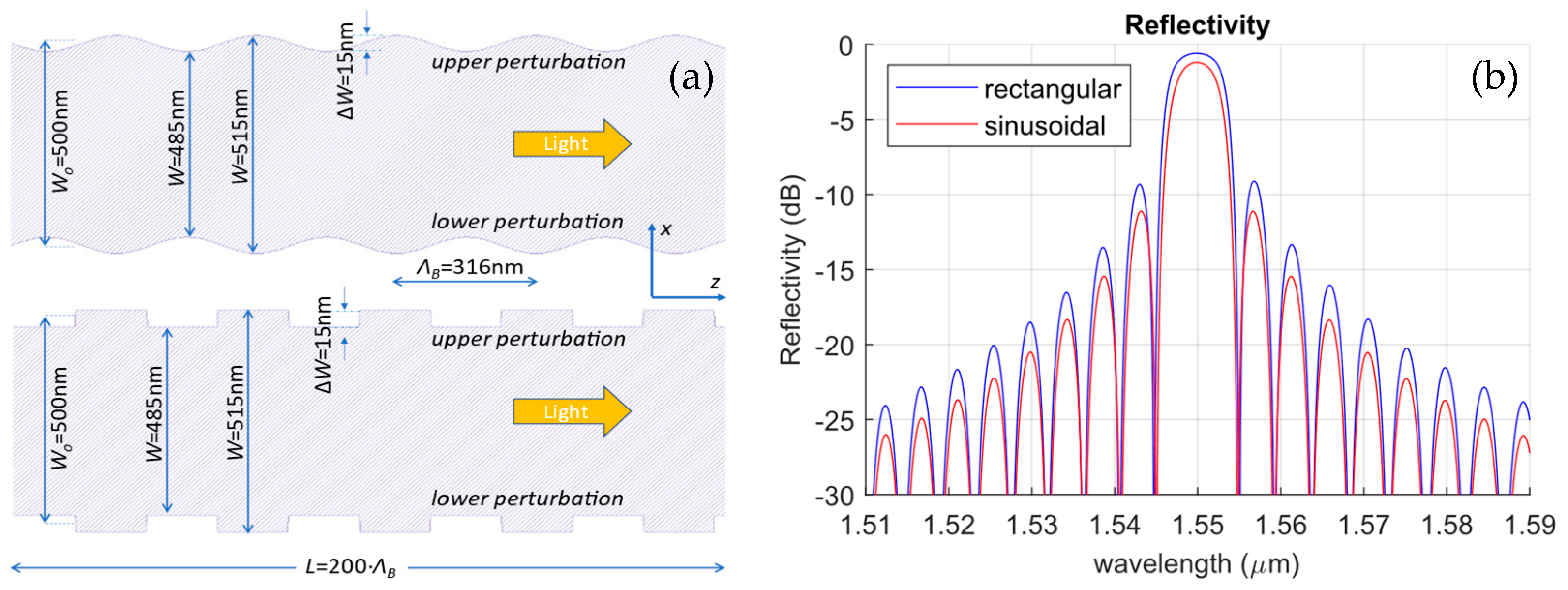
2.1. Corrugation Shape

It defines the shape of the periodic perturbation imposed on the IBG, typically described as rectangular in (1) or sinusoidal in (2). In the case of similar perturbations, rectangular corrugation achieves higher reflectivity, as shown in Figure 1b. However, as the perturbation increases, sinusoidal corrugation takes longer to reach the reflectivity saturation [20]. This effect can be explained by considering the proportionality between the effective refractive index and the reflectivity [1]. In rectangular corrugation, each Bragg half-period has the maximum neff throughout its entire area, while in sinusoidal perturbation, there is a continuous increase, and there is only one maximum in the middle of the period. Manufacturing constraints smooth the square angles of rectangular perturbations, a phenomenon that can be studied statistically and simulated using ERI-TMM [35].

2.2. Waveguide Width, W0(z)

It is the average width of the waveguide (length in the x-dimension), in other words, the waveguide width of the unperturbed IBG. When the value of W0(z) remains constant, it is referred to as W0. It controls the number of modes to be reflected. For example, in SOI technology, for W0 < 440 nm, there is no reflection (or transmission). For values of W0 between 440 nm and 550 nm, the behavior is single-mode, with only one TE and TM mode being reflected. And for W0 > 550 nm, the reflection is multimode [1]. This parameter determines the effective refractive index of the waveguide as a function of the wavelength. Typical values of W0 are 500 nm for SOI and 1100 nm for Al2O3.

2.3. IBG Corrugation Width, ΔW(z)

The increase or decrease in the x-dimension (see Figure 1a), over the waveguide width, is the perturbation itself. It is represented by the second term in Equations (1) and (2). Obviously, it is a key parameter because it allows us to map the perturbation profile onto the waveguide. The minimum value, ΔWmin, depends on the lithography resolution; in contrast, the maximum value, ΔWmax, must be experimentally determined for each technology. Corrugation width affects the bandwidth and amplitude of the reflectivity and is a function of z because it is defined by three parameters that indeed depend on z, as described as follows.

2.4. Bragg Period, ΛB(z)

It represents the length of the perturbation periodicity (period or pitch) applied in the z-dimension, which corresponds to the periodical variation imposed on the effective refractive index. ΛB(z) determines the Bragg wavelength (the peak of the main lobe of the spectrum in reflection, Figure 1b) through the following equation:
λ B m = 2 · n e f f λ B , W ( z ) · Λ B z m = 1 , 2 , 3
where m equals one, two, or three, representing the first, second, and third Bragg order, respectively. The expression of ΛB as a function of z implies the possibility of varying the Bragg period along the IBG, which will result in a chirp effect. Although Equation (3) is linear and quite simple, the dependance of λB on neff, which in turn depends on λB, introduces complexity into the calculations that ERI-TMM easily solves. For a detailed derivation of this equation, see [36]. Figure 2a provides a physical approximation of the relationship between the terms of expression (3). It illustrates that one period of the contra-directional optical wave (reflected wave) covers two Bragg periods of the IBG. The explanation lies in the phase-matching condition. According to Fresnel equations, the refraction coefficient at an interface for TE (transverse electric polarization) can be expressed as follows:
r T E = n 1 cos θ 1 n 2 cos θ 2 n 1 cos θ 1 + n 2 cos θ 2
For normal incidence, θ1 = θ2 = π/2, so
r T E = n 1 n 2 n 1 + n 2
When n1 < n2, the reflection coefficient becomes negative, which means a phase shift of π. When n2 < n1, there is no phase shift. In terms of layers, the accumulated phase is π/2, so for λB, the total phase accumulated in a round-trip is 2π, and there are constructive interferences in reflection (Figure 2b). For TM (transverse magnetic polarization), the reasoning is similar.
As already stated, the Bragg wavelength given by (3) for m = 1 is the first-order Bragg wavelength. Higher Bragg orders can be calculated as λB/m, where m is an integer number [37]. These new orders can also be explained graphically, also shown in Figure 2b, considering that the wavelengths to be reflected must always accumulate an integer multiple of 2π. The rest of the wavelengths, which do not undergo constructive interference in reflection, are canceled in reflection and hence fully transmitted.
This behavior helps demonstrate why the longer the grating, the narrower the bandwidth in reflection and the higher the power in reflection. As the length of the waveguide increases, the number of periods in which the reflected wavelengths are in phase increases, resulting in a corresponding reduction in the amount of energy transmitted (without energy loss, except for that which may be due to absorption from the medium). At the same time, the filter becomes more selective, as the accumulated phase of the wavelength to be reflected must align more closely with a phase increment that is an integer multiple of 2π. In other words, the filter has more periods to accumulate phases for those wavelengths that are in phase. So, one comes to the conclusion that when the number of Bragg periods increases (i.e., the IBG length increases), the number of interfering reflections increases, and the constrained interference criteria provide better selectivity in reflection and hence a narrower bandwidth.

2.5. Apodization Function, A(z)

It defines the envelope of the periodic perturbation ΔW(z), so it is used to apodize the grating. Different functions are used to smoothly increase or decrease the amplitude of ΔW(z), including the square cosine, the Gaussian and the hyperbolic tangent, among others. When there is no apodization, it is said to be a uniform IBG, meaning there is no modulation or variation in the amplitude of the perturbation, i.e., A(z) = 1.

2.6. Grating Phase, φ(z)

This parameter is certainly the most subtle. It defines the phase shift of the spatial periodic function and can be a function of z. As A(z), it can be used to apodize the IBG (i.e., to map the neff profile); although in this case it does not affect the amplitude of the geometric perturbation. The grating phase can be the same for the upper and lower edges of the grating or different (φU(z) and φL(z)), and some apodization methods exploit this phase variation to implement the apodization itself.

2.7. Grating Length, L

It represents the total length of the IBG, and usually, it is expressed in terms of Bragg periods. As just explained, it controls the bandwidth and also the power of reflectivity. Therefore, a trade-off must be made between L and ΔW(z) to meet the design requirements. For chirped IBG, L determines the group delay; the longer the IBG, the higher the phase shift and hence the group delay.

3. Methodology: Modeling and Simulation

The ERI-TMM represents a powerful and convenient mathematical formalism for determining the planewave reflection and transmission characteristics of an infinitely extended slab of a linear material in electromagnetics and optics [38,39,40]. The conventional TMM approach for analyzing FBG is based on CMT [21,22], in which the different grating layers are defined by their coupling coefficients, thus ignoring the physical structure [41]. Nevertheless, as stated before, the apodization of IBGs is achieved through geometrical variations in their structure, which can be as small as a few nanometers. Similarly, modifications in the grating phase must be considered, given their significant impact on the spectral response of IBGs.
This section describes the methodology proposed in the application of the transfer matrix method based on the effective refractive index for the analysis of IBG spectra, ERI-TMM. This procedure for modeling and simulation of an IBG is presented in a series of steps. Table 1 outlines the general features and parameters to be used, along with their common values.

3.1. Characterization of the Effective Refractive Index of an Optical Waveguide

The neff in an optical waveguide is a function of the wavelength and their geometrical features. To obtain it, we have used the software Lumerical® 2021 R2.3 [42], where the physical structure and constituent materials must be specified. The first step is to define and introduce the geometry of the transverse section of the waveguide. Then, a modal analysis, considering a plane wave propagation model, is carried out to achieve the real and imaginary part of the neff for the central wavelength (1550 nm). After that, a wavelength sweep is performed to obtain a vector of values neff(λ,Wi) for a given Wi. The values obtained are complex numbers of the form: neff(λ) = Re(neff) + j·Im(neff). The imaginary part is related to the attenuation of the medium, whereas the real part represents the effective refractive index, in other words, how the medium affects the phase of the optical field at each wavelength for an optical waveguide width Wi. A common way to express it is
k 0 n e f f λ = k 0 R e n e f f λ + k 0 I m n e f f λ = β λ j α ( λ ) / 2
This equation determines the relationship between the complex effective refractive index, the propagation constant in vacuum (k0), and the propagation (β) and attenuation (α) constants in the medium, where k0 = 2π/λ0, λ0 being the wavelength in vacuum.
The third step involves repeating the same procedure for different waveguide widths, specifically within the range from W0 − ΔWmax to W0 + ΔWmax. Repeating the procedure as described results in the matrix N, which contains the values of neff as a function of the wavelength and of the width, i.e., neff(λ,W), that characterizes the waveguide.

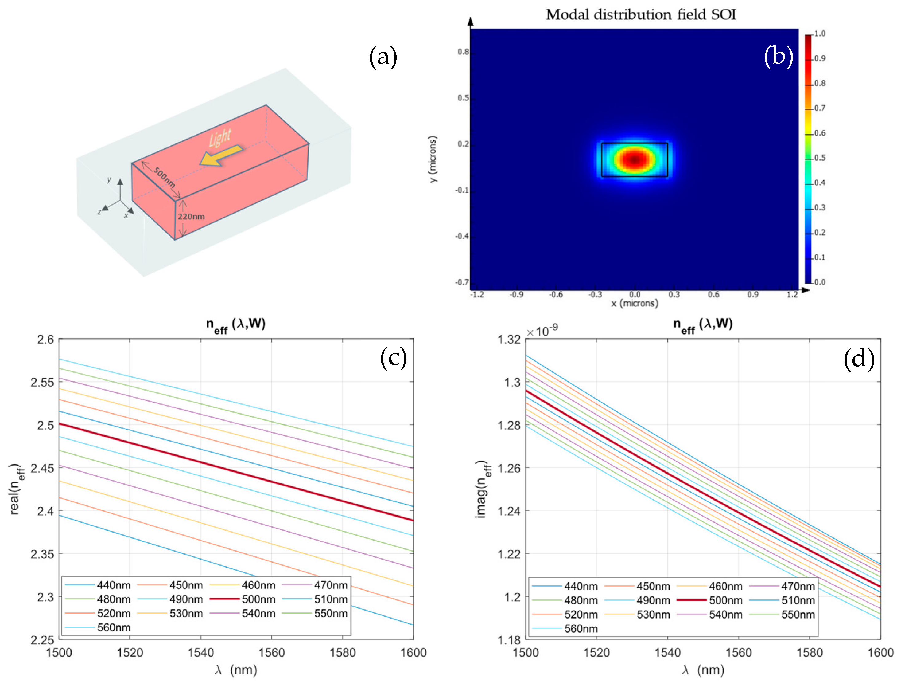
3.1.1. The SOI Optical Waveguide

The geometry for the SOI optical waveguide consists of a strip waveguide with a rectangular cross-section perpendicular to the direction of light propagation (see Figure 3a). The core is made of silicon with dimensions of 500 × 220 nm, while the cladding material is silica, SiO2. Thereby, the modal analysis is performed (as shown in Figure 3b) for an initial width of 500 nm and a wavelength of 1550 nm, achieving a complex effective refractive index. As anticipated, the transmission of light is single-mode, as verified by the energy carried in each mode. After sweeping the wavelengths, the plots in red in Figure 3c,d are obtained, representing neff(λ, 500 nm). Repeating the same process for different waveguide widths yields all the plots shown in Figure 3c,d, which represent the content of matrix N, that is, neff(λ,W).

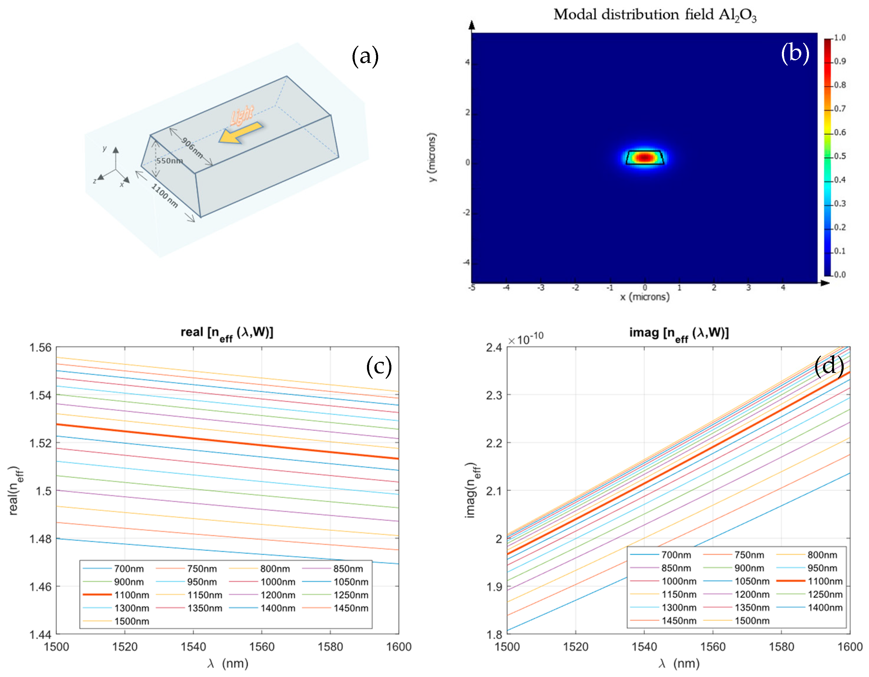
3.1.2. The Al2O3 Optical Waveguide

For Al2O3, the geometry consists of a strip waveguide with a trapezoid cross-section perpendicular to the direction of light propagation (see Figure 4a). Now, the core is made of Al2O3 (grey area in Figure 4a) with a major base of 1100 nm, a minor base of 906 nm, and a height of 550 nm, while the cladding material is made of SiO2. Again, modal analysis is performed (as shown in Figure 4b), in this case, on Al2O3 for a waveguide width of 1100 nm and wavelength of 1550 nm, achieving the complex effective refractive index. After sweeping the wavelengths, the plots in orange with thick lines in Figure 4c,d are obtained, representing neff(λ, 1100 nm). Repeating the same process for different waveguide widths yields all the plots shown in Figure 4c,d, which represent the content of matrix N, that is, neff(λ,W), for Al2O3.
Although it is beyond the scope of this article, it is interesting to observe the behavior of the imaginary part of the effective refractive index (the attenuation) given they are different materials. For SOI, attenuation increases with wavelength, whereas for Al2O3, attenuation decreases with wavelength.

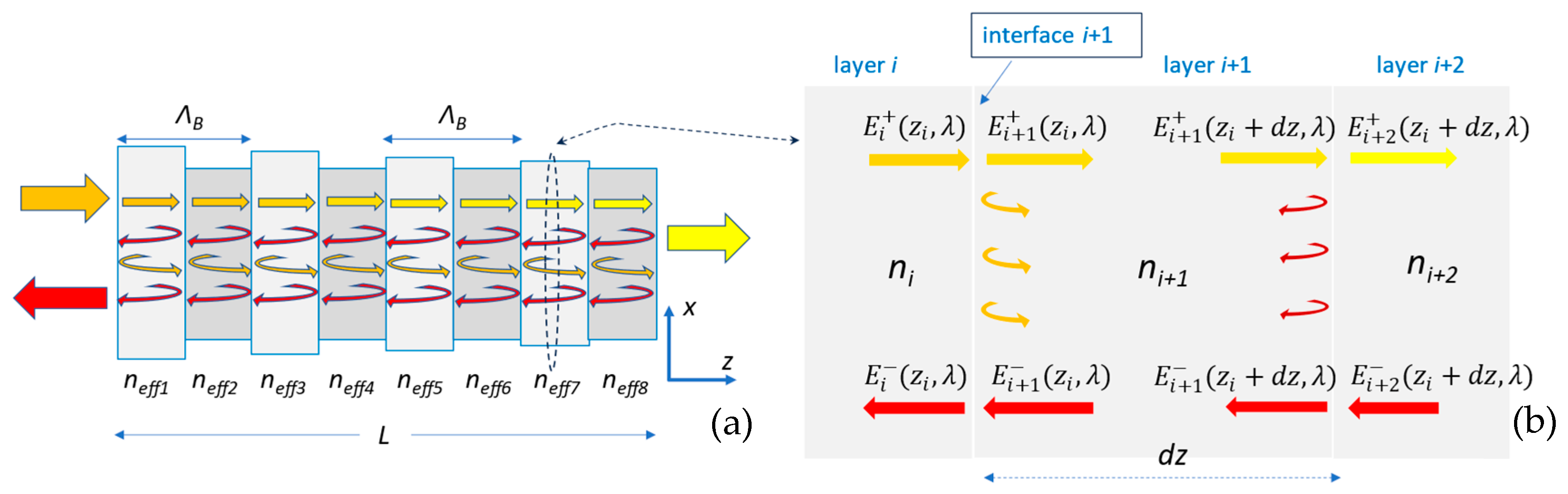
3.2. Sampling and Modeling of the IBG

Once the matrix N has been obtained for a certain technology, the modeling of the IBG under study can begin. To model the IBG, the effective refractive index must be calculated as a function of the position z, considering the variation of the neff with wavelength
n e f f λ , z = n e f f λ , W z
where W(z) is the general expression representing the geometry of an IBG, given by Equations (1) and (2). Having obtained the width of the grating as a function of z, the next step is to translate it into neff(λ,z) using the matrix N. To achieve this, the specific IBG structure must be sampled. The objective is to account for any minor variation in its geometry and even try to incorporate potential fabrication errors. Therefore, the strategy is to divide the IBG into many uniform sections (thin films) of constant length, dz, along the z-axis, considering that the more complex the geometry, the greater the number of sections that are required to model the IBG accurately. For example, for SOI, in the case of e-beam lithography, the resolution of the process is approximately 6 nm; hence, in order to capture any detail of the grating, it is necessary to consider about 48 layers for every Bragg period, which is equivalent to a dz ≈ 6 nm (this is the value used for the simulations along this paper). Furthermore, the method allows for working with even smaller dz values to ensure the inclusion of any feature and accurate representation of the grating, although this implies a longer processing time.
The result is arranged in a new matrix, N′, of size n × m that models the whole IBG. The rows are the array of effective refractive index values for different positions along the IBG, neff(zi); where dz = zi+1zi (0 < i < m) and the value of m is equal to the number of layers in which the IBG has been sampled. The columns contain the effective refractive index dependence on wavelength, neff(λj), with n being the number of wavelengths selected in the spectral range [1500 nm, 1600 nm]. Figure 5a shows a diagram of a general apodized IBG. The width of the IBG varies along its length, and so does the neff. In Figure 5b, a sample of the section with neff7 is zoomed in, illustrating the distribution of the fields.

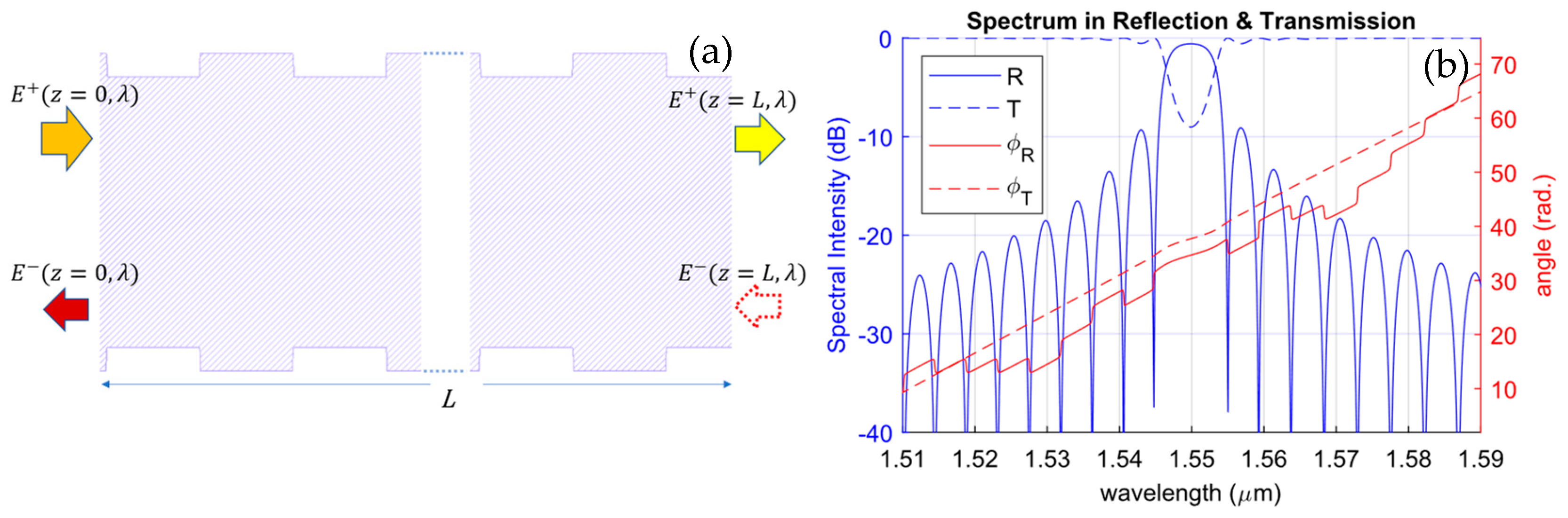
3.3. Calculating the Transfer Matrix of the IBG, MT

After having divided the IBG into n layers and interfaces between them, the following fields equations are going to be calculated at each one:
E i + ( z i , λ ) E i ( z i , λ ) = I i E i + 1 + ( z i , λ ) E i + 1 ( z i , λ )
E i + 1 + ( z i , λ ) E i + 1 ( z i , λ ) = C i + 1 E i + 1 + ( z i + d z , λ ) E i + 1 ( z i + d z , λ )
I i = 1 2 n i n i + n i + 1 n 1 n i + 1 n 1 n i + 1 n 1 + n i + 1
C i + 1 = e i λ n i + 1 d z 0 0 e i λ n i + 1 d z
In that way, every interface and layer is characterized by its matrix Ii and Ci, respectively. The effective refractive index on both sides of each interface i is given by the columns of N′, n(zi,λ), and n(zi+1,λ), while the co-directional (transmitted) and contra-directional (reflected) fields are represented by Ei+ and Ei, respectively, as illustrated in Figure 5b. The matrix that characterizes each pair layer plus interface is calculated as follows:
M i = I i · C i + 1 0 < i n
where the coefficients of Mi are complex functions that depend on the wavelength:
M i λ = t 11 i λ t 12 i λ t 21 i λ t 22 i λ
Finally, to obtain the matrix of the entire IBG that expresses the relation between the co-directional and contra-directional fields, the previous n matrices must be multiplied as follows:
M T λ = t 11 T λ t 12 T λ t 21 T λ t 22 T λ = M 1 λ · M 2 λ · · M n λ

3.4. Obtaining the Transfer Functions of the IBG

The matrix MT allows expressing the relation between the fields at the input and output of an IBG of length L in the following form:
E + ( z = 0 , λ ) E ( z = 0 , λ ) = t 11 T λ t 12 T λ t 21 T λ t 22 T λ E + ( z = L , λ ) E ( z = L , λ )
Let us consider a generic IBG characterized by its transfer matrix MT, which relates the complex field amplitudes at the input (z = 0) and output (z = L) of the grating. It is assumed that the structure is excited at one end E+(z = 0, λ); under these conditions, there can be no field amplitude at the other end E(z = L, λ) = 0 (see Figure 6a).
Consequently, with these boundary conditions, the reflection and transmission coefficients (reflection and transmission transfer functions) can be obtained from the characteristic transfer matrix of the structure by means of the following expressions:
H r λ = E z = 0 ( λ ) E z = 0 + ( λ ) E z = L = 0 = t 21 T ( λ ) t 11 T ( λ ) = H r λ e j ϕ r ( λ ) = R   ( λ ) · e j ϕ r ( λ )
H t λ = E z = L + ( λ ) E z = 0 + ( λ ) E z = L = 0 = 1 t 11 T ( λ ) = H t λ e j ϕ t ( λ ) = T   ( λ ) · e j ϕ t ( λ )
where Hr(λ) and Ht(λ) are complex functions, with module R(λ) and T(λ), that correspond to the reflectivity and transmissivity, with ϕr(λ) and ϕt(λ) being the associated phase functions. The group delay in reflection and transmission is calculated by taking the derivative of the phase functions with respect to the wavelength:
τ r λ = λ 2 2 π c d ϕ r λ d λ
τ t λ = λ 2 2 π c d ϕ t λ d λ
Figure 6b shows the graphical representation of the calculated spectral response in reflection and transmission of a uniform IBG using the described ERI-TMM.

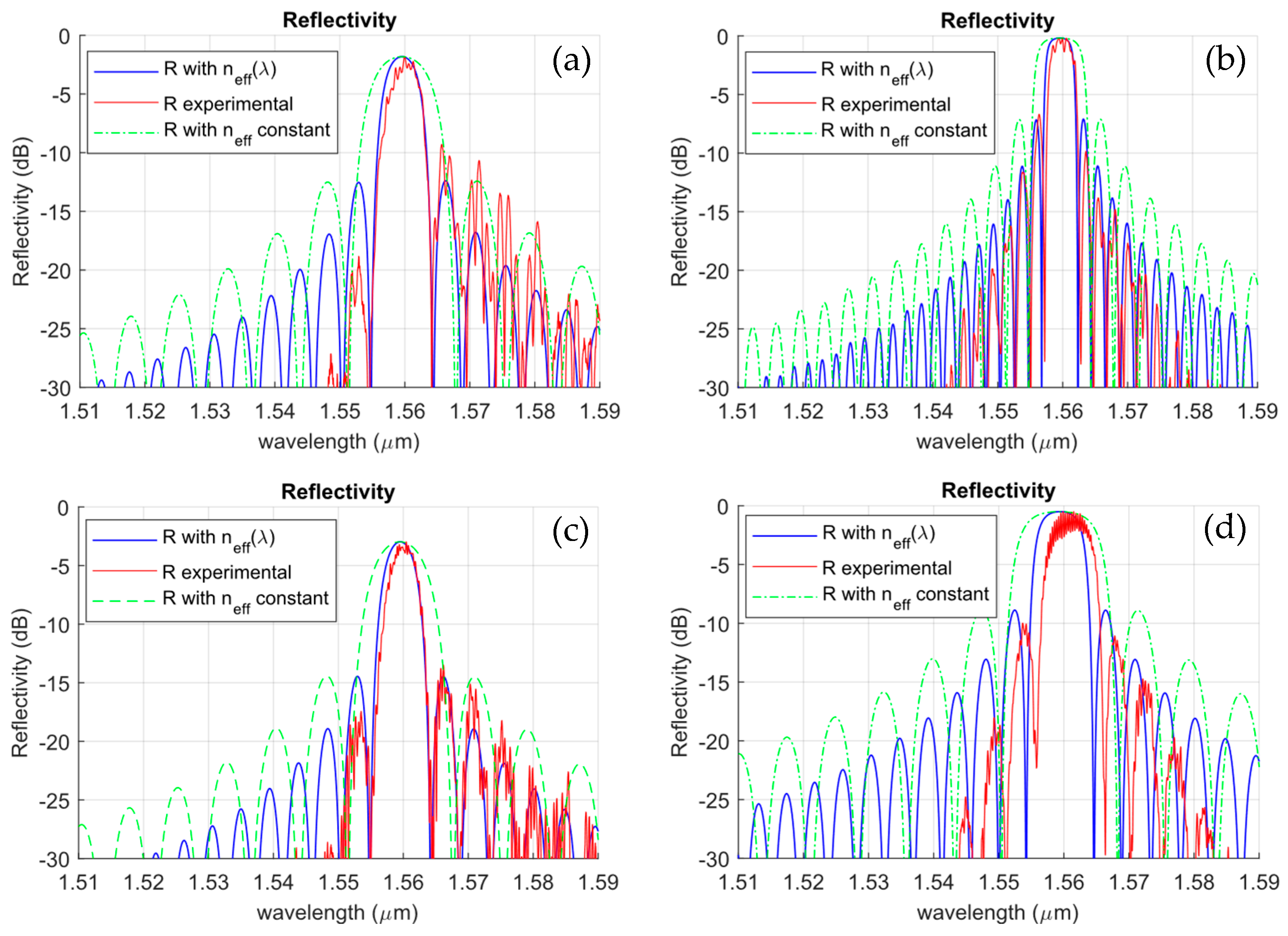
4. Experimental Results: Uniform IBGs

The agreement of the method with the experimental results has been validated using a set of measurements on IBGs fabricated by electron-beam lithography in SOI, following the coordination and process design kit provided by the SiEPIC program (www.siepic.ubc.ca (accessed on 18 December 2024) [43]. The wafer consisted of a series of uniform sinusoidal and rectangular IBGs, with corrugation widths ranging from 5 nm to 100 nm, ΛB = 317 nm, and lengths of 200ΛB and 400ΛB. The geometry was of a strip waveguide with a cross-section of 220 nm × 500 nm (see Section 3.1.1). Selected results are plotted in Figure 7, where three datasets are represented: the experimental measured reflectivity (red line), the simulated spectrum using ERI-TMM (blue line), and the simulated spectrum with neff kept constant with wavelength (dotted green line). Figure 7a shows the reflectivity of an IBG with rectangular perturbation, L = 200ΛB, and ΔW = 10 nm. Figure 7b plots the reflectivity for the same IBG but with double the length. Figure 7c presents the reflectivity for a sinusoidal IBG with L = 200ΛB and ΔW = 10, and Figure 7d depicts the same IBG but with ΔW = 20 nm. As can be observed, the simulated reflectivity using ERI-TMM agrees with the experimental data.
It is relevant to highlight that these results (and the simulations in accordance with them) demonstrate that if the neff wavelength dependence is not taken into account (as is commonly performed in FBG analysis), the results do not align with the experimental data. On the other hand, using ERI-TMM, the simulated spectrum agrees quite well with the experimental results, both in terms of Bragg wavelength and bandwidth.
Figure 7 allow us to observe the theoretical statement expressed above in relation to the increase in reflectivity and the reduction in its bandwidth as the IBG length increases, as well as how the proposed method fulfills this. It also shows, as the method predicts, a higher reflectivity for IBGs with rectangular perturbation compared to sinusoidal ones. Figure 7c,d demonstrate that an increase in the perturbation width results in greater reflectivity and bandwidth. In both cases, there is agreement with experimental results.
It is worth highlighting that, regarding the experimental reference setup, Figure 7 reveals discrepancies between theoretical and experimental data, particularly in the asymmetric sidebands relative to the central frequency. This behavior is certainly caused by the asymmetric response of the wavelength-dependent grating couplers used in the assembly, which transfer light from the waveguide to the input optical fiber, subsequently connected to the output and the optical spectrum analyzer (OSA) for measurements. While this visually apparent discrepancy is observable, its practical impact remains negligible for most IBG applications, as device performance primarily depends on main lobe characteristics. Moreover, the sidebands where these discrepancies appear exhibit attenuation exceeding 20 dB, effectively suppressing their influence.

5. Advanced Simulation Results I: Apodization Techniques for an IBG

After the ERI-TMM was validated with experimental data from uniform IBGs, the analysis proceeds to examine apodized IBGs. For this purpose, the most common apodizing techniques are outlined and simulated in SOI technology. This topic, apodization, is extensively covered in the literature [13,44,45,46,47,48]; therefore, the aim here is not to analyze these techniques but to demonstrate how ERI-TMM can accurately simulate the spectral responses of each, considering their nuances.
The term apodization is defined as the process of mapping a given neff profile onto the geometry of a waveguide, through the modulation of one or more of its characteristic parameters, with the objective of achieving a desired spectral response. The different apodization techniques appear as a result of the strategic approach followed for this modulation. Figure 8 illustrates four apodization methods: corrugation width modulation, lateral delay modulation, duty cycle modulation and phase delay modulation. It is common to confuse the term “apodization functions” (some examples are listed in Table 2) with apodization methods or techniques. As mentioned, the latter involves different ways of obtaining not only different apodization functions but also tailored spectral responses or transfer functions.

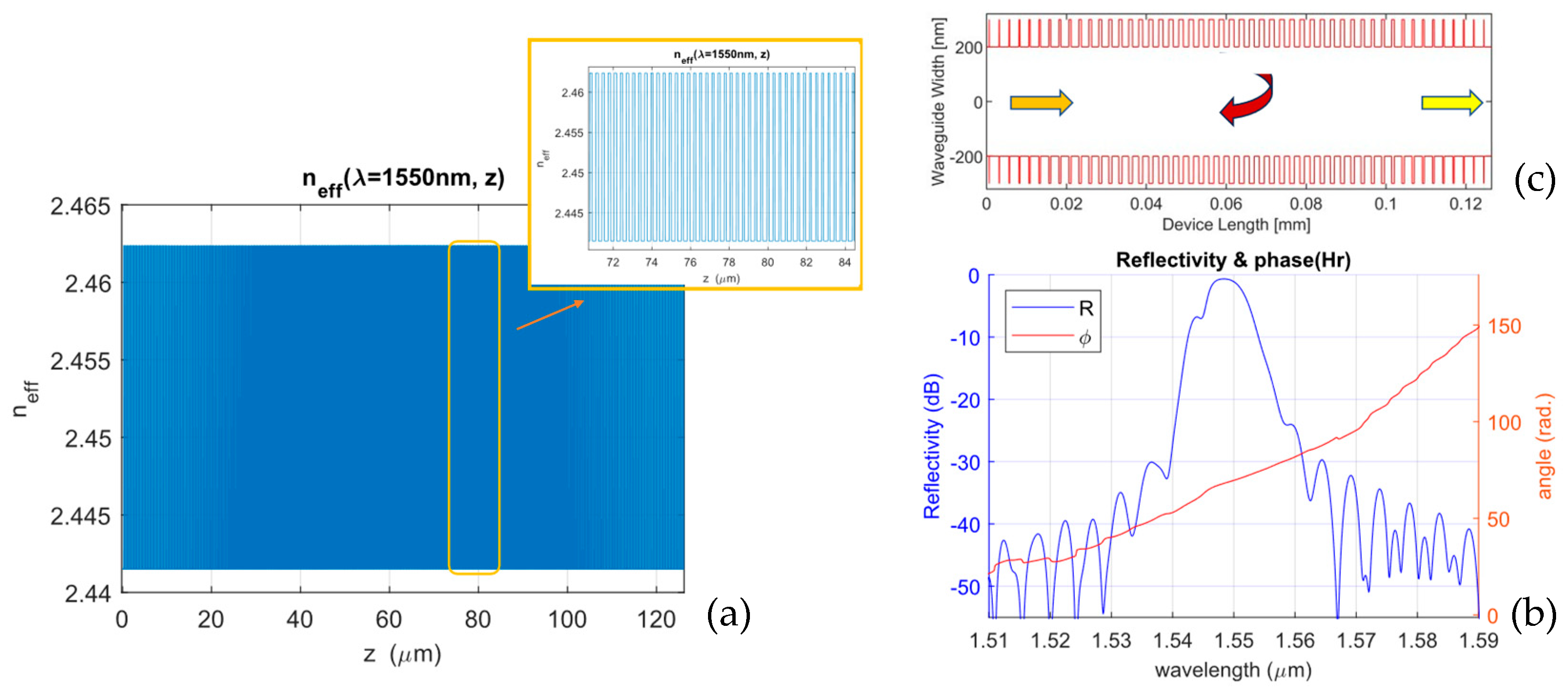
5.1. Apodization Through Corrugation Width Modulation

Given the relationship between neff and the width of the waveguide, the most straightforward method for apodizing the IBG is to modify its length along the x-axis (ΔW), mapping the apodization function A(z) onto the geometry of the grating (Figure 8a and Figure 9c) [44]. By introducing A(z) into (1) and setting φ(z) = 0 (no phase variation), the expression that defines the width of the grating becomes
W z = Δ W m a x square 2 π Λ B z · A ( z )
For a squared cosine apodization function, the obtained effective refractive index profile is shown in Figure 9a, along with the IBG spectrum reflectivity and phase resulting from applying the method (Figure 9b) and its geometrical structure (Figure 9c). It can be noted that there is no exact symmetry between the values above and below the neff(W0 = 500 nm); this effect is due to the non-linear variation in the effective refractive index with λ, which can cause variations in λB that must be accounted for.
As explained before, Figure 9a only can show the neff for a particular wavelength in the range [1500 nm, 1600 nm], in this case, for λB = 1550 nm. Note the effect of the apodization in the reduction of the side lobes in Figure 9b, which is precisely simulated by the ERI-TMM.

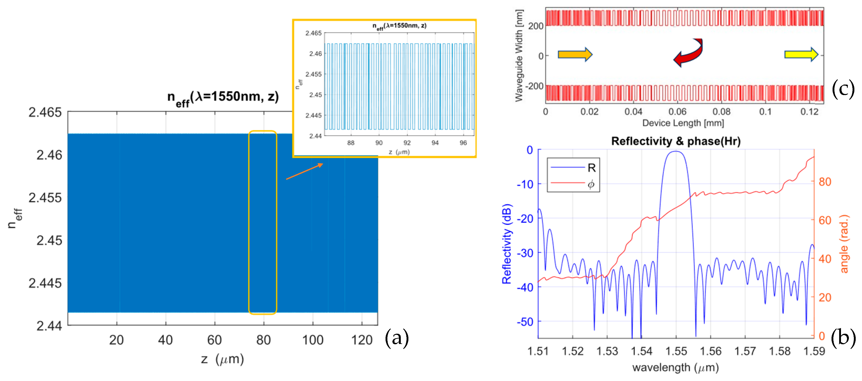
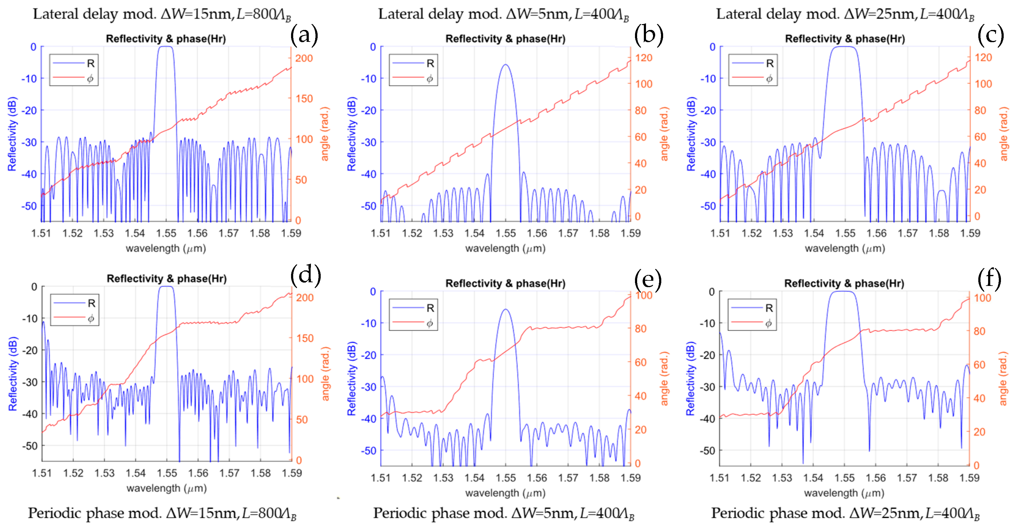
5.2. Apodization Through Lateral Delay Modulation

This technique consists of modifying the geometry of the grating by varying the offset Δφ between the functions that define the periodic geometric perturbation of the upper WU(z) and lower WL(z) parts of the IBG (Figure 8b and Figure 10c) [13,45,46]. In other words, a misalignment (ΔL) between the periods of the upper and lower edges of the waveguide is introduced. In this way, the corrugation width, ΔW, remains constant and equal to ΔWmax throughout the grating (e.g., for ΔW = 15 nm, the width is 485 or 515 nm for rectangular perturbation or has an amplitude of ±15 nm for sinusoidal perturbation), which avoids the variation of the average neff that light sees along the IBG, due to the non-linear variation that it undergoes with respect to ΔW, as explained above.
Thereby, in this case, the apodization is implemented through the spatial duration of each half-period of Bragg. Thus, in each Bragg period, for a given ΔW, the maximum apodization is achieved when the misalignment is zero (ΔL = 0, which corresponds to a phase shift Δφ = 0), and the minimum apodization occurs when the misalignment is maximum (ΔL = ΛB/2 which corresponds to a phase shift Δφ = π). This type of modulation allows for a more precise control of the apodization due to the cosine factor of the following equation, which expresses the relation between misalignment and apodization:
n = n 0 cos π L Λ B
where n0 is the effective refractive index of the unperturbed guide, neff(W0 = 500 nm). To implement a square cosine profile with this misalignment technique, Equation (21) is used, that is, n(z)→ΔL(z). The phase shift is then calculated, ΔL(z)→Δφ(z), which is finally introduced into (1) to define the geometry of the grating. In that way, the neff profile has been mapped in the geometry through the misalignment profile, while maintaining a constant perturbation width. The neff profile is plotted in Figure 10a.
This illustration is quite interesting because it gives an idea of the behavior of light. If we stick to it, light only sees three refractive indices in each Bragg half-period—neff,1(500 nm), neff,2(500 nm + ΔW), and neff,3(500 nm − ΔW)—but with a different length (Λi for each neff,i) for each half-period. Thus, in a sense, light averages the product neff,i·Λi in the first Bragg half-period to obtain an average neff,hp, the one that light sees, which can be expressed by
n e f f , h p = 2 Λ B i = 1 3 n e f f , i · Λ i
The same effect is generated in the second Bragg half-period, but symmetrically, so that the average neff remains constant throughout the Bragg period and therefore along the entire IBG, producing no chirp in λB. The reflectivity and phase of the reflection transfer function obtained via applying this modulation method are represented in Figure 10b.

5.3. Apodization Through Duty Cycle Modulation

In this technique, the neff profile is achieved by modifying the duty cycle of the periodic perturbation of the geometry (Figure 8c and Figure 11c) [47]. The duty cycle is defined as DC = h/ΛB, where h is the length of the corrugation in the z-dimension (or the positive Bragg half-period length) and 0 < h < ΛB/2. As in the previous method, the width of the perturbation ΔW remains constant along the IBG. The relationship between neff and DC is
n = n 0 sin π · D C
Thus, neff is modulated by the ratio between the corrugation length (z-dimension) and the Bragg period size. In this method, the sine factor provides better control of the apodization resolution than the perturbation modulation method. However, variations between the two Bragg half-periods affect the neff, resulting in variations in λB and hence in the transfer function. To implement a square cosine profile, relation (23) is used, that is, n(z)→DC(z). Then, the desired neff profile (Figure 11a) is mapped onto the geometry of the waveguide using (1) without changing the width of the perturbation.
Applying the model, the transfer function in reflection is obtained in Figure 11b. It can be seen that, in this case, the changes in the Bragg period do not keep the average neff constant. This has two effects: a distortion of the main lobe and an increase in the bandwidth (which indicates that there have been variations in λB and, therefore, an unwanted chirp has occurred). For this reason, this apodization method is only used with the simplest transfer functions, such as those that do not require control over the IBG phase geometry.

5.4. Apodization Through Periodic Phase Modulation

This method aims to modulate the effective refractive index of the grating by periodically modulating the phase of its geometry (Figure 8d and Figure 12c). It is similar to the apodization method of Section 5.2, but in this case, instead of modulating the phase difference between the upper and lower parts of the waveguide, the phase of both is varied simultaneously with a periodic function; see the function φ(z) in (1) and (2). This phase function (PF) can be sinusoidal, quadratic, triangular, or, in general, any other function, provided it is of a periodic nature. Better control of the apodization resolution is achieved on the basis of the ratio of the distance between adjacent corrugations to the Bragg period. A detailed description of this modulation technique, based on the theory of coupled modes, can be found in [48]. The proposed ERI-TMM modifies it to work, as in previous cases, with the effective refractive index, which allows us to consider any minimal variation in the geometry (and therefore in the neff). In this paper, a square phase function is chosen:
φ ( z ) = P ( z ) · square 2 π z Λ φ
Here, the amplitude P(z) translates the apodization function, in this case square cosine, into the geometry of the grating. The procedure is summarized as follows. First, the PF (which is periodic) is expanded into its complex exponential coefficients via the Fourier transform. In this way, each component represents a different Bragg order. The zero-order coefficient is the one that defines the first Bragg order, which is defined in (3) with m = 1. This is expressed as follows:
F 0 = 1 Λ φ 0 Λ φ e i φ ( z ) dz
where Λφ is the period of the PF. As explained in [48], F0 is proportional to the neff of the IBG, so F0 can be used to modulate the neff. Thus, substituting (24) into (25), F0 can be derived to be the following (for square PF):
F 0 = cos P z
Similarly, one can proceed to calculate the relationship between F0 and P(z) for any other periodic function.
Once P(z) is determined, the period Λφ must be chosen. This is a subtle issue because there is a trade-off between achieving a better spectral response (low values of Λφ) and complying with manufacturing restrictions (high values). The PF is then included in function (1), which governs the geometry of the IBG as the argument φ(z). The neff(z) profile obtained for the square cosine apodization is plotted in Figure 12a. Finally, the ERI-TMM is applied, and the reflectivity and phase of the transfer function in reflection are calculated (and represented in Figure 12b).

5.5. Comparison of Apodization Techniques Through ERI-TMM

The results obtained from the simulation are validated on the basis of a comparison of two of the apodization techniques and the alignment of the results of the ERI-TMM method with theoretical predictions. The analysis will focus on the lateral and periodic phase modulation methods, as they have proven to be the most efficient in achieving the desired transfer function and are also less sensitive to manufacturing constraints. The analysis involved modifying the width and length of the IBGs for both modulation methods to observe their impact on the spectral response. The results are presented in Figure 13, where the IBG characteristics are described in each plot. These results, along with those shown in Figure 9, Figure 10, Figure 11 and Figure 12, provide the following insights:
  • Reflectivity increases as predicted by theory for both longer lengths and greater corrugation widths [40].
  • The designed Bragg wavelength is maintained at 1550 nm, except for the duty-cycle technique due to the alterations introduced in the ΛB by this method [49].
  • The length of the IBG does not affect λB.
  • An increase in the IBG width results in a decrease in λB, due to the non-linear dependence shown in Figure 3c,d and Figure 4c,d.
  • The bandwidth increases as the corrugation width increases and decreases as the IBG length increases [27].

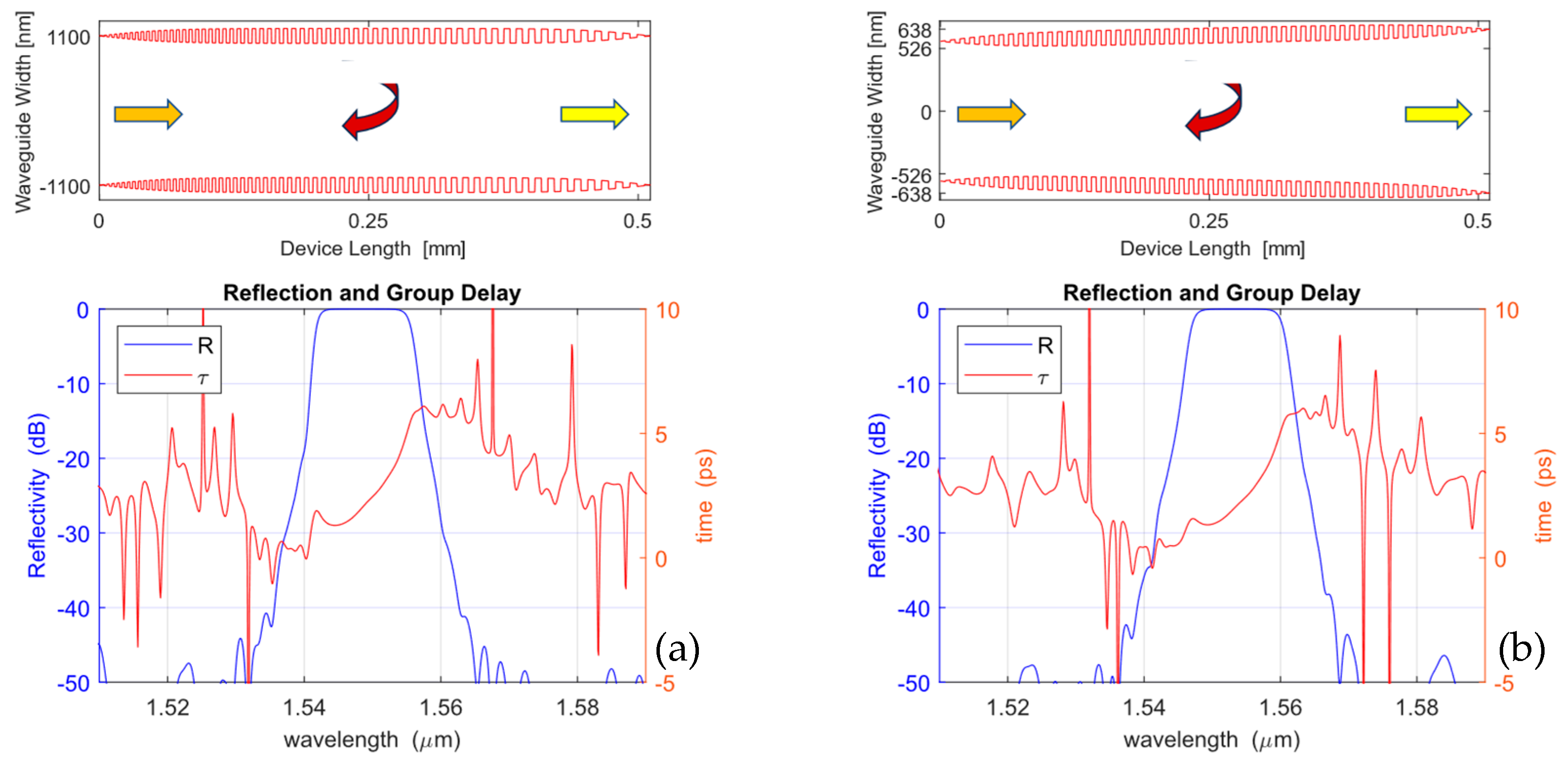
6. Advanced Simulation Results II: Chirp Techniques for an IBG

In IBG technology, chirp can be defined as the variation in the coupled Bragg wavelength along the grating. The aim is to achieve devices with a wider bandwidth that exhibit linear group delay in reflection. Traditionally, both objectives have been accomplished in FBGs by varying the Bragg period, allowing Bragg condition (3) to be fulfilled for multiple wavelengths along the waveguide. However, IBGs also allow us to modify the Bragg wavelength through variation in the average neff, as relation (3) also states. Thereby, there are two possible techniques to create a chirped IBG [50]:
  • Chirp via Bragg period variation. This method involves linearly changing the Bragg grating period along its length, causing a variation in λB and hence the bandwidth, which can be deduced from expression (3). The method keeps the waveguide width constant at W0. This variation can be mathematically expressed as follows:
    d λ B d z = 2 n e f f d Λ B d z
  • Chirp via IBG waveguide width variation. In this case, the method consists of linearly varying (increasing or decreasing) the average IBG width, W0(z), along the grating, to modify the neff, based on (7), and hence the λB. According to expression (3), this modification can be expressed as follows:
    d λ B d z = 2 Λ B d n e f f d z
By increasing or decreasing the average waveguide width and keeping the Bragg grating period ΛB constant, the desired chirp function is achieved.
The design process for a chirped IBG with specified parameters (bandwidth, group delay, reflectivity, and central wavelength) involves several steps that can be outlined as follows:
  • Calculating the Bragg grating period for the wavelengths of the spectral interval for the desired bandwidth using expression (3);
  • Using graphical representations or polynomial fits to determine the necessary waveguide width for a proposed effective refractive index at the wavelengths of interest;
  • Estimating the length of the IBG by evaluating the time it takes for the pulse to be reflected by the grating using the group index concept;
  • Applying the ERI-TMM method to obtain simulation results for reflectivity and group delay;
  • Fine-tuning the initial parameters to achieve a better transfer function if necessary, based on the obtained results.
The results of the modeling and simulation for both techniques are illustrated in Figure 14. In this case, the material is Al2O3, which shows good performance for applications in laser dispersion compensation [16], one of the application of chirped IBGs. Chirp via Bragg period variation is realized in a grating of W0 = 1100 nm with ΛB ranging from 506 nm to 512 nm, L = 1000ΛB, and ΔWmax = 100 nm. To improve the extinction ratio of the side lobes, a cosine squared apodization function is used (Figure 14a). Similarly, the simulation results for the second technique, chirp via IBG width variation, are plotted in Figure 14b. The chirped IBG is implemented in a grating with ΛB = 509 nm and a with a waveguide width varying from 1053 nm to 1276 nm; the IBG length L = 1000ΛB and ΔWmax = 100 nm.
As can be observed, both methods achieve similar results with appropriate parameter selection. In [50], a third method that combines both approaches is demonstrated, resulting in comparable spectra but with minor geometrical variation in the grating structure.

7. Advanced Simulation Results III: Complex IBG Profiles

This section explains and illustrates the results obtained by applying the ERI-TMM modeling and simulation process to more complex IBG apodizations. The objective is to develop tailored spectral responses that enable the design of optical devices that can be incorporated into PICs.

7.1. Phase Shifted IBG

It is common to introduce phase shifts in the neff profile to enable an IBG to work in transmission. Depending on the number of phase shifts and their position in the geometrical structure, it is possible to design a spectral response according to the desired specifications.
A common application of these IBGs is the design of very narrow filters in transmission. If a π-phase shift is introduced in the middle of the IBG apodization, a reflectivity spectrum as shown in Figure 15a,b is obtained, where the IBGs features are ΛB = 316 nm, L = 1000ΛB, W0 = 500 nm, and ΔWmax = 15 nm, clearly demonstrating a very narrow transmitted band and a π-phase shift at 1550 nm. Figure 15a implements this apodization profile with corrugation width delay modulation and a cosine square apodization function to reduce the side lobes. Figure 15b shows the equivalent spectral response for an IBG apodized through lateral delay modulation, also using a cosine square apodization function.
By adequately controlling the number of phase shifts and their positions within the IBG, the two lobes can be separated to achieve a two-passband filter with wide bandwidth and linear phase in the reflection spectral response, as shown in Figure 15c,d. These IBGs are implemented in a grating made with SOI technology, featuring ΛB = 316 nm, L = 400ΛB, and ΔWmax = 15 nm. The apodization is performed using a square cosine function through corrugation width modulation (Figure 15c) and lateral delay modulation (Figure 15d).

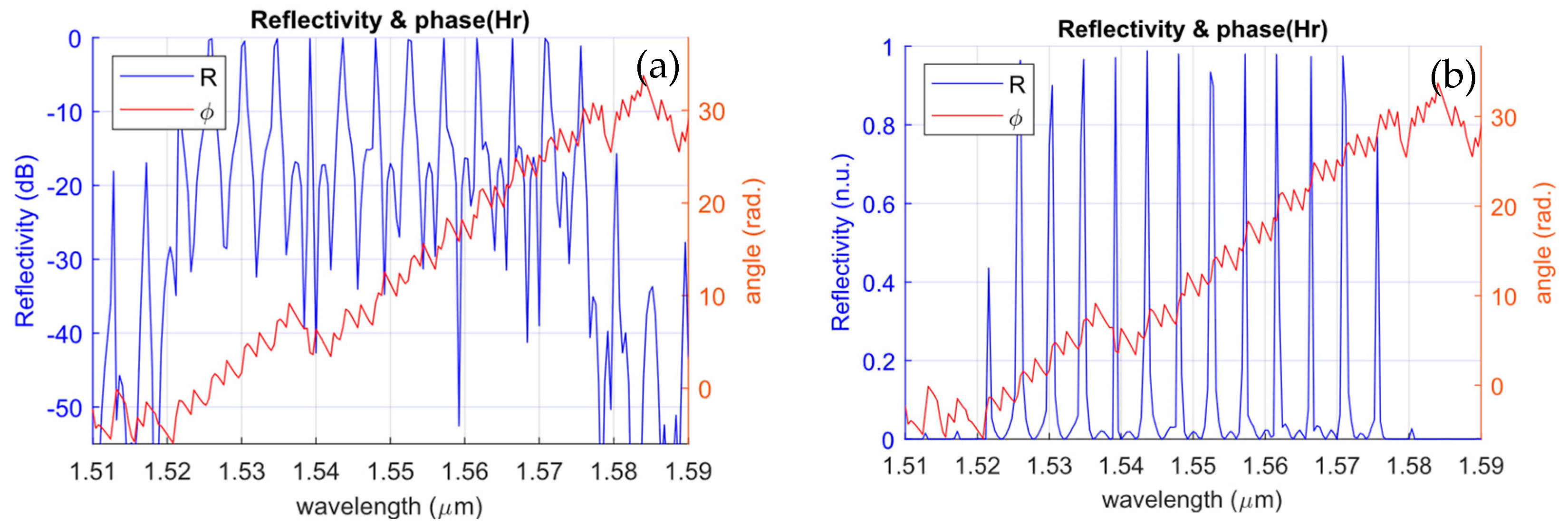
7.2. Sampled Diffraction Networks

The design and characterization of sampled diffraction gratings for use in multi-channel filtering in WDM optical communications systems is another application for IBGs. The IBG structure in SOI technology presented consists of 20 gratings with a sinc apodization function that is mapped onto the grating via the corrugation width modulation technique. Figure 16a shows the spectrum achieved after simulation, where a bandwidth of 0.5 nm (60 GHz), a channel separation of 3.5 nm (435 GHz), and a very high extinction ratio can be observed. In this case, the spectrum of the reflectivity in natural units (n.u.) is also plotted in Figure 16b for a better appreciation of the effect.

7.3. Hilbert Transformer

A Hilbert transformer (HT) is an important device in signal processing, with diverse applications in fields such as telecommunications, radar systems and image processing. In addition, a photonic HT can achieve significantly higher processing speeds compared to its electronic equivalent [13,51]. It is defined as a bandpass filter implementing a single discrete π-phase shift at the central wavelength in its phase spectral response. Two configurations are showed in Figure 17, both with ΛB = 316 nm, L = 1000ΛB, and ΔWmax = 15 nm. The design of Figure 17a uses corrugation width modulation, and the design of Figure 17b is achieved through lateral delay modulation.
Both results in Figure 17, despite incorporating very different geometries in the IBG, lead to similar spectra that clearly demonstrate the expected filter performance: high selectivity and attenuation outside the bandpass, flat frequency response and linear phase response within the passband, and a π-phase shift at the central wavelength.

8. Conclusions

The term “IBG spectral analysis” refers to the procedure to obtain the complete characterization of a given IBG working in a linear regime as a linear time-invariant system. In this sense, ERI–TMM is demonstrated as a powerful modeling and simulation approach to fully characterize IBGs. For this purpose, it is essential to characterize the waveguide to determine the effective refractive index as a function of wavelength and waveguide width. This method considers this double dependence; as Figure 7 confirms, if the wavelength dependence is not accounted for, the results do not agree with the experimental data.
The IBG analysis examples we performed demonstrate the ability of the proposed methodology to accurately map the geometric structure of the IBG onto the effective refractive index profile of the grating. The different obtained spectra show the following conclusions:
  • The validity of the method has been tested with experimental data for uniform IBG.
  • The bandwidth and intensity of the reflectivity respond to theoretical prediction and to experimental results.
  • Minimal differences in apodization can generate modifications in the spectral response, such as a single π-phase shift or several of them (Figure 15).
  • Different apodization techniques do not produce exactly the same spectral response, as can be observed in the sidelobes or in the Bragg wavelength (Figure 9, Figure 10, Figure 11, Figure 12 and Figure 13).
  • Variations in the Bragg period or waveguide width modify the Bragg wavelength (Figure 7 and Figure 14).
  • Increases in IBG length lead to a reduction in reflectivity bandwidth.
  • ERI-TMM can account for any physical variation in the geometry of the IBG and can translate it to the spectral response, to the order of 1 nm in the Bragg period. This can be verified by observing Figure 7, where the Bragg period is 317 nm to match the fabricated IBG. As can be seen, the Bragg wavelength of the simulated spectra is shifted to 1560 nm compared to the rest of the spectra in this paper, which are centered around 1550 nm due to a Bragg period of 316 nm, as stated by Equation (3).
  • This fine resolution ensures accurate representation of the grating features, providing reliable simulation results. The methodology has been demonstrated to be robust and versatile, making it suitable for a wide range of photonic applications.
  • Finally, the method also has proved to be capable of modeling both SOI and Al2O3 technologies.

Author Contributions

Conceptualization, J.Á.P. and A.C.; methodology, J.Á.P. and A.C.; software, J.Á.P.; validation, J.Á.P. and A.C.; formal analysis, J.Á.P. and A.C.; investigation, J.Á.P. and A.C.; resources, A.C.; writing—original draft preparation, J.Á.P.; writing—review and editing, J.Á.P. and A.C.; visualization, J.Á.P. and A.C.; project administration, A.C. All authors have read and agreed to the published version of the manuscript.

Funding

This research received no external funding.

Institutional Review Board Statement

Not applicable.

Informed Consent Statement

Not applicable.

Data Availability Statement

The original contributions presented in the study are included in the article. Further inquiries can be directed to the corresponding author.

Conflicts of Interest

The authors declare no conflicts of interest.

References

  1. Chrostowski, L.; Hochberg, M.E. Silicon Photonics Design; Cambridge University Press: Cambridge, UK, 2015; ISBN 978-1-107-08545-9. [Google Scholar]
  2. Reed, G.T.; Knights, A.P. Silicon Photonics: An Introduction; Wiley: Chichester, UK, 2005; ISBN 978-0-470-87034-1. [Google Scholar]
  3. Zhang, W.; Yang, S.; Zheng, S.; Wang, B. Low-Loss Ultra-Compact Silicon Photonic Integrated Micro-Disk Modulator for Large-Scale WDM Optical Interconnection. J. Light. Technol. 2024, 42, 3306–3313. [Google Scholar] [CrossRef]
  4. Sajan, S.C.; Singh, A.; Sharma, P.K.; Kumar, S. Silicon Photonics Biosensors for Cancer Cells Detection—A Review. IEEE Sens. J. 2023, 23, 3366–3377. [Google Scholar] [CrossRef]
  5. Dhote, C.; Singh, A.; Kumar, S. Silicon Photonics Sensors for Biophotonic Applications—A Review. IEEE Sens. J. 2022, 22, 18228–18239. [Google Scholar] [CrossRef]
  6. Chen, Y.; Lin, H.; Hu, J.; Li, M. Heterogeneously Integrated Silicon Photonics for the Mid-Infrared and Spectroscopic Sensing. ACS Nano 2014, 8, 6955–6961. [Google Scholar] [CrossRef] [PubMed]
  7. Liu, W.; Li, M.; Guzzon, R.S.; Norberg, E.J.; Parker, J.S.; Lu, M.; Coldren, L.A.; Yao, J. A Fully Reconfigurable Photonic Integrated Signal Processor. Nat. Photonics 2016, 10, 190–195. [Google Scholar] [CrossRef]
  8. Rivas, L.M.; Strain, M.J.; Duchesne, D.; Carballar, A.; Sorel, M.; Morandotti, R.; Azaña, J. Picosecond Linear Optical Pulse Shapers Based on Integrated Waveguide Bragg Gratings. Opt. Lett. 2008, 33, 2425. [Google Scholar] [CrossRef] [PubMed]
  9. Marpaung, D.; Yao, J.; Capmany, J. Integrated Microwave Photonics. Nat. Photonics 2019, 13, 80–90. [Google Scholar] [CrossRef]
  10. Iezekiel, S.; Burla, M.; Klamkin, J.; Marpaung, D.; Capmany, J. RF Engineering Meets Optoelectronics: Progress in Integrated Microwave Photonics. IEEE Microw. 2015, 16, 28–45. [Google Scholar] [CrossRef]
  11. Cheng, R. Spectral Tailoring of Silicon Integrated Bragg Gratings. Ph.D. Thesis, University of British Columbia, Vancouver, BC, Canada, 2020. [Google Scholar] [CrossRef]
  12. Wang, X. Silicon Photonic Waveguide Bragg Gratings. Ph.D. Thesis, University of British Columbia, Vancouver, BC, Canada, 2014. [Google Scholar] [CrossRef]
  13. Bazargani, H.P.; Burla, M.; Chrostowski, L.; Azaña, J. Photonic Hilbert Transformers Based on Laterally Apodized Integrated Waveguide Bragg Gratings on a SOI Wafer. Opt. Lett. 2016, 41, 5039. [Google Scholar] [CrossRef]
  14. Kulishov, M.; Azaña, J. Design of High-Order All-Optical Temporal Differentiators Based on Multiple-Phase-Shifted Fiber Bragg Gratings. Opt. Express 2007, 15, 6152. [Google Scholar] [CrossRef]
  15. Golovastikov, N.V.; Bykov, D.A.; Doskolovich, L.L.; Bezus, E.A. Spatial Optical Integrator Based on Phase-Shifted Bragg Gratings. Opt. Commun. 2015, 338, 457–460. [Google Scholar] [CrossRef]
  16. Sinobad, M.; Lorenzen, J.; Wang, K.; Dijkstra, M.; Gaafar, M.A.; Herr, T.; Garcia-Blanco, S.M.; Singh, N.; Kärtner, F.X. C-Band Apodized Chirped Gratings in Aluminum Oxide Strip Waveguides. In Proceedings of the European Conference on Integrated Optics, Enschede, The Netherlands, 19–21 April 2023. [Google Scholar]
  17. Simard, A.D.; Strain, M.J.; Meriggi, L.; Sorel, M.; LaRochelle, S. Bandpass Integrated Bragg Gratings in Silicon-on-Insulator with Well-Controlled Amplitude and Phase Responses. Opt. Lett. 2015, 40, 736. [Google Scholar] [CrossRef]
  18. Li, Y.; Xu, L.; Wang, D.; Huang, Q.; Zhang, C.; Zhang, X. Large Group Delay and Low Loss Optical Delay Line Based on Chirped Waveguide Bragg Gratings. Opt. Express 2023, 31, 4630. [Google Scholar] [CrossRef]
  19. Du, Z.; Xiang, C.; Fu, T.; Chen, M.; Yang, S.; Bowers, J.E.; Chen, H. Silicon Nitride Chirped Spiral Bragg Grating with Large Group Delay. APL Photonics 2020, 5, 101302. [Google Scholar] [CrossRef]
  20. Cheng, R.; Chrostowski, L. Spectral Design of Silicon Integrated Bragg Gratings: A Tutorial. J. Light. Technol. 2021, 39, 712–729. [Google Scholar] [CrossRef]
  21. Huang, W.-P. Coupled-Mode Theory for Optical Waveguides: An Overview. J. Opt. Soc. Am. A 1994, 11, 963. [Google Scholar] [CrossRef]
  22. Yariv, A. Coupled-Mode Theory for Guided-Wave Optics. IEEE J. Quantum Electron. 1973, 9, 919–933. [Google Scholar] [CrossRef]
  23. Kashyap, R. Fiber Bragg Gratings, 2nd ed.; Academic Press: Burlington, MA, USA, 2010; ISBN 978-0-12-372579-0. [Google Scholar]
  24. Othonos, A.; Kalli, K. Fiber Bragg Gratings: Fundamentals and Applications in Telecommunications and Sensing; Artech House optoelectronics library; Artech House: Boston, MA, USA, 1999; ISBN 978-0-89006-344-6. [Google Scholar]
  25. Skorobogatiy, M.; Johnson, S.G.; Jacobs, S.A.; Fink, Y. Dielectric Profile Variations in High-Index-Contrast Waveguides, Coupled Mode Theory, and Perturbation Expansions. Phys. Rev. E 2003, 67, 046613. [Google Scholar] [CrossRef]
  26. Sipe, J.E.; Poladian, L.; De Sterke, C.M. Propagation through Nonuniform Grating Structures. J. Opt. Soc. Am. A 1994, 11, 1307. [Google Scholar] [CrossRef]
  27. Carballar Rincón, A. Estudio de Redes de Difracción en Fibra Para su Aplicación en Comunicaciones Ópticas. Ph.D. Thesis, Universidad Politécnica de Madrid, Madrid, Spain, 1999. [Google Scholar]
  28. Fernández-Ruiz, M.R.; Carballar, A. Fiber Bragg Grating-Based Optical Signal Processing: Review and Survey. Appl. Sci. 2021, 11, 8189. [Google Scholar] [CrossRef]
  29. Macleod, H.A. Thin-Film Optical Filters, 5th ed.; Series in Optics and Optoelectronics; CRC Press/Taylor & Francis Group: Boca Raton, FL, USA, 2018; ISBN 978-1-138-19824-1. [Google Scholar]
  30. Kaushal, S.; Cheng, R.; Ma, M.; Mistry, A.; Burla, M.; Chrostowski, L.; Azaña, J. Optical Signal Processing Based on Silicon Photonics Waveguide Bragg Gratings: Review. Front. Optoelectron. 2018, 11, 163–188. [Google Scholar] [CrossRef]
  31. Reed, G.T. Silicon Photonics: The State of the Art; Wiley: Chichester, UK, 2008; ISBN 978-0-470-02579-6. [Google Scholar]
  32. Wörhoff, K.; Bradley, J.D.B.; Ay, F.; Pollnau, M. Low-Loss Al2O3 Waveguides for Active Integrated Optics. In Proceedings of the Conference on Lasers and Electro-Optics/Quantum Electronics and Laser Science Conference and Photonic Applications Systems Technologies, Baltimore, MD, USA, 6–11 May 2007; Optica Publishing Group: Washington, DC, USA, 2007; p. CMW5. [Google Scholar]
  33. West, G.N.; Loh, W.; Kharas, D.; Sorace-Agaskar, C.; Mehta, K.K.; Sage, J.; Chiaverini, J.; Ram, R.J. Low-Loss Integrated Photonics for the Blue and Ultraviolet Regime. APL Photonics 2019, 4, 026101. [Google Scholar] [CrossRef]
  34. Hendriks, W.A.P.M.; Chang, L.; Van Emmerik, C.I.; Mu, J.; De Goede, M.; Dijkstra, M.; Garcia-Blanco, S.M. Rare-Earth Ion Doped Al2O3 for Active Integrated Photonics. Adv. Phys. X 2021, 6, 1833753. [Google Scholar] [CrossRef]
  35. Lu, Z.; Jhoja, J.; Klein, J.; Wang, X.; Liu, A.; Flueckiger, J.; Pond, J.; Chrostowski, L. Performance Prediction for Silicon Photonics Integrated Circuits with Layout-Dependent Correlated Manufacturing Variability. Opt. Express 2017, 25, 9712. [Google Scholar] [CrossRef] [PubMed]
  36. Saleh, B.E.A.; Teich, M.C. Fundamentals of Photonics, 3rd ed.; Wiley Series in Pure and Applied Optics; Wiley: Hoboken, NJ, USA, 2019; ISBN 978-1-119-50687-4. [Google Scholar]
  37. Carballar, A.; Muriel, M.A. Growth Modeling of Fiber Gratings: A Numerical Investigation. Fiber Integr. Opt. 2002, 21, 451–463. [Google Scholar] [CrossRef]
  38. Yeh, P. Optical Waves in Layered Media; Wiley Series in Pure and Applied Optics; Wiley-Interscience: Hoboken, NJ, USA, 2005; ISBN 978-0-471-73192-4. [Google Scholar]
  39. Wang, X.; Yin, C.; Cao, Z. Progress in Planar Optical Waveguides; Springer Tracts in Modern Physics; Springer: Berlin/Heidelberg, Germany, 2016; Volume 266, ISBN 978-3-662-48982-6. [Google Scholar]
  40. Strain, M.J.; Sorel, M. Design and Fabrication of Integrated Chirped Bragg Gratings for On-Chip Dispersion Control. IEEE J. Quantum Electron. 2010, 46, 774–782. [Google Scholar] [CrossRef]
  41. Skaar, J.; Wang, L.; Erdogan, T. On the Synthesis of Fiber Bragg Gratings by Layer Peeling. IEEE J. Quantum Electron. 2001, 37, 165–173. [Google Scholar] [CrossRef]
  42. Lumerical. Copyright 2024 Ansys Canada Ltd. Available online: https://www.lumerical.com/ (accessed on 22 January 2024).
  43. Bojko, R.J.; Li, J.; He, L.; Baehr-Jones, T.; Hochberg, M.; Aida, Y. Electron Beam Lithography Writing Strategies for Low Loss, High Confinement Silicon Optical Waveguides. J. Vac. Sci. Technol. B 2011, 29, 06F309. [Google Scholar] [CrossRef]
  44. Murphy, T.E. Design, Fabrication and Measurement of Integrated Bragg Grating Optical Filters. Ph.D. Dissertation, Massachusetts Institute of Technology, Cambridge, MA, USA, 2001. [Google Scholar]
  45. Cheng, R.; Yun, H.; Lin, S.; Han, Y.; Chrostowski, L. Apodization Profile Amplification of Silicon Integrated Bragg Gratings through Lateral Phase Delays. Opt. Lett. 2019, 44, 435. [Google Scholar] [CrossRef]
  46. Jiang, W.; Feng, J.; Yuan, S.; Liu, H.; Yu, Z.; Yang, C.; Ren, W.; Xia, X.; Wang, Z.; Huang, F. Sidewall Corrugation-Modulated Phase-Apodized Silicon Grating Filter. Micromachines 2024, 15, 666. [Google Scholar] [CrossRef]
  47. Lupu, A. Duty Cycle Variation Methods for Bragg Gratings: Comparative Study and Optimal Design. J. Opt. Soc. Am. B 2021, 38, C175. [Google Scholar] [CrossRef]
  48. Cheng, R.; Chrostowski, L. Apodization of Silicon Integrated Bragg Gratings Through Periodic Phase Modulation. IEEE J. Sel. Top. Quantum Electron. 2020, 26, 8300315. [Google Scholar] [CrossRef]
  49. Cheng, R.; Han, Y.; Chrostowski, L. Characterization and Compensation of Apodization Phase Noise in Silicon Integrated Bragg Gratings. Opt. Express 2019, 27, 9516. [Google Scholar] [CrossRef] [PubMed]
  50. Praena, J.Á.; Carballar, A. Chirped Integrated Bragg Grating Design. Photonics 2024, 11, 476. [Google Scholar] [CrossRef]
  51. Burla, M.; Li, M.; Cortés, L.R.; Wang, X.; Fernández-Ruiz, M.R.; Chrostowski, L.; Azaña, J. Terahertz-Bandwidth Photonic Fractional Hilbert Transformer Based on a Phase-Shifted Waveguide Bragg Grating on Silicon. Opt. Lett. 2014, 39, 6241. [Google Scholar] [CrossRef]
Figure 1. (a) IBG geometries with rectangular and sinusoidal corrugations (features have been enlarged for the sake of illustration) for the specific case of a uniform IBG in SOI. (b) Simulated spectral power response in reflection. Orange arrow represents the co-directional field.
Photonics 12 00351 g001
Figure 2. (a) Relation between Bragg period and Bragg wavelength in an IBG (features enlarged for illustration). (b) Reflection phase shift at interfaces (red), transmission phase accumulated in layers (blue), providing n1 < n2. Orange and yellow arrows represent the co-directional fields while red arrows represent the contra-directional fields.
Photonics 12 00351 g002
Figure 3. SOI technology characterization for a strip waveguide. (a) Three-dimensional structure, with silicon in red and SiO2 in blue-grey. (b) Optical field intensity. (c) Obtained real and (d) imaginary part of the neff for different waveguide width values. The thicker red line represents neff(λ,W = 500 nm).
Photonics 12 00351 g003
Figure 4. Al2O3 technology characterization for a strip waveguide. (a) Three-dimensional structure, with Al2O3 in grey and SiO2 in light blue. (b) Optical field intensity. (c) Obtained real and (d) imaginary part of the neff for different waveguide width values. The thicker orange line represents neff(λ,W = 1100 nm).
Photonics 12 00351 g004
Figure 5. (a) Schematic representation of an apodized IBG, with the incoming (orange), co-directional (yellow), and contra-directional (red) fields. (b) Magnification (inside neff7) of three layers and two interfaces after the sampling process as well as the distribution of the fields within them. Orange and yellow arrows represent the co-directional fields while red arrows represent the contra-directional fields.
Photonics 12 00351 g005
Figure 6. (a) Illustration of a uniform IBG in SOI technology of length L and the relation of the fields. (b) Spectral response obtained after simulation for a square uniform IBG with L = 200ΛB and ΔW = 15 nm. Orange and yellow arrows represent the co-directional fields while red arrows represent the contra-directional fields.
Photonics 12 00351 g006
Figure 7. Simulated vs. experimental spectral response for a set of SOI-based uniform IBGs with ΛB = 317 nm: (a) rectangular perturbation, L = 200ΛB, ΔW = 10 nm; (b) rectangular, L = 400ΛB, ΔW = 10 nm; (c) sinusoidal, L = 200ΛB, ΔW = 10 nm; and (d) sinusoidal, L = 200ΛB, ΔW = 20 nm.
Photonics 12 00351 g007
Figure 8. Apodization methods: (a) Corrugation width modulation. (b) Lateral delay modulation. (c) Duty cycle modulation. (d) Phase delay modulation. (Features enlarged for illustration.)
Photonics 12 00351 g008
Figure 9. Square cosine apodized IBG in SOI technology with corrugation width modulation and rectangular perturbation; with ΛB = 316 nm, L = 400ΛB, and ΔWmax = 15 nm: (a) neff(λB = 1550 nm); (b) simulated spectrum; and (c) IBG structure (features enlarged for illustration).
Photonics 12 00351 g009
Figure 10. Square cosine apodized IBG with lateral delay modulation, with ΛB = 316 nm, L = 400ΛB, and ΔW = 15 nm: (a) neff(λB = 1550 nm) profile; (b) simulated spectrum; and (c) IBG structure (features enlarged for illustration).
Photonics 12 00351 g010
Figure 11. Square cosine apodized IBG with duty cycle modulation, with ΛB = 316 nm, L = 400ΛB, and ΔW = 15 nm: (a) neff(λB = 1550 nm) profile; (b) simulated spectrum; and (c) IBG structure (features enlarged for illustration).
Photonics 12 00351 g011
Figure 12. Square cosine apodized IBG with phase delay modulation, with ΛB = 316 nm, L = 400ΛB, and ΔW = 15 nm: (a) neff(λB = 1550 nm) profile; (b) simulated spectrum; and (c) IBG structure (features enlarged for illustration).
Photonics 12 00351 g012
Figure 13. Spectra of apodized IBGs designed with lateral and periodic phase modulation methods, with ΛB = 316 nm. (a) Lateral delay modulation (LDM) with ΔW = 15 nm, L = 800ΛB. (b) LDM with ΔW = 5 nm, L = 400ΛB. (c) LDM with ΔW = 25 nm, L = 400ΛB. (d) Phase delay modulation (PDM) with ΔW = 15 nm, L = 800ΛB. (e) PDM with ΔW = 5 nm, L = 400ΛB. (f) PDM with ΔW = 25 nm, L = 400ΛB.
Photonics 12 00351 g013
Figure 14. Apodized–chirped IBG in Al2O3 technology. Simulated spectrum for (a) chirped IBG via Bragg period variation, with 506 nm < ΛB < 512 nm, L = 1000ΛB, W0 = 1100 nm, and ΔWmax = 100 nm; (b) chirped IBG via width variation, with ΛB = 509 nm, L = 1000ΛB, 1053 nm < W0 < 1276 nm, and ΔWmax = 100 nm. The IBG structure for each is depicted at the top.
Photonics 12 00351 g014
Figure 15. Reflectivity and phase spectral responses for square cosine apodized IBGs in SOI technology with a π-phase shift in the periodical perturbation at the center of the grating: (a) corrugation width modulation; (b) lateral delay modulation. Apodized IBG with 15 π-phase shifts along the grating: (c) corrugation width modulation; (d) lateral delay modulation. All IBGs with ΛB = 316 nm, L = 400ΛB, and ΔWmax = 15 nm.
Photonics 12 00351 g015
Figure 16. Simulated spectrum for a sampled IBG in SOI technology with sinc apodization function via corrugation width modulation. IBG with ΛB = 316 nm, L = 4000 ΛB, ΔWmax = 15 nm, and rectangular perturbation. (a) Reflectivity in dB. (b) Reflectivity in natural units.
Photonics 12 00351 g016
Figure 17. Simulated spectrum for a photonic HT in SOI technology. (a) Corrugation width modulation. (b) Lateral delay modulation. IBG with ΛB = 316 nm, L = 1000ΛB, ΔWmax = 15 nm, and rectangular perturbation.
Photonics 12 00351 g017
Table 1. IBG typical geometrical parameters and values for SOI and Al2O3 technologies, working in the third optical communications window.
ParameterSOIAl2O3
W0 (x-dimension)500 nm1100 nm
H (y-dimension)220 nm400 nm
L (z-dimension)By designBy design
ΔWmax5–25 nm100–200 nm
ΔWmin≈6 nm
Lithography dependance
≈75 nm
Lithography dependance
ΛB~316 nm or ~317 nm~509 nm
λB1550 nm1550 nm
TypeStripStrip
CorrugationRectangularRectangular
Table 2. Common apodization functions.
Apodization FunctionMath Expression
Square (rise) cosine A z = c o s 2 π L z
Gaussian A z = exp z L / 2 2 2 σ 2
Sinc A z = sinc ( z L / 2 ) Λ a
Hyperbolic tangent A z = tanh 2 h z L , z < L / 2 t a n h 2 h ( L z ) L , z L / 2
Disclaimer/Publisher’s Note: The statements, opinions and data contained in all publications are solely those of the individual author(s) and contributor(s) and not of MDPI and/or the editor(s). MDPI and/or the editor(s) disclaim responsibility for any injury to people or property resulting from any ideas, methods, instructions or products referred to in the content.

