Communication

Performance Analysis of Chirped Graded Photonic Crystal Resonator for Biosensing Applications

1
Department of Electronics and Communication Engineering, Jaypee Institute of Information Technology, Noida 201309, India
2
Department of Electronics and Communication Engineering, Manipal Institute of Technology (MIT), Manipal Academy of Higher Education, Manipal 576104, India
*
Author to whom correspondence should be addressed.
Photonics 2024, 11(12), 1173; https://doi.org/10.3390/photonics11121173
Submission received: 30 October 2024 / Revised: 10 December 2024 / Accepted: 11 December 2024 / Published: 13 December 2024
(This article belongs to the Section Optical Interaction Science)

Abstract

:
In this manuscript, a chirped graded photonic crystal (PhC) resonator structure is optimized for biosensing applications. The proposed structure comprises a bilayer PhC with an aqueous defect layer, where the thickness grading within the material is introduced, considering alpha ( α ) as a grading parameter. The device performance is analytically evaluated using the finite element method (FEM). The impact of α , the resonator thickness, and the incidence angle on the device performance is analyzed. Further, the device’s ability to be used as a biosensor is evaluated, considering cholesterol as an analyte. The analytical results demonstrate an average sensitivity of 410 nm/RIU, a quality factor of 0.91 × 10 3 , and a figure of merit (FOM) of 2.47 × 10 2 RIU 1 , showing 88.5% and 43% improvements in sensitivity and FOM compared to recently reported devices. The device’s superior sensing performance makes it suitable for medical and commercial applications, while the use of thickness grading addresses fabrication limitations, offering a robust framework for advanced photonic device design.

1. Introduction

Photonic nanostructures have emerged as pivotal components in modern optics, enabling the precise manipulation of light at the nanoscale. With their periodic arrangement of materials possessing contrasting refractive indices, these structures provide superior control over the propagation of electromagnetic waves [1,2,3]. This widens their application in enhancing the photonic spin hall effect, tunable bandgap, sensors, radiative coolers, and filtering devices [4,5,6,7,8,9]. Among these numerous applications, biosensing has seen tremendous advancements due to photonic structures’ inherent ability to interact with light and biological materials at the nanoscale, resulting in highly sensitive and specific detection capabilities [10,11]. The performance of the conventional photonic crystal (PhC) structure is enhanced by introducing a defect layer, which disrupts the periodicity and alters the device’s dispersion characteristics. As a result, resonant modes are excited within the photonic bandgap (PBG). PhC resonators have shown immense potential in improving the device’s performance. This utilizes light confinement to amplify interactions between the optical fields and target analytes, enabling real-time, label-free detection [12,13].
Light–matter interactions can be further enhanced by considering grading in the optical thickness of the material. This utilizes both thickness grading and refractive index grading. The concept of optical thickness grading within PhC structures is a relatively recent advancement, aimed at controlling and manipulating light propagation by minimizing losses (scattering and reflection) for high-precision applications [14]. The optical thickness grading is attributed to refractive index grading or physical thickness grading. The graded index approach, in which the refractive index is gradually varied, helps reduce unwanted reflection and scattering, significantly improving sensitivity and overall performance [6,15,16,17]. Moreover, it offers flexibility in design, allowing for a substantial RI difference within the same material. The first graded structure comprising lattice constant grading was proposed by Centeno et al. [18]. Later, the concept was explored for various other applications. Recently, Savotchenko et al. proposed linear and parabolic index-graded photonic structures for wave-guiding applications [19]. Specifically for 1D PhC, these graded profiles (linear, exponential, and hyperbolic index grading) have initially been utilized for bandgap engineering [20,21] and later for biosensing applications [22,23]. Although index grading provides good results, achieving a precise and uniform gradient can be technically challenging, leading to fabrication inconsistencies that degrade the performance. Additionally, the graded structure may introduce scattering losses, especially at interfaces where the gradient is not smooth. Moreover, the design can be sensitive to wavelength variations, limiting the bandwidth of effective operation. Finally, the complexity of modeling and predicting the behavior of graded photonic crystals can complicate the design process, making it challenging to optimize for specific applications.
While most research on PhC structures has focused on refractive index-based grading, thickness grading also offers a different and equally powerful mechanism for controlling light–matter interactions. By tuning the thickness of each layer while keeping the refractive index fixed, one can achieve smoother transitions for light propagation without relying solely on material composition changes. The thickness grading or chirped graded structures allow for detailed control over the phase of the propagating light, providing better mode matching. This minimizes reflection and enhances light localization. These chirped structures create an inhomogeneous profile that can enhance light confinement and mode localization [15,16,17]. This is particularly advantageous in high-sensitivity applications, such as biosensing, where subtle changes in the effective optical path length can significantly improve the multi-analyte detection capability [6,24]. Numerous studies on chirped mirrors have focused on expanding the photonic bandgap, as this design allows for a wider reflection range [25,26,27]. This makes chirped mirrors particularly beneficial for applications requiring enhanced spectral performance. Additionally, thickness-graded photonic crystals are employed in solar cells to enhance light absorption by tailoring the structure to trap light more effectively. This optimization improves the overall efficiency in energy harvesting devices [28]. Therefore, chirped thickness-graded PhC structures have the potential to exhibit superior features that may be utilized to control the light–matter interactions and demonstrate their prospective uses to enhance sensitivity for low-concentration analyte detection. However, to the best of our knowledge, chirped thickness-graded PhC resonator structures have not been explored for biosensing applications.This approach holds significant potential for biosensing applications, particularly in enabling early detection for timely interventions and better patient outcomes. Further research and validation studies are required to thoroughly assess the capabilities of these techniques and facilitate their integration into clinical practice.
This paper analyzes the excitation of a resonating mode for a chirped graded PhC structure. The structure is designed with a bilayer PhC structure. The PhC resonator is formed by replacing the intermediate layer with an aqueous layer filled with a cholesterol analyte. The thickness grading is used to develop highly efficient nanophotonic resonators by systematically varying the bilayers’ physical thickness. A linear grading profile using alpha ( α ) as a grading parameter is considered for the analysis. The device performance analysis is carried out using the finite element method (FEM) in COMSOL Multiphysics. The impact of grading parameter variation on the excited resonating mode is analyzed. Detailed mode localization and determination of the electric field distribution within the chirped thickness-graded PhC resonator structure are carried out. Furthermore, the impact of the resonator thickness and incidence angle on the resonance wavelength is also studied in detail. Finally, the structure’s sensing performance is analytically assessed by considering cholesterol as a sensing analyte. The analytical results exhibit an average sensitivity of 410 nm/RIU, with an average FOM and quality factor of 2.47 × 10 2   RIU 1 and 0.91 × 10 3 , respectively. The proposed structure shows 88.5% higher sensitivity and 43% improvement in the FOM than recently reported values [29]. Ultimately, the device’s performance characteristics are compared with the most recent data in the literature, highlighting its advanced sensing capabilities for both medical and commercial applications. Additionally, this approach addresses the fabrication limitations of index grading and provides a more versatile framework for designing next-generation photonic devices with enhanced functionality.

2. Theoretical Analysis and Methods

The proposed chirped graded photonic resonator (CGR) structure is shown schematically in Figure 1. The structure comprises silicon as a high-index material and porous silicon (P-Si) as a low-index material. The porosity (Equation (2)) was considered to obtain the desired refractive index contrast, and the Sellmeier approximation was used to obtain the material refractive index (RI) [30]. The optical constant of the structure was tailored by utilizing thickness grading, which was introduced by considering alpha ( α ) as a grading parameter. This can be evaluated using Equation (1). The Si layer exhibited an increasingly chirped thickness grading characteristic, as shown in Figure 1a,c, whereas the P-Si exhibited decreasingly chirped thickness grading, as shown in Figure 1b,d. Here, the numbers 1, 2, 3, 4, and 5 represent the number of layers with chirped thickness grading utilizing the α factor. Figure 1e represents the final proposed structure, where the light is incident from the substrate side, and the portions of the reflected and transmitted wave are denoted by ‘R’ and ‘T’, respectively. The final proposed structure was configured as [Substrate ∣ ( n HA , n LA ) 3 ∣ defect, ∣ ( n LA , n HA ) 3 ∣ Air], with a step-index low ( n LA ) and high ( n HA ) RI of 1.6 (80% porosity) and 3.45 (0% porosity), respectively. The initial defect layer parameters (thickness and RI) were considered to be similar to those of the higher index layer. A layer’s porosity (P) can be analytically calculated using Equation (2) [31].
d i + 1 = ( 1 + α ) × d i .
P = ( n p 2 n d s 2 ) ( n a 2 2 n d s 2 ) ( n p 2 + 2 n d s 2 ) ( n a 2 n d s 2 ) .
Here, d i and d i + 1 represent the thickness of two consecutive layers (‘A’ or ‘B’). In this context, ‘i’ corresponds to the first layer. In Equation (2), the refractive indices n p , n ds , and n a represent the refractive indices of the porous silicon, dense silicon, and air/analyte, respectively.
The structural performance is evaluated using the finite element method (FEM). Initially, a normal PhC structure (without grading) is considered for analysis, and the results are demonstrated in Figure 2a. The structure exhibits a photonic bandgap (PBG) of around 1207–2130 nm for the high and low index layer thicknesses d A and d B of around 112 nm and 242 nm, respectively. The thickness values are determined using a quarter-wave Bragg stack configuration with a central wavelength of 1550 nm. Furthermore, the resonance behavior of the structure is achieved by infiltrating the defect layer with the cholesterol analyte at a concentration of 200 mg/dL (with the normal concentration range having an RI of 2.49). This leads to the sharp resonance peaks of around 1951 nm with a full-width-half-maximum (FWHM) of around 2.50 nm, as shown in Figure 2a. This provides a Q factor of around Q = n o n g r a d e d 0.78 × 10 3 . The introduction of grading will impact the optical thickness and, hence, the reflectance behavior of the devices. Thus, this study is expanded to examine how the proposed structure is affected by chirped thickness grading.

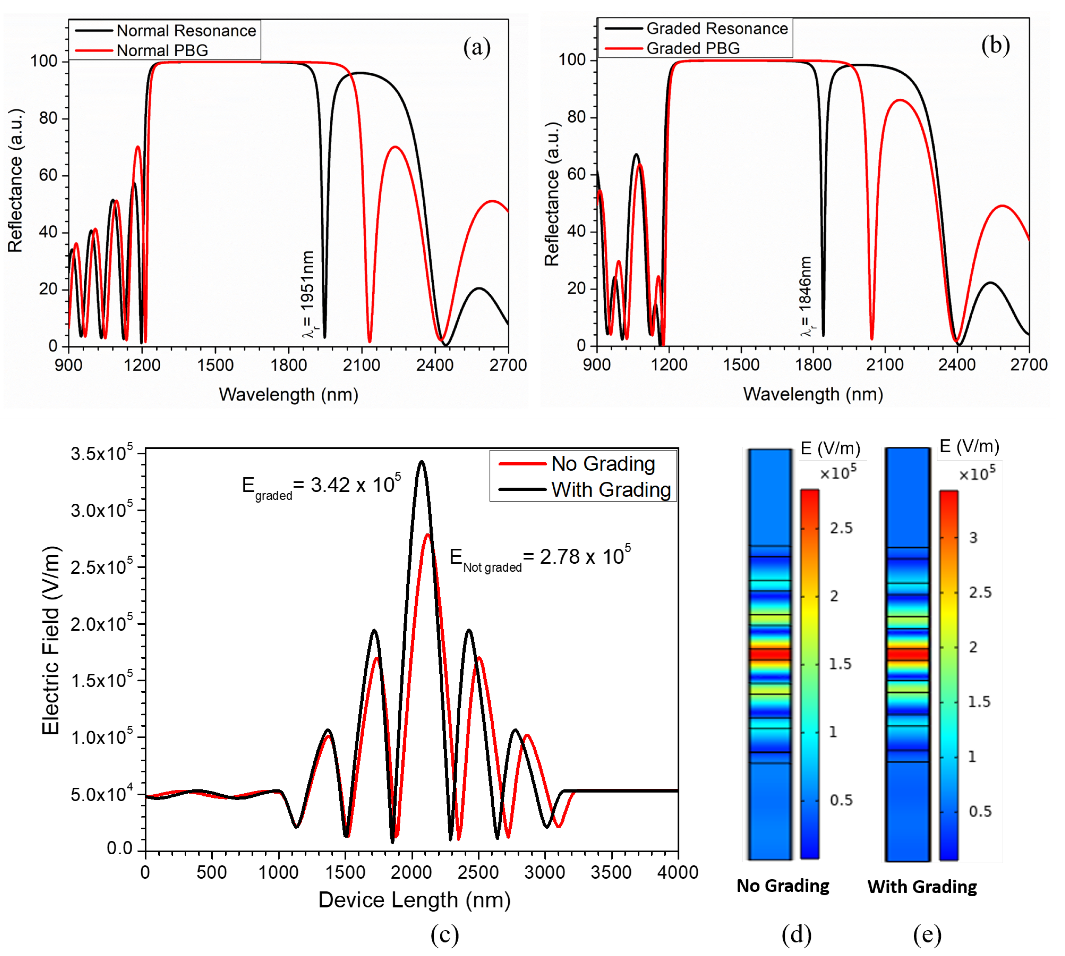
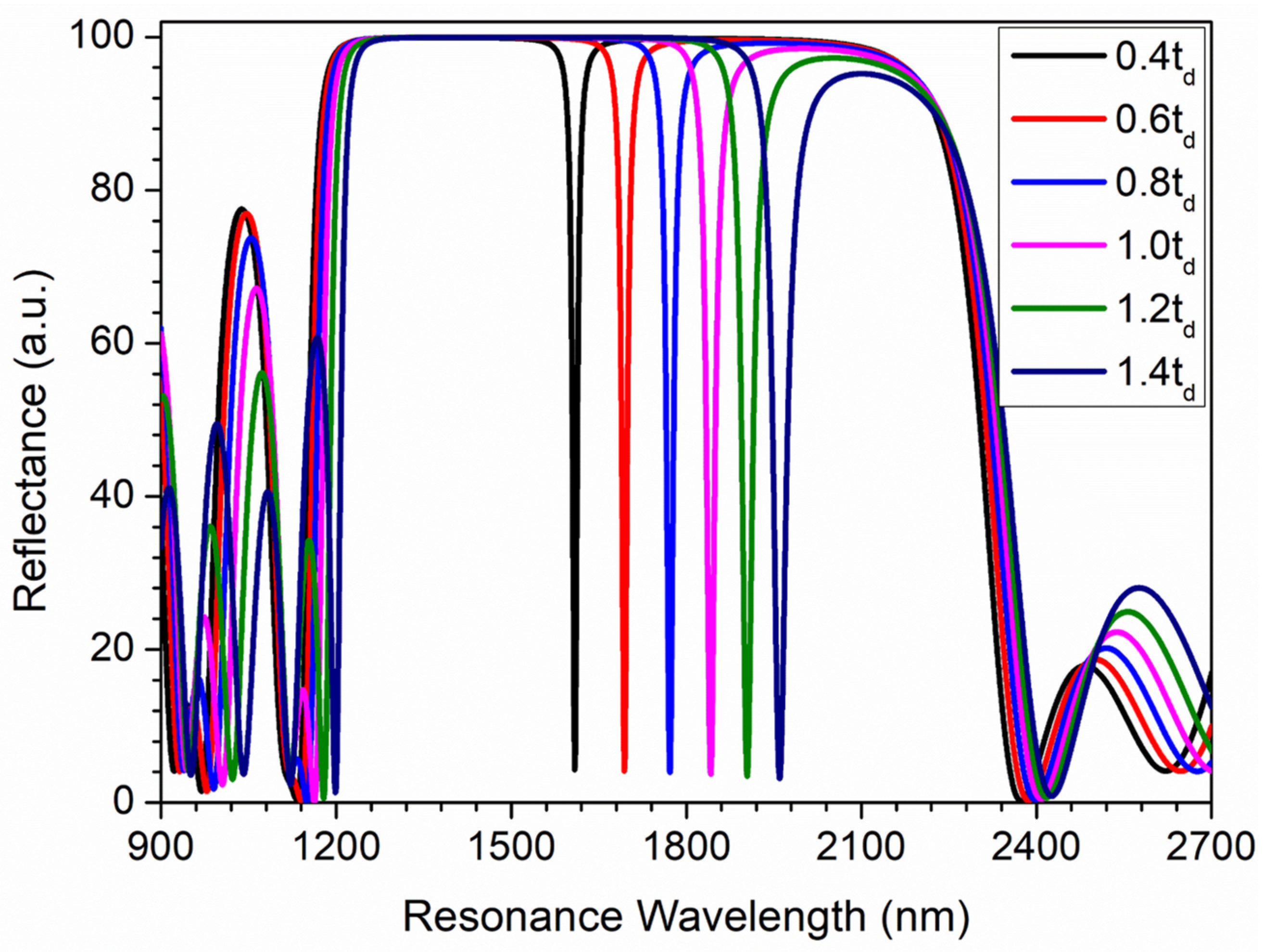
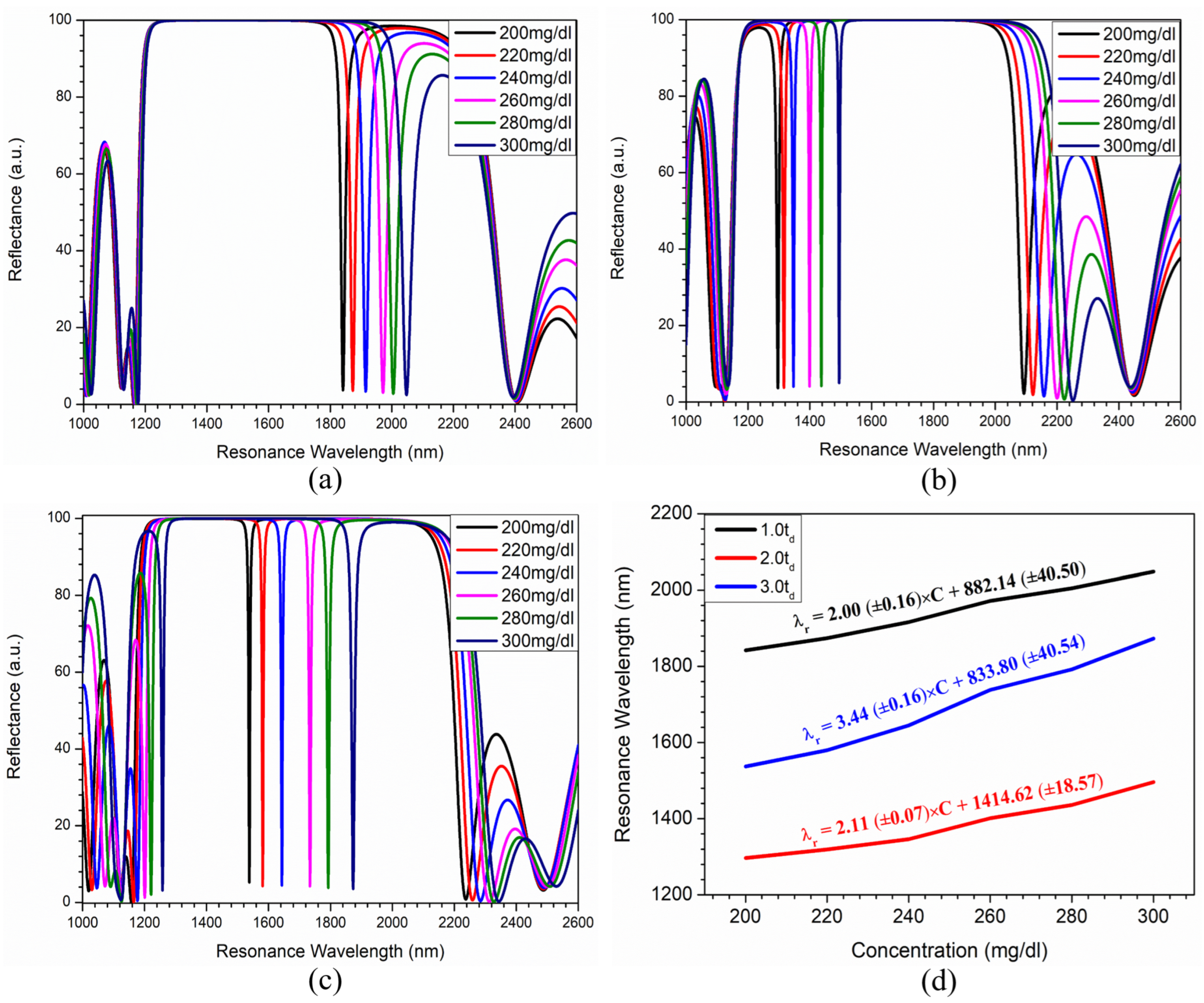
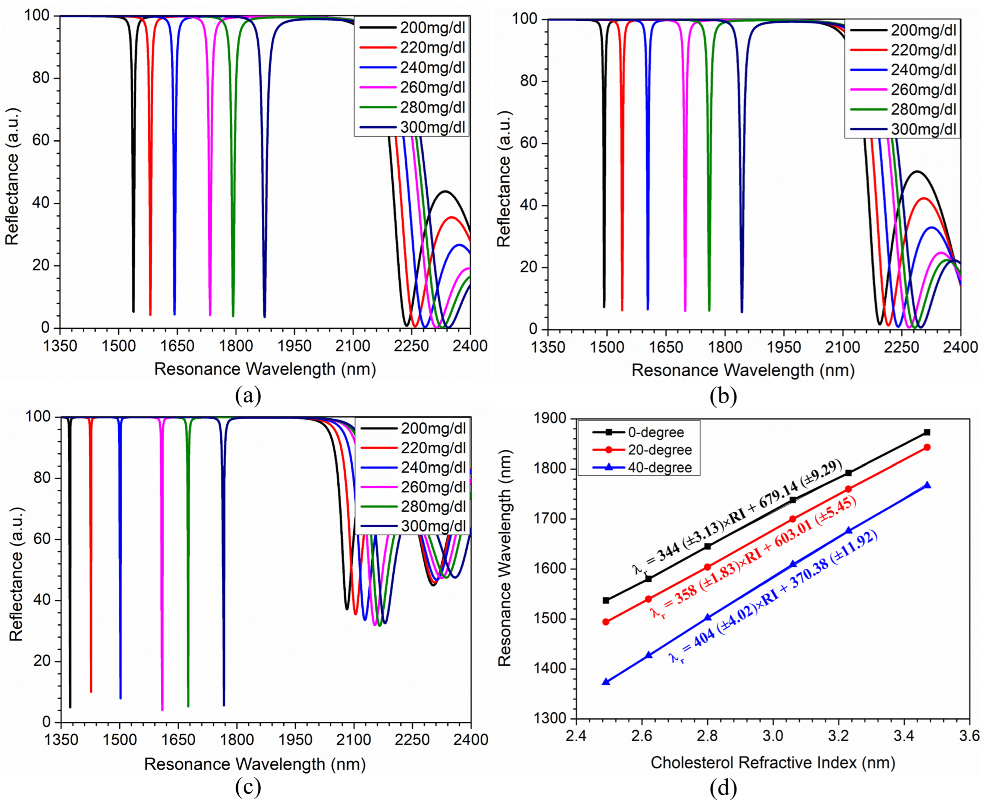
3. Results and Discussion

Chirped thickness grading was introduced to retain the device reflectance characteristics, as shown in Figure 1e. Here, A1, A2, and A3 and B1, B2, and B3 represent the graded high and low index layers. Figure 2b shows the reflectance response of the CGR structure with 4 nm grading ( α = 3.5%) in layer ‘A’ and −20 nm grading ( α = −8.26%) in layer ‘B’. This gives d A 1 , d A 2 , and d A 3 and d B 1 , d B 2 , and d B 3 values of around 112 nm, 116 nm, and 120 nm and 242 nm, 222 nm, and 202 nm, respectively. This exhibits a photonic PBG of around 1170–2040 nm. Furthermore, the CG-structure shows a superior excitation of the resonating mode for the infiltrated cholesterol analyte at a concentration of 200 mg/dL, which leads to sharp resonance peaks of around 1846 nm with an FWHM of around 2.02 nm, as shown in Figure 2b. This provides a Q factor of around Q = g r a d e d 0.91 × 10 3 , which is 16% higher than that of the corresponding normal PhC resonator structure. Further, the impact of a chirped graded profile on the electric field distribution for both structures was evaluated and is presented in Figure 2c. The chirped graded PhC resonator structure exhibits a resonating surface electric field intensity of around E = g r a d e d 3.42 × 10 5 V/m, which is 23% higher than that of the corresponding normal PhC resonator structure. The three-dimensional (3D) electric field distribution for both non-graded and graded structures is shown in Figure 2d,e. The excited resonance mode is highly susceptible to variations in the infiltrated analyte and chirped grading parameter ( α ). Thus, first, the impact of α variation was evaluated. The α was uniformly varied from −4% to +4%, and the reflectance results are presented in Figure 3a. Decreasing the α results in the excitation of a higher-energy resonating mode.
Figure 3b shows the impact of graded parameter variation on the resonance wavelength. The structure exhibits excitation of the resonating mode at resonance wavelengths of 1828 nm, 1870 nm, 1936 nm, 1956 nm, and 2000 nm under α variation of −4%, −2%, 0%, 2%, and 4%, respectively. The α -dependent resonance wavelength can be calculated using Equation (3).
λ r ( n m ) = 22.51 ( ± 0.82 ) × α + 1918.36 ( ± 2.59 )
Further, the effect of the PhC resonator thickness on the excited resonating mode for the proposed CGR structure was evaluated, and the results are described in Figure 4. The structure demonstrated excitation of a higher-energy resonating mode with a much narrower FWHM when decreasing the defect layer thickness. The CG structure showed resonating mode excitation at 1609 nm, 1694 nm, 1772 nm, 1843 nm, 1904 nm, and 1960 nm operating wavelengths for defect layer thicknesses of 0.4 t d , 0.6 t d , 0.8 t d , 1.0 t d , 1.2 t d , and 1.4 t d , respectively. It is worth mentioning that increasing the defect layer thickness further excites lower-energy resonating modes, with similar variations in operating wavelength ( d λ d t d ). This results in the additional advantage of enhanced light–matter interaction, improving the sensitivity.

Sensing Analysis

The device’s sensing performance was assessed by infiltrating the defect layer with analytes of varying cholesterol concentrations. The effects of different analyte concentrations and defect layer thicknesses on the resonating wavelengths were examined. Introducing porosity allows analytes to infiltrate the defect layer, modifying the effective refractive index (RI), which in turn causes a shift in the resonating wavelength of the excited mode. The refractive index values of the analyte at various cholesterol concentrations are listed in Table 1 [32].
Any sensor’s performance is measured in terms of certain parameters, like sensitivity (S), sensor resolution (SR), signal-to-noise ratio (SNR), detection limit (DL), and figure of merit (FOM). These parameters can be evaluated using Equations (4)–(8).
S = Δ λ Δ n .
F O M = S F W H M .
S N R = Δ λ r F W H M .
S R = F W H M 1.5 × ( S N R ) 0.25 .
D L = S R S .
where the sensitivity ‘S’ is determined as a ratio of the resonant peak position ( Δ λ ) to the resonant peak of the normal cell ( λ h i g h c h o l e s t e r o l λ n o r m a l c h o l e s t e r o l ), and Δ n denotes the difference in refractive indices between the sensing cholesterol concentration and the normal cholesterol concentration ( n h i g h c h o l e s t e r o l n n o r m a l c h o l e s t e r o l ). The figure of merit (FOM) can be evaluated as the ratio of sensitivity to the FWHM, as expressed in Equation (5), where the FWHM is the spectral half-width of the resonant wavelength dip. The signal-to-noise ratio (SNR), another important parameter, can be evaluated using Equation (6), where Δ λ r indicates the shift in the resonant wavelength. The sensor resolution (SR) is the smallest spectral shift that can be detected and is calculated using Equation (7). The detection limit is the smallest change in refractive index that the sensor can detect, and it is calculated by dividing the sensor resolution by the sensitivity [33,34].
The device’s sensing performance was compared for different defect layer thicknesses from 1.0 t d to 3.0 t d . Figure 5a shows the reflectance response of the proposed structure at a defect layer thickness of 1.0 t d for different cholesterol concentrations (infiltrated analytes), including 200 mg/dL (the normal cholesterol concentration with an RI of 2.49), 220 mg/dL (RI 2.62), 240 mg/dL (RI 2.8), 260 mg/dL (RI 3.06), 280 mg/dL (RI 3.23), and 300 mg/dL (RI 3.47) at a normal incidence angle. This study also investigated the effect of defect layer thicknesses of 2.0 t d and 3.0 t d on the sensor’s performance, and the results are shown in Figure 5b,c. The comparative analysis is shown in Figure 5d. When the analyte infiltrates the defect layer, its effective index increases, which causes the redshift of the resonating wavelength. The shift in resonance wavelength for a given resonator layer thickness can be calculated using Equations (9) and (10). This shows a sensitivity of around 2 nm/(mg/dL), 2.11 nm/(mg/dL), and 3.44 nm/(mg/dL) for 1.0 t d , 2.0 t d , and 3.0 t d defect layer thicknesses at a 0-degree incidence angle. It was observed that the sensitivity of the sensor with a 3.0 t d defect layer thickness was 70% higher than that of the normal structure.
λ r t d ( n m ) = 2.00 ( ± 0.16 ) × C + 882.14 ( ± 40.50 )
λ r 2 t d ( n m ) = 2.11 ( ± 0.07 ) × C + 1414.62 ( ± 18.57 )
λ r 3 t d ( n m ) = 3.44 ( ± 0.16 ) × C + 883.80 ( ± 40.54 )
Here, λ r represents the resonance wavelength in ‘nm’, and ‘C’ is the cholesterol concentration in ‘mg/dL’. The results show that the sensor’s performance can be improved by optimizing the defect layer thickness. The structural performance parameters and corresponding comparative results of the CG resonator structure are summarized in Table 2.
The sensitivity can be further enhanced by changing the incidence angle. The following section describes how the defect layer’s thickness affects the sensor’s performance at different angles of incidence. The sensitivity of the sensor increased with the angle of incidence for a given defect layer thickness due to increased light–matter interaction. The device’s sensing performance was compared at different angles of incidence (0 degrees, 20 degrees, and 40 degrees) for a defect layer thickness of 3.0 t d . The sensitivity response of the proposed chirped thickness graded resonator for a 3.0 t d defect layer thickness at varying incidence angles is shown in Figure 6. The 3.0 t d defect layer thickness shows narrow reflectance peaks, which become narrower at a 40-degree incidence angle.
λ r 0 d e g r e e ( n m ) = 344 ( ± 3.13 ) × R I + 679.14 ( ± 9.29 )
λ r 20 d e g r e e ( n m ) = 358 ( ± 1.83 ) × R I + 603.01 ( ± 5.45 )
λ r 40 d e g r e e ( n m ) = 404 ( ± 4.02 ) × R I + 370.38 ( ± 11.92 )
Here λ r represents the resonance wavelength in ‘nm’, and ‘RI’ is the corresponding refractive index of the cholesterol concentration given in Table 1. The CCG resonator shows average sensitivities of around 344 nm/RIU, 358 nm/RIU, and 404 nm/RIU for corresponding incidence angles of 0 degrees (shown in Figure 6a), 20 degrees (shown in Figure 6b), and 40 degrees (shown in Figure 6c), respectively, and the comparative analysis is shown in Figure 6d. Equations (12)–(14) can be utilized to calculate the cholesterol analyte’s RI-dependent resonance wavelength shift. The structure exhibited an average sensitivity and high quality factor of around 404 nm/RIU and 0.91 × 10 3 , respectively. This shows an average FOM of around 247 RIU 1 .
The obtained average FOM and sensitivity values were 43% and 88.5%, which are better than recently reported values [29]. Thus, the proposed CG resonator structure demonstrates its potential applicability to be used as a refractive-index-based biosensor. The sensing performance of the chirped thickness graded PhC resonator structure using a 3.0 t d defect layer thickness at 0-degree, 20-degree, and 40-degree incidence angles is summarized in Table 3. Finally, the structural performance compared with recent results is reported in Table 4. The proposed biosensor significantly outperforms existing biosensing research in terms of the average sensitivity, figure of merit, and quality factor, as demonstrated in Table 4 [29,35,36,37,38].

4. Conclusions

This study analyzes a chirped graded photonic crystal (PhC) resonator structure that has been optimized through systematic thickness grading for enhanced performance. By employing a linear grading profile with the grading parameter ( α ), the proposed structure exhibits superior resonance behavior. The introduction of chirped thickness grading enables precise control over the device’s optical properties. The infiltration of cholesterol as a sensing analyte highlights the potential of the structure in biosensing applications. The device demonstrates an impressive sensitivity of 410 nm/RIU and an FOM of 2.47 × 10 2 RIU 1 . The proposed device’s versatility, ease of fabrication, and robust performance make it highly suitable for medical and commercial sensing applications. The incorporation of thickness grading provides a promising pathway for designing next-generation photonic devices with improved functionality and fabrication feasibility.

Author Contributions

Conceptualization, A.K.G., A.K. and J.S.; Formal analysis, J.S. and A.K.; Investigation, A.K.G.; Methodology, A.K.G., A.K. and J.S.; Validation, A.K. and J.S.; Writing—original draft, A.K.G., A.K. and J.S.; Writing—review and editing, A.K. and J.S. All authors have read and agreed to the published version of the manuscript.

Funding

This research received no external funding.

Institutional Review Board Statement

Not applicable.

Informed Consent Statement

Not applicable.

Data Availability Statement

Data supporting the results presented in this paper are not publicly available at this time but may be obtained from the authors upon reasonable request.

Conflicts of Interest

The authors declare no conflicts of interest.

References

  1. Joannopoulos, J.D.; Johnson, S.G.; Winn, J.N.; Meade, R.D. Photonic Crystals: Molding the Flow of Light; Princeton University Press: Princeton, NJ, USA, 2008. [Google Scholar]
  2. Fink, Y.; Winn, J.N.; Fan, S.; Chen, C.; Michel, J.; Joannopoulos, J.D.; Thomas, E.L. A dielectric omnidirectional reflector. Science 1998, 282, 1679–1682. [Google Scholar] [CrossRef] [PubMed]
  3. Winn, J.N.; Fink, Y.; Fan, S.; Joannopoulos, J.D. Omnidirectional reflection from a one-dimensional photonic crystal. Opt. Lett. 1998, 23, 1573–1575. [Google Scholar] [CrossRef] [PubMed]
  4. Goyal, A.K.; Divyanshu, D.; Massoud, Y. Excitation of optical tamm state for photonic spin hall enhancement. Sci. Rep. 2024, 14, 175. [Google Scholar] [CrossRef] [PubMed]
  5. Ratra, K.; Singh, M.; Goyal, A.K. Design and Analysis of Omni-directional Solar Spectrum Reflector using One-dimensional Photonic Crystal. J. Nanophotonics 2020, 14, 026005. [Google Scholar] [CrossRef]
  6. Goyal, A.K.; Dutta, H.S.; Pal, S. Porous photonic crystal structure for sensing applications. J. Nanophotonics 2018, 12, 040501. [Google Scholar] [CrossRef]
  7. Wu, F.; Chen, M.; Xiao, S. Wide-angle polarization selectivity based on anomalous defect mode in photonic crystal containing hyperbolic metamaterials. Opt. Lett. 2022, 47, 2153–2156. [Google Scholar] [CrossRef]
  8. She, Y.; Liu, D.; Li, J.; Yao, M.; Zheng, Y.; Wu, F. Tunable wide-angle high-efficiency polarization selectivity based on a one-dimensional photonic crystal containing elliptical metamaterials. Phys. Lett. A 2024, 494, 129299. [Google Scholar] [CrossRef]
  9. Goyal, A.K.; Divyanshu, D.; Massoud, Y. Nanophotonic resonator assisted photonic spin Hall enhancement for sensing application. Sci. Rep. 2023, 13, 9292. [Google Scholar] [CrossRef]
  10. Fan, X.; White, I.M. Optofluidic Microsystems for Chemical and Biological Analysis. Nat. Photonics 2011, 5, 591–597. [Google Scholar] [CrossRef]
  11. Vollmer, F.; Arnold, S. Whispering-Gallery-Mode Biosensing: Label-Free Detection Down to Single Molecules. Nat. Methods 2008, 5, 591–596. [Google Scholar] [CrossRef]
  12. Jokar, M.H.; Naraghi, A.; Seifouri, M.; Olyaee, S. Photonic crystal bio-sensor for highly sensitive label-free detection of cancer cells. Opt. Quantum Electron. 2023, 55, 660. [Google Scholar] [CrossRef]
  13. Fatemeh, B.; Samaneh, H. Label-Free cancer cell biosensor based on photonic crystal ring resonator. Results Phys. 2023, 46, 2211–3797. [Google Scholar]
  14. Gangwar, R.K.; Pathak, A.K.; Kumar, S. Recent Progress in Photonic Crystal Devices and Their Applications: A Review. Photonics 2023, 10, 1199. [Google Scholar] [CrossRef]
  15. Kurt, H.; Citrin, D.S. Graded index photonic crystals. Opt. Express 2023, 15, 1240–1253. [Google Scholar] [CrossRef] [PubMed]
  16. Das, D.; Saini, J.; Goyal, A.K.; Massoud, Y. Exponentially index modulated nanophotonic resonator for high-performance sensing applications. Sci. Rep. 2023, 13, 1431. [Google Scholar]
  17. Dash, D.; Saini, J. Linearly Graded Photonic Crystal with Improved Sensitivity for Sensing Application. In Proceedings of the 2022 8th International Conference on Signal Processing and Communication (ICSC), Noida, India, 1–3 December 2022; pp. 144–146. [Google Scholar]
  18. Centeno, E.; Cassagne, D. Graded photonic crystals. Opt. Lett 2005, 30, 2278–2280. [Google Scholar] [CrossRef]
  19. Savotchenko, S.E. Temperature-controlled waveguide properties of the linearly graded-index film in the photorefractive crystal. Appl. Phys. B 2023, 129, 7. [Google Scholar] [CrossRef]
  20. Rauh, H.; Yampolskaya, G.I.; Yampolskii, S.V. Optical transmittance of photonic structures with logarithmically similar dielectric constituents. J. Opt. 2012, 14, 015101. [Google Scholar] [CrossRef]
  21. Singh, B.K.; Bambole, V.; Rastogi, V.; Pandey, P.C. Multi-channel photonic bandgap engineering in hyperbolic graded index materials embedded one-dimensional photonic crystals. Opt. Laser Technol. 2020, 129, 106293. [Google Scholar] [CrossRef]
  22. Goyal, A.K.; Dash, D.; Saini, J.; Massoud, Y. Theoretical analysis of graded-index topological resonator for improved sensing performance. Opt. Express 2024, 32, 4102–4110. [Google Scholar] [CrossRef]
  23. Savotchenko, S.E. Features of the surface wave propagation along the interface between the hyperbolic graded-index layer and nonlinear medium with a step change in the dielectric constant. Phys. Lett. A 2024, 524, 129822. [Google Scholar] [CrossRef]
  24. Dash, D.; Saini, J.; Goyal, A.K.; Massoud, Y. Graded Index Nanophotonic Resonator with Improved Sensing Performance. In Proceedings of the Frontiers in Optics + Laser Science (FiOLS-2022) Conference, Rochester, NY, USA, 16–20 October 2022. [Google Scholar]
  25. Mouldi, A.; Kanzari, M. Broad multilayer antireflection coating by apodized and chirped photonic crystal. Opt. Commun. 2011, 284, 4124–4128. [Google Scholar] [CrossRef]
  26. Tehranchi, A.; Kashyap, R. Novel step-chirped quasi-phase matched gratings for broadband frequency doublers with high-efficiency flat response in nonlinear optical waveguides. In Proceedings of the 19th General Assembly, Chicago, IL, USA, 7–16 August 2008; pp. 47–51. [Google Scholar]
  27. Wang, H. A theoretical study of the chirped and apodized photonic crystals. In Proceedings of the Progress in Electromagnetics Research Symposium (PIERS), Hangzhou, China, 22–26 August 2005; pp. 571–574. [Google Scholar]
  28. Goyal, A.K.; Kumar, A. (Eds.) Recent Advances and Trends in Photonic Crystal Technology; IntechOpen: London, UK, 2024. [Google Scholar] [CrossRef]
  29. Heidari, F.; Sharifi, A. Design and simulation of a resonant nanoring-based two-dimensional photonic crystal biosensor for cancer cell detection. Results Opt. 2024, 16, 100701. [Google Scholar] [CrossRef]
  30. Wiederseiner, S.; Andreini, N.; Epely-Chauvin, G.; Ancey, C. Refractive-index and density matching in concentrated particle suspensions: A review. Exp. Fluids 2011, 50, 1183–1206. [Google Scholar] [CrossRef]
  31. Singh, B.K.; Bijalwan, A.; Pandey, P.C.; Rastogi, V. Multi-channel photonic bandgap consequences in one-dimensional linear, exponential, and hyperbolic graded-index photonic crystals. J. Opt. Soc. Am. B 2020, 37, 523. [Google Scholar] [CrossRef]
  32. Dhinaa, A.N.; Palanisamy, P.K. Z-Scan Technique for Measurement of Total Cholesterol and Triglycerides in Blood. J. Innov. Opt. Health Sci. 2009, 2, 295–301. [Google Scholar] [CrossRef]
  33. Bijalwan, A.; Singh, B.K.; Rastogi, V. Analysis of one-dimensional photonic crystal based sensor for detection of blood plasma and cancer cells. Optik 2021, 226, 165994. [Google Scholar] [CrossRef]
  34. Krishnamoorthi, B.; Caroline, B.E.; Michael, M.; Thirumaran, S. A novel rhombic shaped photonic crystal bio-sensor for identifying disorders in the blood samples. Opt. Quant. Electron. 2023, 55, 312. [Google Scholar] [CrossRef]
  35. Goyal, A.K.; Dutta, H.S.; Pal, S. Performance optimization of photonic crystal resonator based sensor. Opt. Quantum Electron. 2016, 48, 431. [Google Scholar] [CrossRef]
  36. Segovia-Chaves, F.; Vinck-Posada, H. Superconductor—Semiconductor one-dimensional photonic crystal using a cancer cell as a defect layer. Optik 2020, 224, 165465. [Google Scholar] [CrossRef]
  37. Ragavendran, L.T.; Priya, A.; Nayak, C. Numerical study of temperature and pressure effect on one dimensional random photonic crystal used as biosensors in the detection of breast cancer cells. Phys. Scr. 2023, 98, 025503. [Google Scholar]
  38. Yashaswini, P.; Gayathri, H.; Srikanth, P. Performance analysis of photonic crystal based biosensor for the detection of bio-molecules in urine and blood. Mater. Today Proc. 2023, 80, 2247–2254. [Google Scholar] [CrossRef]
  39. Chowdhury, U.; Mandi, P.; Mukherjee, R. Dual Self-Referenced Refractive Index Sensor Utilizing Tamm Plasmons in Photonic Quasicrystal for Multistage Malaria Parasite Detection. Plasmonics 2024, 1–13. [Google Scholar] [CrossRef]
Figure 1. (a,c) Three- and two-dimensional schematic representations of increasing chirped thickness of silicon (Si) material; (b,d) three- and two-dimensional schematic representations of decreasing chirped thickness of porous silicon (P-Si) material; and (e) schematic of final proposed structure, “Substrate ∣ ( n A , n B ) 3 ∣ defect, ∣ ( n B , n A ) 3 ∣ Air”.
Photonics 11 01173 g001
Figure 2. Reflectance and resonance response of (a) normal PhC structure and (b) graded PhC structure; (c) surface electric field profile comparison of normal PhC resonator structure and graded PhC resonator structure; (d) 3D electrical field profile of normal PhC resonator; and (e) 3D electrical field profile of graded PhC resonator.
Photonics 11 01173 g002
Figure 3. Impact of grading parameter variation on (a) reflectance response and (b) resonance wavelength of CG photonic resonator structure at normal incidence.
Photonics 11 01173 g003
Figure 4. Impact of defect layer thickness onreflectance response and resonance wavelength of CG nanophotonic resonator structure at normal incidence.
Photonics 11 01173 g004
Figure 5. The reflectance response of the CG resonator structure “Substrate ∣ ( n HA , n LA ) 3 ∣ defect, ∣ ( n LA , n HA ) 3 ∣ Air” at varying defect layer thicknesses: (a) defect layer thickness t d , (b) defect layer thickness 2 t d , (c) defect layer thickness 3 t d , and (d) comparative analysis.
Photonics 11 01173 g005
Figure 6. The reflectance response of the CG resonator structure “Substrate ∣ ( n HA , n LA ) 3 ∣ defect, ∣ ( n LA , n HA ) 3 ∣ Air” at varying incidence angles with a constant defect layer thickness of 3 t d : (a) 0 degrees, (b) 20 degrees, (c) 40 degrees, and (d) comparative analysis.
Photonics 11 01173 g006
Table 1. Cholesterol-concentration-dependent refractive index [32].
Cholesterol ConcentrationRefractive Index (RI)
200 mg/dL2.49
220 mg/dL2.62
240 mg/dL2.80
260 mg/dL3.06
280 mg/dL3.23
300 mg/dL3.47
Table 2. Variation in resonance wavelength at various defect layer thicknesses for a given cholesterol concentration.
Defect Layer ThicknessResonance Wavelength (nm)
200 mg/dL 220 mg/dL 240 mg/dL 260 mg/dL 280 mg/dL 300 mg/dL
t d 184218741916197220052048
2t d 129713191346140114361496
3t d 153715801645173817921873
Table 3. Sensing performance of the CG resonator structure at a 3 t d width and varying incidence angles.
Incidence AngleCholesterol Concentration (mg/dL)Resonance Wavelength (nm)FWHM (nm)Sensitivity (nm/RIU)FOM ( RIU 1 )
0 degrees20015374.0--
22015804.533174
24016455.034870
28017927.535359
26017386.034546
300187311.034331
20 degrees20014943.0--
22015403.5354101
24016043.835593
26017005.036172
28017606.036060
30018439.035640
40 degrees20013731.8--
22014261.0408408
24015021.5416277
26016092.2414188
28016761.8409227
30017663.0401134
Table 4. Comparative performance analysis with recently reported results.
ReferenceAverage Sensitivity (nm/RIU)FOM ( RIU 1 )Quality FactorYear
Detection of blood plasma and cancer cells [33]71.25-0.02 × 10 3 2021
Blood component [34]1663923.7 × 10 3 2023
Malaria parasite detection [39]383–425-0.055 × 10 3 2024
Cancer cell detection [29]214.28172.33.0 × 10 3 2024
Proposed work4102.47 × 10 2 0.91 × 10 3 2024
Disclaimer/Publisher’s Note: The statements, opinions and data contained in all publications are solely those of the individual author(s) and contributor(s) and not of MDPI and/or the editor(s). MDPI and/or the editor(s) disclaim responsibility for any injury to people or property resulting from any ideas, methods, instructions or products referred to in the content.

