Article

A Triple-Tunable Dual-Band Metamaterial Absorber Based on Dirac Semimetal and InSb

1
College of Science, Yunnan Agricultural University, Kunming 650201, China
2
School of Information Science and Engineering, Yunnan University, Kunming 650091, China
3
College of Big Data, Yunnan Agricultural University, Kunming 650201, China
*
Authors to whom correspondence should be addressed.
Photonics 2024, 11(11), 1039; https://doi.org/10.3390/photonics11111039
Submission received: 25 September 2024 / Revised: 17 October 2024 / Accepted: 24 October 2024 / Published: 6 November 2024
(This article belongs to the Section Optoelectronics and Optical Materials)

Abstract

:
The dynamically triple-tunable dual-band metamaterial absorber that can be electrically, thermally, and magnetically controlled is proposed in this paper. The absorber is composed of bulk Dirac Semimetal (BDS), SiO2, and InSb layers. The physical absorption mechanism can be analyzed theoretically by the equivalent circuit model (ECM) and electric field intensity distributions at absorption peaks. In the absence of applied magnetic field, based on the bright–bright coupling effect, the average absorption rate of dual-band absorber can reach 99.4% when the Fermi energy of the BDS is 0.13 eV and the temperature of the InSb is 475 K. When the applied magnetic field is along the X axis, the absorption frequencies and rates of dual-band absorber can be electrically tuned by adjusting the BDS Fermi energy and thermally and magnetically controlled by adjusting the InSb temperature and magnetic field. Furthermore, the impacts of parameters in dual-band absorbers and the application prospects of the dual-band absorber model as a refractive index sensor are further discussed. This work provides a theoretical basis for the designs of triple-tunable absorbers and sensors.

1. Introduction

Terahertz (THz) wave has attracted wide interests in recent years because it has wide uses in the fields of imaging [1,2], photodetection [3,4], electronic information [5,6] and so on. Meanwhile, THz absorbers also have promising applications in electromagnetic absorption [7], biological sensors [8], and energy harvesting [9,10]. However, the absorption properties of traditional metamaterial absorbers are difficult to manipulate once the geometrical parameters are determined, and their practical applications are limited severely.
Recently, a variety of tunable metamaterial absorbers, which are composed of bulk Dirac semimetal (BDS) [11,12,13,14], graphene [15,16,17,18], vanadium dioxide (VO2) [19,20,21,22], strontium, liquid crystals [23,24,25], and indium antimonide (InSb) [26,27,28], etc., have been developed to achieve dynamic tuning characteristics. BDS is not only relatively easy to manufacture but also has a lower intrinsic loss and more stable physical properties in the terahertz (THz) band than the normal metamaterial. Moreover, BDS is more robust against environmental defects. Most importantly, the surface conductivity of BDS can be dynamically controlled by changing its Fermi energy. In addition to BDS, InSb is a thermal and magnetostatic phase transition material, the state of which can be altered from isotropic to anisotropic under the stimuli of external magnetic field. As a result, Kang et al. proposed an electrically and thermally dual-controlled tunable terahertz perfect absorber using BDS and VO2 in 2020 [29]. Jing et al. designed a thermally and magnetically controlled dual-band terahertz absorber based on InSb in 2022 [30]. Hu et al. also proposed an electrically and thermally dual-tunable absorber based on gold–graphene–STO–VO2 configuration in 2023 [31]. However, to our knowledge, the triple-tunable absorber that can be electrically, thermally, and magnetically controlled has not been reported in published papers.
In this paper, the dynamically triple-tunable dual-band metamaterial absorber based on BDS and InSb is proposed. The proposed absorber can be electrically, thermally, and magnetically controlled. Firstly, in the absence of applied magnetic field, the average absorption rate of the dual-band absorber can reach up to 99.4% when the BDS Fermi energy is 0.13 eV and the InSb temperature is 475 K, achieving the perfect absorption effect. Secondly, the performances of absorbers are theoretically analyzed by using the equivalent circuit model (ECM) and electric field intensity distributions at absorption peaks. Thirdly, the dynamic triple-tunability of absorption frequencies and rates for the absorber can be achieved by adjusting the BDS Fermi energy, InSb temperature, and applied magnetic field. Finally, the influences of model parameters on the absorption performances and the application prospects of the dual-band absorber model as a refractive index sensor are further discussed. This work provides a theoretical basis for the designs of triple-tunable absorbers and sensors.

2. Materials and Methods

Using the Kubo formalism in random-phase approximation theory (RPA) at the long-wavelength limit q k F and in the case of electron–hole (e–h) symmetry of the Dirac spectrum at a nonzero temperature T , the real and imaginary parts of BDS conductivity can be represented as follows [32,33,34]:
Re σ ( Ω ) = e 2 g K F 24 π Ω G ( Ω 2 )
Im σ ( Ω ) = e 2 g k F 2 π 2 4 π 1 + π 2 3 T E F 2 + 8 Ω 0 ε c G ( ε ) G Ω / 2 Ω 2 4 ε 2 ε d ε
where   G E = n E n E , n E is the Fermi distribution function. E F denotes the Fermi energy. k F = E F / υ F denotes the Fermi momentum. υ F represents the Fermi velocity. Ω = ω / E F + j / E F , and τ 1 = υ F / ( k F μ ) is the scattering rate determined by the carrier mobility μ . Reduced Planck’s constant is denoted as . The ambient temperature is denoted as T . ε = E / E F , ε c = E c / E F = 3 . The cutoff energy is denoted as E c . τ represents intrinsic time.
In the following calculations, we assume that υ F = 10 6   m / s , μ = 3 × 10 4   c m 2   V 1   s 1 , and τ = 4.5 × 10 13   s . Finally, the BDS permittivity can be represented as follows:
ε B D S = ε b + j σ ω ε 0
where ε 0 is the permittivity of vacuum. ε b = 1 and g = 40 are the effective background dielectric constant and degeneracy factor for AlCuFe quasi-crystal, respectively.
In the absence of a magnetic field, the InSb can be regarded as an isotropic medium, and its dielectric constant can be represented by a Drude model [35]:
ε I n s b = ε ω p 2 ω 2 + j ω γ 0
where ε = 15.68 and γ 0 = π × 10 11   rad / s represent the damping constant. ω p 2 = N e 2 / ε 0 m * represents the bulk plasma frequency. m * = 0.015 m e represents the effective mass of free-charge carriers. m e = 9.109 × 10 31   kg represents the electronic mass. e = 1.6 × 10 19   C o l and N represent the carrier concentration, which can be expressed as follows:
N = 5.76 × 10 20 T 3 / 2 exp ( E g 2 K B T )
where T represents the external temperature, E g = 0.26   eV represents the band-gap energy, and K B = 8.67 × 10 5   eV / K represents the Boltzmann constant.
Furthermore, the state of InSb will be altered from isotropic to anisotropic if the external magnetic field existed, and when the applied magnetic field B is along the X axis, the permittivity of InSb can be represented by a tensor ε ( ω ) which can be described as follows [36]:
ε = ε x x 0 0 0 ε y y ε y z 0 ε y z ε z z
ε x x = ε ω p 2 / ( ω 2 + j ω γ 0 )
ε y y = ε z z = ε ω p 2 ( ω 2 + j ω γ 0 ) / [ ( ω 2 + j ω γ 0 ) 2 ( ω 2 ω c 2 ) ]
ε y z = j ω ω c ω p 2 / [ ( ω 2 + j ω γ 0 ) 2 ω 2 ω c 2 ]
ω c = e B / m
where the cyclotron frequency ω c is related to applied magnetic field B . Hence, the permittivity of InSb can also be tuned by varying the applied magnetic field.
Figure 1 presents the variations in the real and imaginary parts of the dielectric constants of BDS and InSb for different BDS Fermi energies and InSb temperatures when the magnetic field is absent. From Figure 1, it can be observed that as the Fermi energy of BDS and temperature of InSb increase, the real parts of the dielectric constants for BDS and InSb gradually decrease, while the imaginary parts increase.
Additionally, when the temperatures are varied, the real parts of the dielectric constant for BDS and InSb are negative, indicating the metallic characteristics of them within this frequency range.
Figure 2 presents the schematic diagrams of the triple-tunable dual-band absorber. The model consists of three layers: The first layer is the BDS nanorod resonator layer. The length of rod A is L 2 = 27   μ m , and the length of rod B is L 1 = 17.5   μ m . Both rods have width of w = 3   μ m and thickness of h 1 = 0.6   μ m . The middle layer is the SiO2 layer. The thickness of SiO2 layer is h 2 = 20   μ m , and the dielectric constant is ε S i O 2 = 3.9 . The third layer is the InSb substrate layer. The thickness is h 3 = 5   μ m . The period of model is p x = p y = 30   μ m .
The incident light propagates in the -Z direction, and the polarization is in the X direction. The numerical simulations are conducted by utilizing a CST Microwave Studio. Also, the simulation is carried out with 20 cells per wavelength and launching the adaptive meshing. The meshes are adjusted numerous times to ensure obtaining consistent results. We set the unit cell boundary conditions on both the x- and y-axes, and the perfect matching layer on the z-axis, toward which the electromagnetic waves propagate. At first, the applied magnetic field is absent. Afterwards, the applied magnetic field is along the X axis.
In addition, the samples of the proposed absorber can be fabricated by using the following method. Firstly, transfer BDS (AlCuFe quasi-crystals) to one side of the quartz crystal. Then, producing the double-nanorods microstructure by performing photolithography operation on the side of BDS. Subsequently, the InSb film is grown on the other side of the quartz substrate by magnetron sputtering, and the sample is obtained.
Figure 3 illustrates the equivalent circuit model (ECM) of the dual-band absorber. Firstly, the InSb layer can be considered as a short-circuit device because of its metallic properties, which are capable of obstructing all the transmitted waves. Furthermore, the rods A and B can be considered as two parallel R L C circuits, and each R L C circuit symbolizes a single BDS rod, respectively. Therefore, in Figure 3, the input impedance of the dual-band absorber can be expressed as follows [37]:
Z in = 1 1 / Z 1 + 1 / Z 2 + 1 / Z i n 1
where Z 1 = R 1 + j ω L 1 + 1 / j ω C 1 and Z 2 = R 2 + j ω L 2 + 1 / j ω C 2 represent the equivalent impedance of each R L C circuit, respectively. Z i n 1 = j Z 0 / ε r × tan ( k 0 h 2 ε r ) represents the characteristic impedance of the short-circuited transmission line. Z 0 represents the characteristic impedance of a free-space wave. ε r and h 2 , respectively, represent the relative permittivity and thickness of SiO2 layer. k 0 represents the free-space wave number. Therefore, the reflection coefficient S 11 of the dual-band absorber can be expressed as follows:
S 11 = ( Z i n Z 0 ) / ( Z i n + Z 0 )
Finally, the relative impedance of the dual-band absorber can be expressed as follows:
Z r = ( 1 + S 11 ) 2 S 21 2 ( 1 S 11 ) 2 S 21 2
when the bottom InSb layer is in metallic state, the transmission coefficient is S 21 = 0 . According to the impedance-matching theory, if the equivalent impedance of the dual-band absorber matches the intrinsic impedance of free space, denoted as Z r = 1 , the reflectance of the absorber will be zero, and the absorptance will approach to 1.

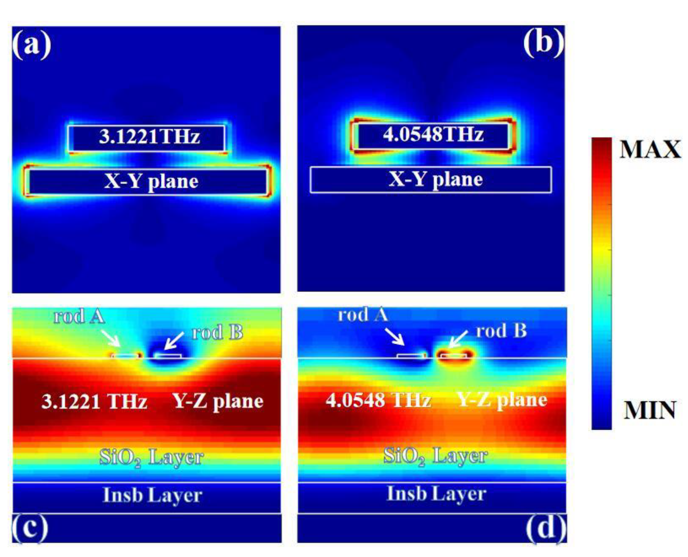
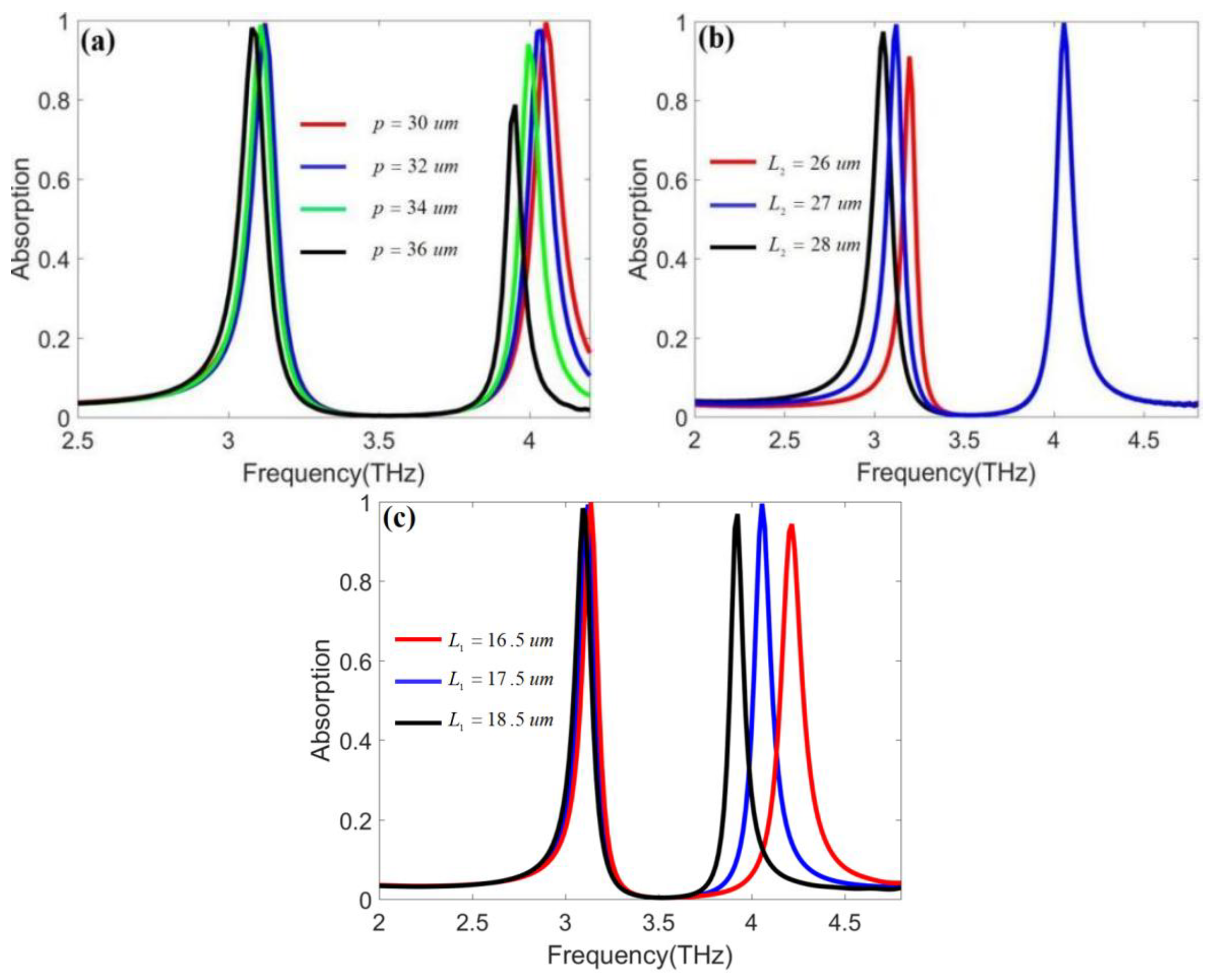
3. Results and Discussion

Figure 4 presents the absorption, reflection, and transmission curves of the dual-band absorber model. The BDS Fermi energy is E F = 0.13   eV , and the InSb temperature is T = 475   K . At first, the applied magnetic field is B = 0   T .
In Figure 4a, the absorber achieves high absorption rates of 99.3% and 99.6% at frequencies of 3.1221 THz and 4.0548 THz, respectively, with an average absorption rate of 99.4%. Meanwhile, as shown in Figure 1c, InSb exhibits metallic characteristics when the temperature is T = 475   K , and its thickness is greater than the skin depth of the incident light in the THz range. As a result, within the analyzed frequency range, the transmittance of the dual-band model remains zero.
On the other hand, as shown in Figure 4b, both rods A and B exhibit the Lorentzian resonances, demonstrating that they can be considered as bright mode units that engage in the direct interaction with incident light. Moreover, it can be observed that the absorption frequencies of rod A (blue dashed line) and rod B (red dashed line) are nearly equivalent to the absorption frequencies at peak A and peak B, respectively. Hence, the dual-band absorption effect can be interpreted as the consequence of the bright–bright coupling between rods A and B [38,39,40].
Finally, according to the results of ECM in Figure 4c, the real parts of the equivalent impedance Z r of the dual-band model at peaks A and B are equal to 1, while the imaginary parts are near to 0, achieving impedance matching. Therefore, the model exhibits the perfect absorption effect at peaks A and B.
Figure 5 presents the electric field intensity distributions of the dual-band absorber model at peaks A and B in the X-Y and Y-Z planes, respectively.
As illustrated in Figure 4b, the rods A and B can be considered as bright-mode units, and the absorption frequencies of rod A and rod B are nearly equivalent to the absorption frequencies at peak A and peak B. Hence, as shown in Figure 5a,b, the electric field in the X-Y plane exhibits dipole mode distribution, and mainly concentrates on the both sides of rods A and B, respectively [41]. Additionally, as shown in Figure 5c,d, the electric field in the Y-Z plane is primarily concentrated on the rod A, rod B, and SiO2 layers. Moreover, the electric field intensity in InSb layer is almost equal to zero because the InSb is in metallic state.
Figure 6 illustrates the variations in the absorption spectra under different parameters of dual-band absorber.
In Figure 6a, as the model period p increases, the absorption frequencies at peaks A and B decrease, resulting in red-shift. Additionally, the absorption rates at peak B decrease continuously, while the absorption rates at peak A remain relatively constant. In Figure 6b, the absorption frequencies at peak A decrease and exhibit red-shift as the L 2 increases, due to the relationship between absorption frequency and the length of nanorod, which can be represented by f 1 / L . Moreover, the absorption frequencies and rates at peak B are almost unchanged. Similarly, when the L 1 increases, the absorption frequencies at peak B also decrease, red-shift occurs, and the absorption frequencies and rates at peak A remain almost constant, as shown in Figure 6c.
In Figure 7a, the thickness of the SiO2 layer plays a crucial role in controlling the interaction between the BDS rod and incident light, because the BDS rod, SiO2 layer, and InSb layer construct an equivalent F-P resonator. Therefore, as the thickness increases, the absorption frequencies at peaks A and B decrease, resulting in red-shift. Additionally, as the h 2 varies from h 2 = 20   μ m to h 2 = 26   μ m , the absorption rates at peak A first decrease and then increase, while the absorption rates at peak B continue to decrease. When the SiO2 layer thickness is h 2 = 20   μ m , the absorption rates at peak A and peak B reach their maximum values.
In Figure 7b, when the thickness of InSb is h 3 5   μ m , the absorption rates of the dual-band absorber remain constant because the thickness of InSb is greater than the skin depth of incident light, and the transmission channel of the model has been closed. The system exhibits two prominent absorption peaks. Moreover, as the thickness of InSb decreases, the absorption rates and frequencies at peaks A and B also decrease gradually. Finally, when the thickness of InSb is h 3 0.2   μ m , the absorption rates and frequencies of the system reach the minimum values and remain constant.

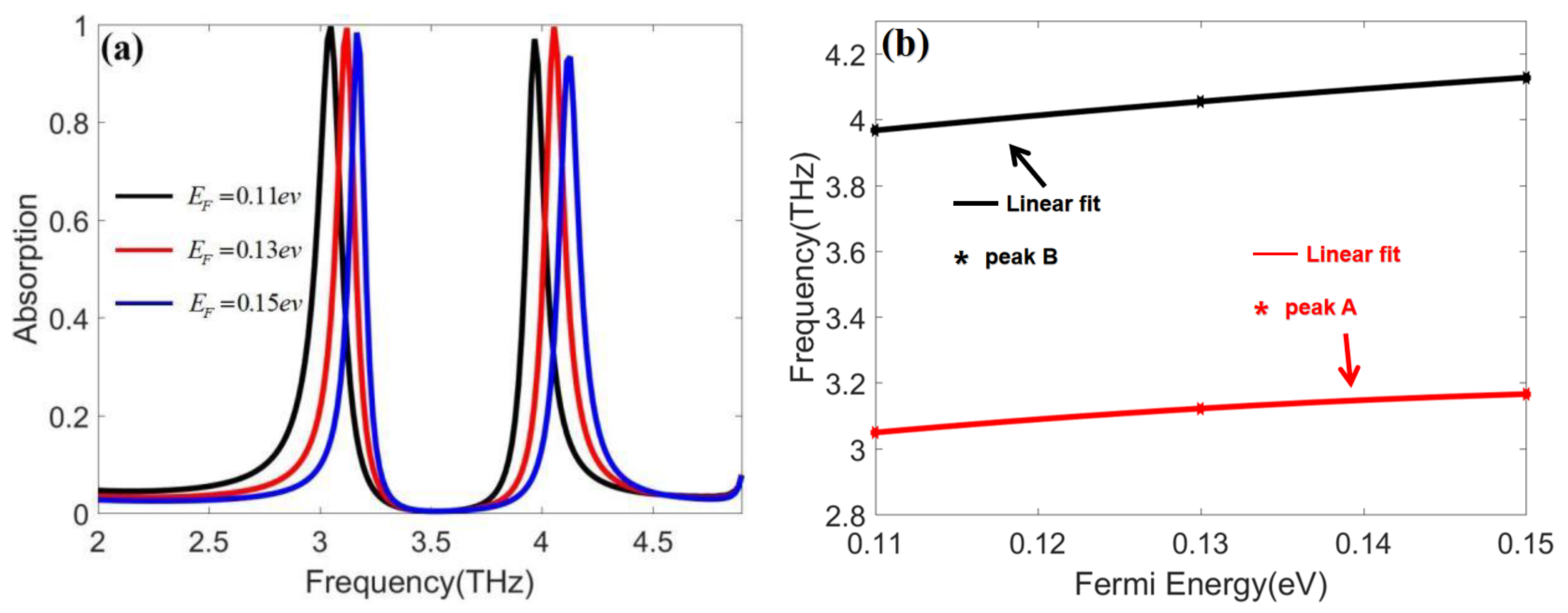
4. Electrically Tunable Characteristics of Dual-Band Absorber

The variations in the dual-band absorber model with different BDS Fermi energies are depicted in Figure 8. The temperature of InSb is T = 475   K , and the magnetic field is B = 0   T .
As illustrated in Figure 1a, when the Fermi energies of BDS increase, the real parts of the dielectric constants of BDS decrease. Meanwhile, according to perturbation theory [42], the absorber’s resonant frequencies will increase if the real components of the dielectric constant decrease. Thus, as illustrated in Figure 8a, when the BDS Fermi energies increase, the absorber’s absorption frequencies at peaks A and B gradually rise, resulting in blue-shift. Furthermore, the absorption rates at peak A are almost unchanged, and the absorption rates at peak B first increase and then decrease.
In Figure 8b, when the BDS Fermi energies increase, the variations in absorption peaks A and B also show an approximately linear relationship with the changes in the Fermi energies. When the Fermi energy increases from 0.11 eV to 0.13 eV, the absorption frequencies of peak A increase from 3.05 THz to 3.17 THz, and the absorption frequencies at peak B increase from 3.97 THz to 4.13 THz
Therefore, the dual-band absorber model can achieve electrically tunable characteristics by varying the BDS Fermi energy.

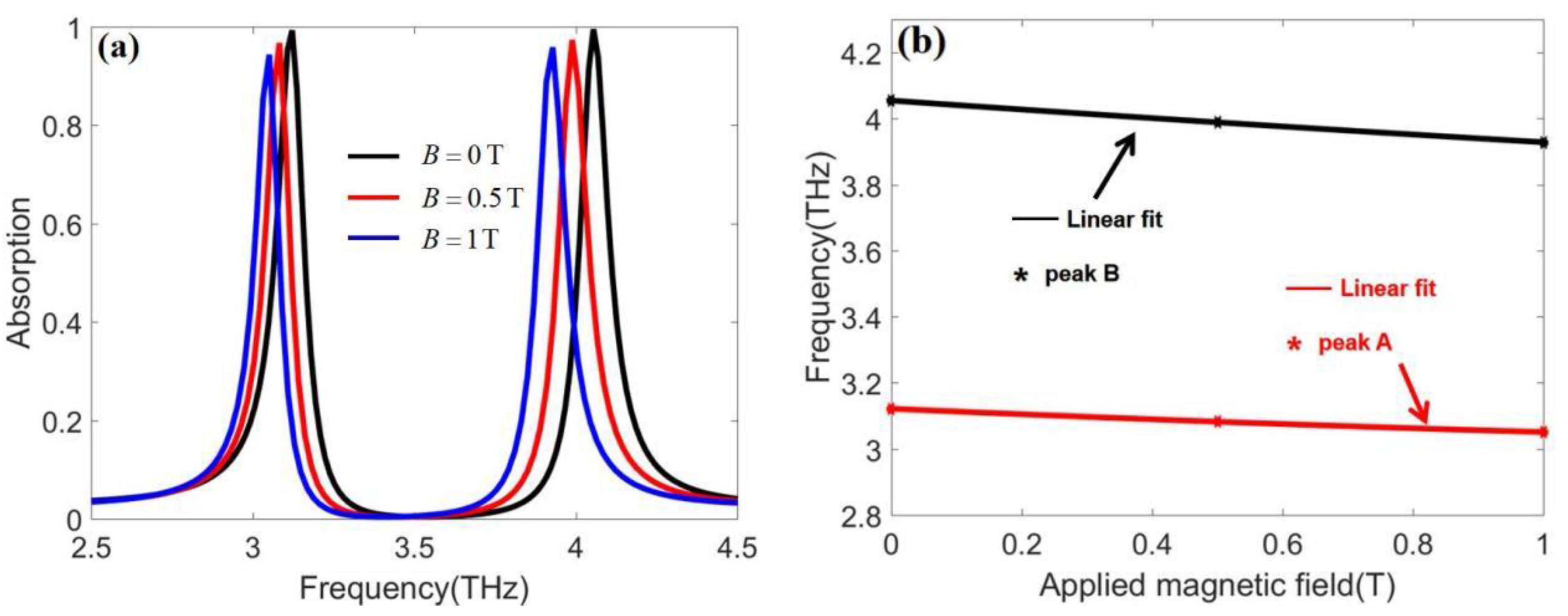
5. Thermally and Magnetically Tunable Characteristics of Dual-Band Absorber

The variations in the dual-band absorber model with different InSb temperatures are depicted in Figure 9. The BDS Fermi energy is E F = 0.13   eV , and the applied magnetic field is B = 0   T .
As shown in Figure 9a, the absorption rates at peaks A and B continuously increase as the temperatures increase. When the temperature is T = 475   K , the absorption rates at peaks A and B are 99.3% and 99.6%, respectively.
Furthermore, in Figure 9b, when the temperatures of InSb increase from T = 325   K to T = 475   K , the absorption frequencies at peak A increase from 2.87 THz to 3.12 THz, and the absorption frequencies at peak B also increase from 3.54 THz to 4.05 THz, because the real parts of the dielectric constants of InSb will decrease when the temperature increases, as shown in Figure 1c.
Especially, it can be found that when the temperature changes from T = 325   K to T = 375   K (50 °C < 100 °C), the absorption frequencies of peak B increase from 3.54 THz to 3.97 THz. Hence, the temperature sensitivity at peak B can be calculated as S = Δ f / Δ T = 0.0085 THz/°C.
The variations in the dual-band absorber model with different applied magnetic field B are depicted in Figure 10. The applied magnetic field is along X axis direction. The BDS Fermi energy is E F = 0.13   eV , and the InSb temperature is T = 475   K .
As discussed above, the state of InSb will be altered from isotropic to anisotropic, and the permittivity tensor of InSb can be adjusted with the variation in the applied magnetic field B. Hence, as shown in Figure 10a, when the applied magnetic field B is varied from B = 0   T to B = 1   T , the absorption frequencies and rates at peaks A and B decrease gradually [30]. Moreover, the variations in absorption frequencies at two absorption peaks also show an approximately linear relationship with the changes in the applied magnetic fields in Figure 10b.
Therefore, the dual-band absorber model can achieve thermally and magnetically tunable characteristics by varying the InSb temperature and applied magnetic field.
Finally, Figure 11 analyzes the application prospects of the dual-band absorber as a refractive index sensor. In Figure 11a, as the background refractive index increases, noticeable red-shift occurs in the absorption frequencies at peaks A and B. Additionally, in Figure 11b, when the refractive index changes, the variations in peaks A and B also show an approximately linear relationship with the changes in the refractive index.
By calculating the sensitivity S = Δ λ / Δ n and the figure of merit F O M = S / F W H M , we obtain that the sensitivity of peak A is S = 20.88   μ m / RIU and figure of merit is F O M = 6.06   RIU 1 . Similarly, at peak B, the sensitivity is S = 15.25   μ m / RIU and figure of merit is F O M = 7.05   RIU 1 . The sensitivity and FOM are higher than the similar index sensors shown in papers [43,44], and the absorber proposed also exhibits excellent sensing performances.

6. Conclusions

In this paper, the electrically, thermally, and magnetically tunable dual-band metamaterial absorber based on BDS and InSb is proposed. The average absorption rate of the dual-band absorber is 99.4%, and the perfect absorption effect is achieved. Additionally, the ECM and electrical field intensity distributions at absorption peaks are employed to conduct a theoretical analysis of the absorbers’ behaviors. By varying the BDS Fermi energy, InSb temperature, and applied magnetic field, the dynamic triple-tuning of absorption frequencies and rates of absorber can be realized. Finally, the influences of model parameters on the absorption performances of the dual-band absorber and its potential applications as a refractive index and temperature sensors are further discussed.

Author Contributions

Conceptualization and model, B.H.; numerical simulation, B.H. and L.Y.; writing—original draft preparation, B.H. and M.H.; investigation and formal analysis C.C.; writing—review and editing, B.H., M.H. and L.Y.; project administration and resources, B.H. and M.H. All authors have read and agreed to the published version of the manuscript.

Funding

This work is partially funded by National Natural Science Foundation of China (NSFC) (Grant Nos. 61461052, 11564044, and 61863035). Yunnan Provincial Department of Science and Technology Agricultural Joint Special Project (Grant Nos. 202101BD070001-064) and Yunnan Province Basic Research Project (Grant Nos. 202301AT070495).

Institutional Review Board Statement

Not applicable.

Informed Consent Statement

Not applicable.

Data Availability Statement

The data supporting the findings of this study are available within the article.

Conflicts of Interest

The authors declare no conflicts of interest.

References

  1. Withayachumnankul, W.; Abbott, D. Metamaterials in the terahertz regime. IEEE Photonics J. 2009, 1, 99. [Google Scholar] [CrossRef]
  2. Chen, H.-T.; Padilla, W.J.; Cich, M.J.; Azad, A.K.; Averitt, R.D.; Taylor, A.J. A metamaterial solid-state terahertz phase modulator. Nat. Photonics 2009, 3, 148. [Google Scholar] [CrossRef]
  3. Fan, K.; Zhao, X.; Zhang, J. Optically tunable terahertz metamaterials on highly flexible substrates. IEEE Trans. Terahertz Sci. Technol. 2013, 3, 702. [Google Scholar] [CrossRef]
  4. Kojima, S.; Mori, T. Terahertz time-domain spectroscopy of Raman inactive phonon-polariton in strontium titanate. Ferroelectrics 2016, 499, 100. [Google Scholar] [CrossRef]
  5. Xu, W.; Xie, L.; Ying, Y. Mechanisms and applications of terahertz metamaterial sensing: A review. Nanoscale 2017, 9, 13864. [Google Scholar] [CrossRef]
  6. Sheta, E.M.; Choudhury, P.K. Graphene-strontium titanate-based metamaterial for optical sensing. Proc. SPIE 2021, 11802, 147. [Google Scholar]
  7. Diem, M.; Koschny, T.; Soukoulis, C.M. Wide-angle perfect absorber/thermal emitter in the terahertz regime. Phys. Rev. B 2009, 79, 033101. [Google Scholar] [CrossRef]
  8. Cheng, D.; He, X.; Huang, X.; Zhang, B.; Liu, G.; Shu, G.; Fang, C.; Wang, J.; Luo, Y. Terahertz biosensing metamaterial absorber for virus detection based on spoof surface plasmon polaritons. Int. J. RF Microw. Comput. Aided Eng. 2018, 28, e21448. [Google Scholar] [CrossRef]
  9. Sekhi, S.Z.; Shokooh-Saremi, M.; Mirsalehi, M.M. Ultra-broadband wide-angle and polarization-insensitive metamaterial perfect absorber for solar energy harvesting. J. Nanophotonics 2020, 14, 046014. [Google Scholar] [CrossRef]
  10. Wang, H.; Sivan, V.P.; Mitchell, A. Highly efficient selective metamaterial absorber for high-temperature solar thermal energy harvesting. Sol. Energy Mater. Sol. Cells 2015, 137, 235. [Google Scholar] [CrossRef]
  11. Zhang, Y.; Lv, J.; Que, L. A double-band tunable perfect terahertz metamaterial absorber based on Dirac semimetals. Results Phys. 2019, 15, 102773. [Google Scholar] [CrossRef]
  12. Meng, W.; Que, L.; Lv, J. A triple-band terahertz metamaterial absorber based on buck Dirac semimetals. Results Phys. 2019, 14, 102461. [Google Scholar] [CrossRef]
  13. Liu, G.D.; Zhai, X.; Meng, H.Y. Dirac semimetals based tunable narrowband absorber at terahertz frequencies. Opt. Express 2018, 26, 11471–11480. [Google Scholar] [CrossRef] [PubMed]
  14. Fang, P.; Shi, X.; Liu, C. Single-and dual-band convertible terahertz absorber based on bulk Dirac semimetal. Opt. Commun. 2020, 462, 125333. [Google Scholar] [CrossRef]
  15. Liu, Z.; Zhang, Z.; Zhou, F. Dynamically tunable electro-optic switch and multimode filter based on twisted bilayer graphene strips. J. Opt. 2021, 23, 025104. [Google Scholar] [CrossRef]
  16. Cheng, H.; Chen, S.; Yu, P. Dynamically tunable plasmonically induced transparency in periodically patterned graphene nanostrips. Appl. Phys. Lett. 2013, 103, 203112. [Google Scholar] [CrossRef]
  17. Zhou, F.; Wang, Y.; Zhang, X. Dynamically adjustable plasmon-induced transparency and switching application based on bilayer graphene metamaterials. J. Phys. D Appl. Phys. 2020, 54, 054002. [Google Scholar] [CrossRef]
  18. Lherbier, A.; Biel, B.; Niquet, Y.M. Transport length scales in disordered graphene-based materials: Strong localization regimes and dimensionality effects. Phys. Rev. Lett. 2008, 100, 036803. [Google Scholar] [CrossRef]
  19. Liang, J.R.; Wu, M.J.; Hu, M. Fabrication of VO2 thin film by rapid thermal annealing in oxygen atmosphere and its metal—Insulator phase transition properties. Chin. Phys. B 2014, 23, 076801. [Google Scholar] [CrossRef]
  20. Liu, Y.N.; Weng, X.L.; Zhang, P. Ultra-broadband infrared metamaterial absorber for passive radiative cooling. Chin. Phys. Lett. 2021, 38, 034201. [Google Scholar] [CrossRef]
  21. Nouman, M.T.; Hwang, J.H.; Faiyaz, M. Vanadium dioxide based frequency tunable metasurface filters for realizing reconfigurable terahertz optical phase and polarization control. Opt. Express 2018, 26, 12922. [Google Scholar] [CrossRef] [PubMed]
  22. Wahlstrand, J.K.; Heilweil, E.J. Contactless THz-based bulk semiconductor mobility measurements using two-photon excitation. Opt. Express 2018, 26, 29848. [Google Scholar] [CrossRef] [PubMed]
  23. Kowerdziej, R.; Jaroszewicz, L. Tunable dual-band liquid crystal based near-infrared perfect metamaterial absorber with high-loss metal. Liq. Cryst. 2019, 46, 1568. [Google Scholar] [CrossRef]
  24. Baranzadeh, F.; Nozhat, N. High Performance Plasmonic Nano-Biosensor Based on Tunable Ultra-Narrowband Perfect Absorber Utilizing Liquid Crystal. Plasmonics 2021, 16, 253. [Google Scholar] [CrossRef]
  25. Mistry, D.; Traugutt, N.A.; Sanborn, B. Soft elasticity optimises dissipation in 3D-printed liquid crystal elastomers. Nature 2021, 12, 6677. [Google Scholar] [CrossRef] [PubMed]
  26. Kumar, P.; Lakhtakia, A.; Jain, P.K. Tricontrollable pixelated metasurface for absorbing terahertz radiation. Appl. Opt. 2019, 58, 9614. [Google Scholar] [CrossRef] [PubMed]
  27. Liang, Y.; Pakniyat, S.; Xiang, Y. Temperature-dependent transverse-field magneto-plasmons properties in InSb. Opt. Mater. 2021, 112, 110831. [Google Scholar] [CrossRef]
  28. Li, H.; Huang, W.; Zhang, W. Thermally controlled electromagnetically induced transparency in hybrid metal-InSb metamaterials at THz frequencies. J. Phys. Conf. Ser. 2020, 1592, 012024. [Google Scholar] [CrossRef]
  29. Kang, W.; Gao, Q.; Dai, L. Dual-controlled tunable terahertz coherent perfect absorption using Dirac semimetal and vanadium dioxide. Results Phys. 2020, 19, 103866. [Google Scholar] [CrossRef]
  30. Jing, H.; Wei, Y.; Duan, J. Thermally and magnetically controlled dual-band terahertz metamaterial absorber based on InSb. Opt. Mater. 2022, 129, 112311. [Google Scholar] [CrossRef]
  31. Hu, B.J.; Huang, M.; Yang, L. Terahertz dual-tunable absorber based on hybrid gold-graphene-strontium titanate-vanadium dioxide configuration. Opt. Mater. Express 2023, 13, 2775. [Google Scholar] [CrossRef]
  32. Kotov, O.V.; Lozovik, Y.E. Dielectric response and novel electromagnetic modes in three-dimensional Dirac semimetal films. Phys. Rev. B 2016, 93, 235417. [Google Scholar] [CrossRef]
  33. Zhou, J.; Chang, H.R.; Xiao, D. Plasmon mode as a detection of the chiral anomaly in Weyl semimetals. Phys. Rev. B 2015, 91, 035114. [Google Scholar] [CrossRef]
  34. Lv, M.; Zhang, S.C. Dielectric function, Friedel oscillation and plasmons in Weyl semimetals. Int. J. Mod. Phys. B 2013, 27, 1350177. [Google Scholar] [CrossRef]
  35. Ziaee, B.M.; Forooraghi, K.; Atlasbaf, Z. Method of lines for analysis of plane wave scattering by periodic arrays of magnetically-biased graphene strips. Sci. Rep. 2021, 11, 7588. [Google Scholar]
  36. Han, J.; Lakhtakia, A.; Qiu, C.W. Terahertz metamaterials with semiconductor split-ring resonators for magnetostatic tunability. Opt. Express 2008, 16, 14390. [Google Scholar] [CrossRef]
  37. Huang, J.; Li, J.; Yang, Y. Active controllable dual broadband terahertz absorber based on hybrid metamaterials with vanadium dioxide. Opt. Express 2020, 28, 7018. [Google Scholar] [CrossRef] [PubMed]
  38. Hu, B.J.; Huang, M.; Li, P. Dynamically dual-tunable dual-band to four-band metamaterial absorbers based on bulk Dirac semimetal and vanadium dioxide. J. Opt. Soc. Am. A 2022, 39, 383. [Google Scholar] [CrossRef] [PubMed]
  39. Chen, M.M.; Yang, X.X. Polarization-insensitive electromagnetically induced transparency and its sensing performance based on spoof localized surface plasmons in vanadium dioxide-based terahertz metasurfaces. Phys. Chem. Chem. Phys. 2023, 25, 21047. [Google Scholar] [CrossRef]
  40. Ge, Z.K.; Sang, T.; Luo, C. Configurable dual-topological-interface-states induced reflection in hybrid multilayers consisting of a Ge2Sb2Te5 film. Opt. Express 2024, 32, 16351. [Google Scholar] [CrossRef]
  41. Liu, Y.; Zhong, R.; Lian, Z. Dynamically tunable band stop filter enabled by the metal-graphene metamaterials. Sci. Rep. 2018, 8, 2828. [Google Scholar] [CrossRef] [PubMed]
  42. Hwang, J.; Roh, J.W. Electrically tunable two-dimensional metasurfaces at near-infrared wavelengths. Opt. Express 2017, 25, 25071. [Google Scholar] [CrossRef] [PubMed]
  43. Jia, W.; Ren, P.; Jia, Y. Active control and large group delay in graphene-based terahertz metamaterials. J. Phys. Chem. C 2019, 123, 18560. [Google Scholar] [CrossRef]
  44. Xiao, B.; Tong, S.; Fyfe, A. Tunable electromagnetically induced transparency based on graphene metamaterials. Opt. Express 2020, 28, 4048. [Google Scholar] [CrossRef] [PubMed]
Figure 1. Variations in the dielectric constant of BDS: (a) real parts and (b) imaginary parts with different Fermi energies. Variations in the dielectric constant of InSb: (c) real parts and (d) imaginary parts with different temperatures.
Photonics 11 01039 g001
Figure 2. Schematic diagrams of the dual-band absorber: (a) 3D view, (b) top view, (c) side view.
Photonics 11 01039 g002
Figure 3. Equivalent circuit model of proposed dual-band absorber.
Photonics 11 01039 g003
Figure 4. (a) Absorption, reflection, and transmission curves of the dual-band absorber; (b) relationships between the absorption curves of rods A and B and the dual-band model; (c) ECM analysis results of the dual-band absorber model.
Photonics 11 01039 g004aPhotonics 11 01039 g004b
Figure 5. Electric field distributions of the dual-band absorber model in the X-Y and Y-Z planes. (a) 3.1221 THz in X-Y plane, (b) 4.0548 THz in X-Y plane, (c) 3.1221 THz in Y-Z plane, (d) 4.0548 THz in Y-Z plane.
Photonics 11 01039 g005
Figure 6. The variation trends in absorber model with respect to (a) period, (b) length of rod A, and (c) length of rod B.
Photonics 11 01039 g006
Figure 7. Variation trends in the absorber model with respect to (a) SiO2 layer thickness and (b) InSb layer thickness.
Photonics 11 01039 g007
Figure 8. Variation trends in (a) absorption spectra and (b) absorption frequencies with different BDS Fermi energies.
Photonics 11 01039 g008
Figure 9. Variation trends in (a) absorption spectra and (b) absorption frequencies with different InSb temperatures.
Photonics 11 01039 g009
Figure 10. Variation trends in (a) absorption spectra and (b) absorption frequencies with different applied magnetic fields.
Photonics 11 01039 g010
Figure 11. (a) Variation trends in absorption spectra, (b) Variation trends in peak A and peak B with different background refractive indices.
Photonics 11 01039 g011
Disclaimer/Publisher’s Note: The statements, opinions and data contained in all publications are solely those of the individual author(s) and contributor(s) and not of MDPI and/or the editor(s). MDPI and/or the editor(s) disclaim responsibility for any injury to people or property resulting from any ideas, methods, instructions or products referred to in the content.

