Abstract
A bidirectional resonant converter is presented and verified in this paper for an electric vehicle battery charger/discharger system. The presented circuit can achieve forward and backward power operation, low switching losses on active devices, and wide output voltage operation. The circuit structure of the presented converter includes two resonant circuits on the primary and secondary sides of an isolated transformer. The frequency modulation approach is adopted to control the studied circuit. Owing to the resonant circuit characteristic, active devices for both forward (battery charge) and backward (battery discharge) power operation can be turned on at zero voltage switching. In order to implement a universal battery charger for different kinds of electric vehicle applications, the DC converter is demanded to have a wide output voltage range capability. The topology morphing between a full bridge resonant circuit and half bridge resonant circuit is selected to obtain high- and low-output voltage range operations so that the 200–500 V output voltage range is realized in the presented resonant converter. Compared to the conventional bidirectional converters, the proposed can be operated under a wide voltage range operation. In the end, a 1 kW laboratory prototype circuit is built, and experiments are provided to demonstrate the validity and performance of the presented bidirectional resonant converter.
1. Introduction
For the development of renewable energy, the DC microgrid or nanogrid systems have been widely studied to support one of local power distribution networks. The DC/DC converters or AC/DC converters [1,2,3,4,5] are demanded to convert unstable DC voltage from solar power or fuel cell power or unstable AC voltage from wind power into a stable DC bus voltage. Then, the DC bus voltage on the DC microgrid can supply power to residential houses, commercial buildings, and industry factories. Normally, DC/DC converters or DC/AC converters are needed to convert the DC bus voltage into low DC voltage for commercial or personal power units or AC voltage for motor drives. In order to reduce oil demand and air pollution, electric vehicles have been widely developed in recent years with using battery packs instead of gasoline as their power source. Therefore, the bidirectional AC/DC or DC/DC converters are demanded [6,7,8] to achieve battery charge and discharge. In [9,10], the phase-shift pulse-width modulation (PWM) converter has been proposed to achieve buck/boost operation under forward/backward power flow operation. However, this circuit topology has high circulating current loss at freewheeling state and low circuit efficiency at low duty cycle operation if the wide voltage range is demanded. In [11,12,13,14], dual active bridge (DAB) PWM converters have been developed and implemented to have bidirectional power operation with Vo = 300–450 V voltage range. The phase shift technique and duty cycle control are used in DAB converters to control power flow between input and output terminals. However, the phase angle between two terminals and duty cycle PWM signals are more complicated to calculate and derived compared to these other bidirectional power converters. In [15,16], the symmetric resonant converters have been studied and achieved to realize bidirectional power operation using the frequency modulation approach. Therefore, the active devices can be turned on at zero voltage switching. However, the input or output voltage of this circuit topology is limited at a finite range such as 400–600 V input or 300–450 V output voltage range. The advantage of the resonant converter is the low switching loss on active devices and has been discussed in [15,16]. However, the symmetric resonant converter cannot achieve well if the wide voltage range operation is demanded for universal battery charge/discharge circuit.
A bidirectional DC/DC converter is presented to have low switching loss on active devices, forward/backward power operation, and wide voltage operation for battery charge/discharge applications on a DC microgrid system. The input voltage of the presented converter is from DC bus voltage on DC microgrid system. For forward power operation, power flow is from DC microgrid to battery. For backward power operation, power flows is from battery to DC microgrid. Two full bridge resonant circuits are used in the studied converter to achieve bidirectional power flow capability. The power flow and voltage regulation are controlled by using a frequency modulation approach. The adopted resonant circuit has a soft switching characteristic for all power switches. Thus, the switching loss on active devices is reduced. The variable half/full bridge resonant circuit structure is used in the presented converter to solve limit voltage gain disadvantage on conventional bidirectional resonant converters. When low voltage output is requested, the half bridge resonant circuit is operated to achieve low voltage gain. If the high output is demanded in the proposed converter, full bridge resonant circuit is operated to realize high voltage gain. Thus, a wide output voltage operation is implemented in the studied circuit. The presented bidirectional DC/DC converter can be applied to a universal battery charge/discharge system in electric vehicle systems or battery charge stations. The circuit schematic is presented in Section 2. The operation of principle is discussed in Section 3. The circuit analysis and design example are provided in Section 4. Experiments are provided in Section 5 to verify the performance of the proposed converter. In Section 6, a conclusion of the studied DC converter is provided.
2. Circuit Schematic of the Presented Converter
Figure 1 shows the block diagrams of the simplified DC nanogrid or microgrid system. Normally, the DC microgrid inputs can be DC power (solar power, fuel cell power, or HVDC transmission supply) or AC power (AC transmission supply or wind power). The microgrid outputs may be AC loads (motor drives), DC loads (personal computers or server systems), or battery stacks in electric vehicle applications. For residential house or industry factory applications, the bus voltage of DC microgrid system is normally controlled at 380 V. For modern battery charger/discharger system in electric vehicle applications, the bidirectional DC/DC converter is demanded to achieve grid-to-vehicle (G2V) and vehicle-to-grid (V2G) power flow operations. The conventional buck/boost converter shown in Figure 2a is used to realize forward and backward power flows for battery charge and discharge operations. However, no electric isolation is given in bidirectional buck/boost converter. Figure 2b gives the circuit diagram of a dual active bridge converter to achieve bidirectional power operation. By controlling the phase-angle between the leg voltages Vab and Vcd, the forward or backward power can be regulated and controlled between input and output terminals. However, dual active bridge converter has the circulating current losses at the freewheeling state. Figure 2c gives the circuit diagram of a dual resonant converter to realize bidirectional power flow operations. The symmetric resonant circuits are adopted on the primary and secondary sides so that the converter operated at forward power and backward power operations has similar circuit characteristics. The advantages of the resonant converters [17,18] are low switching losses on power devices and low electromagnetic interference. However, the dual resonant converter has less voltage gain so that the available input or output voltage is limited at a finite range.
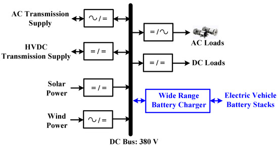
Figure 1.
Block diagram of a simplified DC microgrid system.
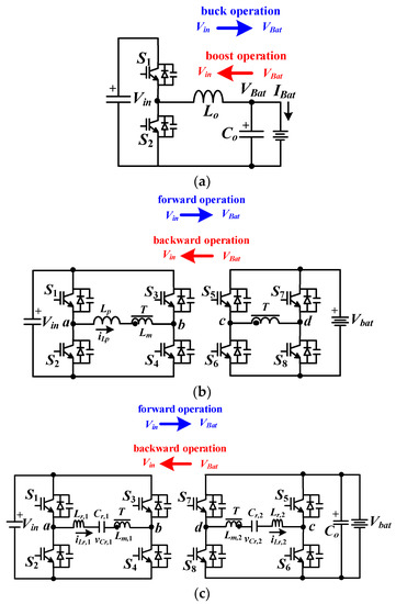
Figure 2.
Circuit diagrams of bidirectional DC/DC converter: (a) buck/boost converter; (b) dual active bridge converter; (c) dual resonant converter.
The circuit schematic of the presented converter is shown in Figure 3a. Compared to the conventional dual resonant converter, the proposed converter has more wide output voltage range operation with bidirectional power flow operation and soft switching operation on all active devices. Full bridge circuit and one additional ac switch Sac are adopted on the input voltage terminal. Similarly, the other full bridge circuit is adopted on the output voltage terminal in the proposed circuit. For forward power operation, S5–S8 are off so that the secondary side circuit is similar to a full bridge diode rectifier. When low-output voltage range is demanded to charge the battery stack, Sac is on and S3 and S4 are off. Only S1 and S2 are controlled by the frequency modulation scheme. Figure 3b gives the equivalent circuit structure of the presented converter operated at low-output voltage range and forward power operation. One can observe that the equivalent circuit in Figure 3b is a half bridge resonant circuit. When high-output voltage range is requested to charge battery stack, Sac is off and S1–S4 are controlled with frequency modulation scheme. The equivalent circuit of the presented converter operated at forward power operation and high-output voltage range is shown in Figure 3c. Basically, the circuit in Figure 3c is a full bridge resonant converter. Since the leg voltage Vab in Figure 3c (full bridge resonant circuit) is two times that of the leg voltage Vac in Figure 3b (half bridge resonant circuit), the presented converter has a larger output voltage under full bridge resonant structure (Figure 3c) than half bridge resonant structure (Figure 3b). For backward power operation, the switches S5–S8 are controlled with variable frequency modulation to transfer power from Vo side to Vin. Since the Vo is discharged from a high-voltage level, full bridge diode rectifier is adopted on the left hand side of the proposed circuit. Therefore, S5–S8 and Sac are all off and the equivalent circuit under backward power operation is shown in Figure 3d.
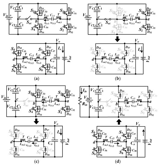
Figure 3.
Proposed resonant converter with bidirectional power flow and wide output voltage operation: (a) circuit structure; (b) forward power flow and low output voltage range; (c) forward power flow and high-output voltage range; (d) backward power operation.
3. Principle of Operation
The presented circuit has three different operation modes as shown in Figure 3b–d to achieve bidirectional power operation and wide output voltage operation. Three operation modes are presented in the following discussions. Figure 4 gives the voltage and current waveforms for these three operation modes. For every switching cycle, there are eight operating states according to the conducting status of switches and diodes.
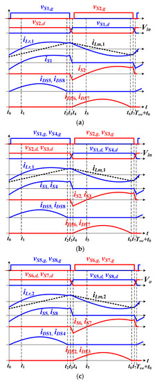
Figure 4.
Main voltage and current waveforms of the proposed converter at (a) forward power operation and low-output voltage range; (b) forward power operation and high-output voltage range; (c) backward power operation.
3.1. Low-Output Voltage Range under Forward Power Operation
If the battery stack is at a low-voltage level, the proposed converter is needed to output low voltage. In order to achieve wide output voltage range operation, the half bridge resonant circuit as shown in Figure 3b is adopted to accomplish forward power operation. Switch Sac is on and S3, S4 and S5–S8 are off. Only S1 and S2 are controlled with frequency modulation approach. The secondary side is similar to a full bridge diode rectifier. According to the status of active switches and diodes, eight switching states are observed in every switching cycle as shown in Figure 4a if fsw < fr (resonant frequency). To simplify the circuit discussion, the circuit components are assumed as Cr,1 = Cr,2/n2 and Lr,1 = n2Lr,2 where n = np/ns so that the converter has same resonant frequency for both forward and backward power operations. Figure 5 gives the circuits of these eight switching states.
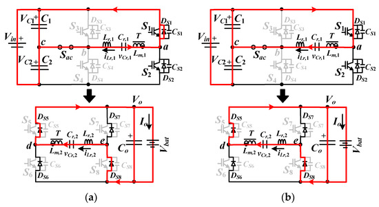
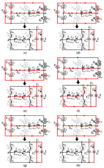
Figure 5.
Equivalent circuits under low-output voltage range and forward power operation: (a) state 1; (b) state 2; (c) state 3; (d) state 4; (e) state 5; (f) state 6; (g) state 7; (h) state 8.
- State 1 [t0, t1]: vCS1 = 0 at t0. Since iLr,1(t0) < 0, the anti-parallel diode DS1 conducts. Therefore, switch S1 turns on at this moment to achieve zero voltage switching. The current iLr,2 increases and DS5 and DS8 are forward biased.
- State 2 [t1, t2]: At t1, iLr,1 > 0 so that diode DS1 becomes off and iLr,1 flows through S1 instead of DS1. Power is transferred from VC1 to Vo in this state. The input and output leg voltages are Vac = VC1 = Vin/2 and Vde = Vo. In this state, the resonant frequency is .
- State 3 [t2, t3]: If fsw < fr, iLr,2 = 0 at t2. Thus, DS5 and DS8 are off. Since C1 >> Cr,1, the resonant frequency in state 3 is given as .
- State 4 [t3, t4]: S1 turns off at t3. Then, iLr,1 will charge CS1 and discharge CS2. If the current where CS,1 = CS1 = CS2 = CS3 = CS4 and iLm,1,peak is the peak value of iLm,1, then CS2 can be discharged to zero voltage.
- State 5 [t4, t5]: vCS2 = 0 at t4. Since iLr,1(t4) > 0, the anti-parallel diode DS2 conducts. Therefore, S2 can be turned on at this moment to realize zero voltage switching. The current iLr,2 decreases so that DS6 and DS7 are conducting.
- State 6 [t5, t6]: At t5, iLr,1 < 0 so that DS2 is off. iLr,1 flows through S2. Power is transferred from VC2 to Vo in state 6. The resonant frequency in state 6 is .
- State 7 [t6, t7]: At time t6, iLr,2 = 0. Then, DS6 and DS7 become off. Since C2 >> Cr,1, the resonant frequency in state 7 is .
- State 8 [t7, Tsw + t0]: At time t7, S2 is turned off. Since iLr,1(t7) < 0, CS1 (CS2) is discharged (charged) in this state. This switching cycle is ended at time Tsw + t0.
3.2. High-Output Voltage Range under Forward Power Operation
When high-output voltage range is demanded in the proposed converter, the full bridge resonant converter is selected on the primary side to achieve high voltage gain. Therefore, Sac is off and S1–S4 are controlled with frequency modulation to regulate the load voltage. Switches S5–S8 are off and the secondary side operates as a full bridge diode rectifier. Owing to the status of S1–S4 and DS5–DS8, eight switching states are operated in every switching cycle as shown in Figure 4b. The circuits of these eight switching states are provided in Figure 6. Since the full bridge resonant circuit in Figure 6 and half bridge resonant circuit in Figure 5 have the similar operation states with differnent voltage gains, the state operations of the presented converter operated at high-output voltage range under forward power operation are neglected in this subsection.
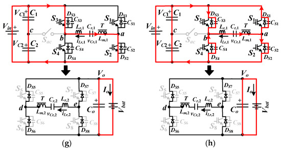
Figure 6.
Equivalent circuits under high-output voltage range and forward power operation: (a) state 1; (b) state 2; (c) state 3; (d) state 4; (e) state 5; (f) state 6; (g) state 7; (h) state 8.
3.3. Under Backward Power Operation
When the presented converter is demanded to achieve backward power operation, the circuit operation under reverse power transfer from Vo to Vin is given in Figure 3d. Switch Sac and S1–S4 are off and S5–S8 are controlled with frequency modulation. The full bridge diode rectifier and full bridge resonant circuit are operated on the left and right hand sides, respectively, of the presented circuit. Based on status of S5–S8 and DS1–DS4, the proposed converter operated in Figure 3d has eight switching states (Figure 4c) in every switching cycle. Figure 7 provides eight state circuits under backward power operation.
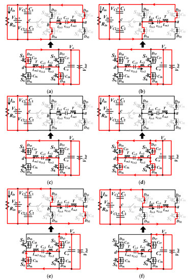
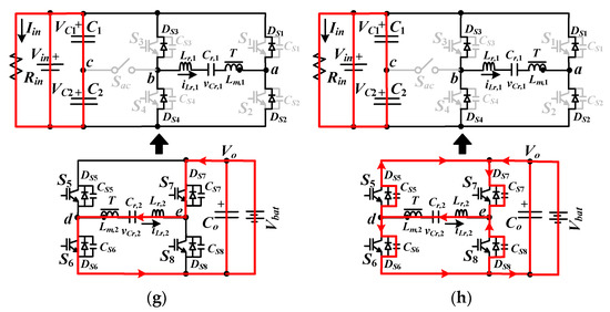
Figure 7.
Equivalent circuits under backward power operation: (a) state 1; (b) state 2; (c) state 3; (d) state 4; (e) state 5; (f) state 6; (g) state 7; (h) state 8.
- State 1 [t0, t1]: At time t0, vCS5 = vCS8 = 0. Owing to iLr,2(t0) < 0, DS5 anf DS8 are conducting. S5 and S8 turn on at this moment to accomplish zero voltage switching. On the left hand side, iLr,1 > 0 and DS1 and DS4 are conducting.
- State 2 [t1, t2]: At time t1, iLr,2 becomes positive and DS5 and DS8 are off. Therefore, the positive current iLr,2 flows through S5 and S8. Power is transferred from Vo to Vin in this state. The leg voltages are Vab = Vin and Vde = Vo. In state 2, the resonant frequency is .
- State 3 [t2, t3]: If fr > fsw, the current iLr,1 will be decreased to 0 at time t2. Then, DS1 and DS4 become off. The resonant frequency in state 3 is expressed as .
- State 4 [t3, t4]: At time t3, S5 and S8 are turned off. The current iLr,2 discharge CS6 and CS7. If the current where iLm,2,peak is the peak value of iLm,2 and CS,2 = CS5 = CS6 = CS7 = CS8, then CS6 and CS7 are discharged to zero voltage.
- State 5 [t4, t5]: At time t4, vCS6 = vCS7 = 0. Owing to iLr,2(t4) > 0, DS6 and DS7 are conducting. S6 and S7 turn on at this moment to realize zero voltage switching. The current iLr,1(t) < 0 and DS2 and DS3 are conducting.
- State 6 [t5, t6]: At time t5, iLr,2 becomes negative and DS6 and DS7 are off. The current iLr,2 flows through S6 and S7. Power is transferred from Vo to Vin in state 6.
- State 7 [t6, t7]: At time t6, iLr,1 = 0 so that DS2 and DS3 are off. The resonant frequency in state 7 is .
- State 8 [t7, Tsw + t0]: At time t7, S6 and S7 are off. The current iLr,2 discharges CS5 and CS8. This switching cycle is ended at time Tsw + t0 when vCS5 = vCS8 = 0.
4. Circuit Analysis and Design Procedures
The presented converter has three operation modes: forward power operation with low-output voltage range, forward power operation with high-output voltage range, and backward power operation as shown in Figure 3, Figure 4, Figure 5 and Figure 6. The frequency modulation is selected to control active devices and regulate load voltage. Therefore, the voltage gain of the presented converter is related to the switching frequency. The equivalent resonant circuits based on the fundamental switching frequency analysis are shown in Figure 8 for three operation modes. For low- and high-output voltage range modes under forward power operation, the input terminal voltages are Vac = ±Vin/2 and Vab = ±Vin, respectively. The root-mean-square leg voltages are expressed as and . The equivalent load resistance Ro,ac at fundamental switching frequency under forward power operation is given as . For backward power operation, the leg voltage Vde = ±Vo and the equivalent resistance Rin,ac at fundamental switching frequency is expressed as . Similarly, the fundamental leg voltage .
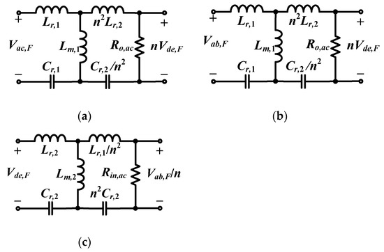
Figure 8.
The equivalent resonant circuits at fundamental switching frequency under (a) low-output voltage range and forward power operation; (b) high-output voltage range and forward power operation; (c) backward power operation.
In Figure 8, the voltage transfer functions under three operation modes can be derived in Equations (1)–(3).
If the following parameters are defined as , , , , and , then Equations (1)–(3) can be rewritten in Equations (4)–(6) for forward power operation under low-output voltage range, forward power operation under high-output voltage range, and backward power operation, respectively.
One can observe that the voltage transfer functions in Equations (4)–(6) are similar. Figure 9a gives the voltage transfer function under K = 5.
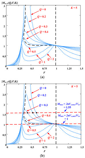
Figure 9.
Gain curves: (a) the proposed converter (b) in the laboratory prototype.
The design procedures of the presented converter are provided in this section to obtain the circuit components in the laboratory prototype. The input voltage Vin = 400 V, the output battery voltage Vo = 200–450 V, the rated power Po,rated = 1 kW, the rated load current Io,rated = 2.3 A, and the resonant frequency fr = 70 kHz. The constant current or constant voltage is selected to charge the battery stack. If the battery stack voltage is in a low voltage range Vo = 200–310 V, the half bridge resonant circuit (Sac on; S3 and S4 off) is operated on the left hand side of the converter. If the output battery stack voltage is in the high voltage range Vo = 310–450 V, the full bridge resonant circuit (Sac off) is operated on the proposed converter to achieve battery charge (forward power operation). For backword power operation (battery discharge from Vo to Vin), the load voltage (Vin) is regulated at 400 V. Since the voltage transfer functions in (4)–(6) have the same circuit characteristics for both forward and backward power operations, the circuit components of the presented converter are derived from forward power operation and low-output voltage range (Vo = 200–310 V). In Equation (4), the voltage gain is related to the output voltage. The high-output voltage will result in large dc voltage gain. In this design example, the assumed minimum voltage gain |Mac,F,Low|min = 1 at Vo,min = 400 V and Vo = 200 V. From Equation (4), the transformer turns ratio n can be expressed in Equation (7).
In this prototype circuit, the selected primary windings (Np) are 90 turns and secondary windings (Ns) are 90 turns. The transformer T is implemented with magnetic core PC40/EE40. According to the selected turn ratio n, the maximum voltage gain in Equation (4) can be obtained as.
Figure 9b illustrates gain curves under K = 5 condition. From the given minimum and maximum dc voltage gains, one can observe the voltage gain |Mac,F,Low| curves under quality factor Q < 0.3 are greater than 1.55. That means the corresponding switching frequency index F can be obtained from Vo,min = 200 V to Vo,max = 310 V to control load voltage. Therefore, Q = 0.3 is used in this design example to obtain the other circuit components. Ro,ac at full load can be derived in Equation (9).
From the given Q and Ro,ac, the primary passive components are derived in Equations (10)–(12).
Then, the secondary resonant components of the proposed converter are obtained as:
The resonant inductors Lr,1 and Lr,2 are implemented with magnetic cores PC40/EER35. Power switches FGH60N60UFD with 600 V/60 A rating are used for switches S1–S8. Power switch 6R125P6 with 650 V/19 A rating is used for switch Sac. The input and output capacitances are C1 = C2 = 2.2 μF/630 V and Co = 660 μF/800 V.
5. Experimental Results
Figure 10a gives the measured load voltage (battery voltage) and load current (battery current). For battery charge, the constant current mode (CC mode) Io = 2.3 A is used to charge the load voltage (battery voltage) from 200 V to 450 V. Then, the constant voltage mode (CV mode) Vo = 450 V is used to charge the battery stack (load) so that the load current is decreased from the rated load current Io = 2.3 A. The measured load voltage Vo = 200 V to 450 V and switch signals vSac and vS3 are given in Figure 10b. When 200 V < Vo < 310 V, Sac is on and S3 is off (half bridge resonant circuit). On the other hand, Sac is off and S3 is triggered by frequency control (full bridge resonant circuit) when 450 V > Vo > 310 V. Figure 11, Figure 12, Figure 13 and Figure 14 give the experimental waveforms of the proposed converter operated at forward power flow. Figure 15 shows the measured waveforms of the proposed converter operated at backward power flow. Figure 11 shows the measured waveforms of the proposed converter operated at Vo = 200 V and the rated load current Io = 2.3 A. Figure 11a gives the measured input voltage, output voltage, and load current. Since the half bridge resonant circuit is operated under Vo = 200 V, the switches S3 and S4 are off and Sac is on. S1 and S2 are controlled with frequency modulation. The measured switch signals of S1 and S2 and the resonant waveforms vCr1 and iLr1 on the primary side are given in Figure 11b. Since the voltage gain of the converter at Vo = 200 V is unity, the switching frequency is close to the resonant frequency. Therefore, the resonant current waveform iLr1 approximates a sinusoidal signal. The measured vCr2, iLr2, iDS5, and iDS7 on the secondary side are provided in Figure 11c. Figure 11d gives the switch voltage and current of S1. One can observe that S1 is turned on at zero voltage so that the turn-on switching loss is eliminated. Figure 12 gives the experimental results of the proposed converter operated at half bridge resonant mode (Figure 3b) under Vo = 310 V and the rated current Io = 2.3 A with constant current mode control. Since the converter has higher voltage gain at Vo = 310 V, the switching frequency is less than the resonant frequency, as shown in Figure 9b. The primary resonant current iLr1 approximates a quasi-sinusoidal waveform (Figure 12b). In Figure 12c, the voltage vCr2 is constant during iLr2 = 0 because no current flows through Cr2. The diodes DS5 and DS7 are turned off at zero current switching. In Figure 12d, S1 is turned on at zero voltage switching. In Figure 13 and Figure 14, the proposed converter is operated at the full bridge resonant circuit (Figure 3c) under Vo = 450 V and Io = 2.3 A and 1.15 A, respectively, with constant voltage mode control. Figure 13b and Figure 14b show the switching signals of S1–S4 under 100% and 50% rated load current. Figure 13c and Figure 14c give the measured leg voltage vab and resonant waveforms vCr1 and iLr1 on the primary side for 100% and 50% rated load current. Similarly, the measured resonant waveforms and diode currents on the secondary side are provided in Figure 13d and Figure 14d. The diodes DS5 and DS7 are turned off at zero current switching. In Figure 13e and Figure 14e, one can observe that S1 is turned on at zero voltage switching for both 100% and 50% rated load current. Figure 15 gives the measured waveforms of the proposed converter operated at backward power operation from Vo = 450 V to Vin = 400 V. Under backward power operation, all switches on the primary side are off and S5–S8 are controlled with frequency modulation. Figure 15a gives the experimental waveforms of Vo, Vin, and Iin at full power condition. Figure 15b shows the switching signals of S5–S8. The leg voltage vde and resonant waveforms vCr2 and iLr2 on the secondary side are measured and provided in Figure 15c. The primary side resonant waveforms iLr1 and vCr1 and diode currents iDS1 and iDS3 are provided in Figure 15d. In Figure 15e, it is clear that S5 is turned on at zero voltage switching. The measured efficiencies of the proposed converter are 92.3%, 93.5%, and 91.5% at Vo = 200 V, 310 V, and 450 V, respectively, under the rated load current with constant current mode control. Figure 16 gives a picture of the prototype circuit. The comparisons between the conventioal dual active bridge converter, CLLC converters, and the studied converter are provided in Table 1. It is clear that two more power switches and split capacitors are used in the proposed circuit. However, more wide output voltage can be operated in the studied circuuit.
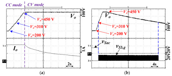
Figure 10.
Measured waveforms (a) Vo and Io under constant current (CC) mode and constant voltage (CV) mode control; (b) Vo, vSac, and vS3,g.
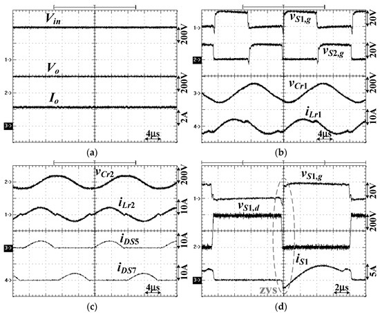
Figure 11.
Experimental waveform of the proposed converter at Vo = 200 V and the rated load current (a) Vin, Vo, and Io; (b) vS1,g, vS2,g, vCr1, and iLr1; (c) vCr2, iLr2, iDS5, and iDS7; (d) vS1,g, vS1,d, and iS1.
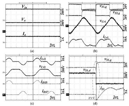
Figure 12.
Experimental waveform of the proposed converter at Vo = 310 V and the rated load current (a) Vin, Vo, and Io; (b) vS1,g, vS2,g, vCr1, and iLr1; (c) iLr2, vCr2, iDS5, and iDS7; (d) vS1,g, vS1,d, and iS1.
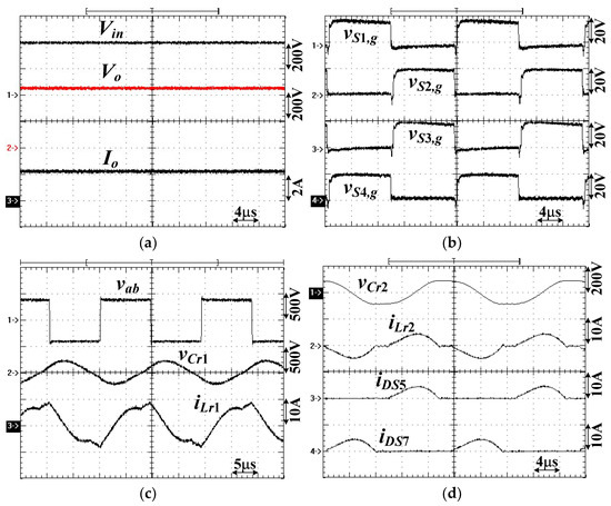
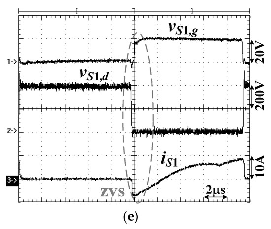
Figure 13.
Experimental waveform of the proposed converter at Vo = 450 V and the rated load current (a) Vin, Vo, and Io; (b) vS1,g–vS4,g; (c) vab, vCr1, and iLr1; (d) vCr2, iLr2, iDS5, and iDS7; (e) vS1,g, vS1,d; and iS1.
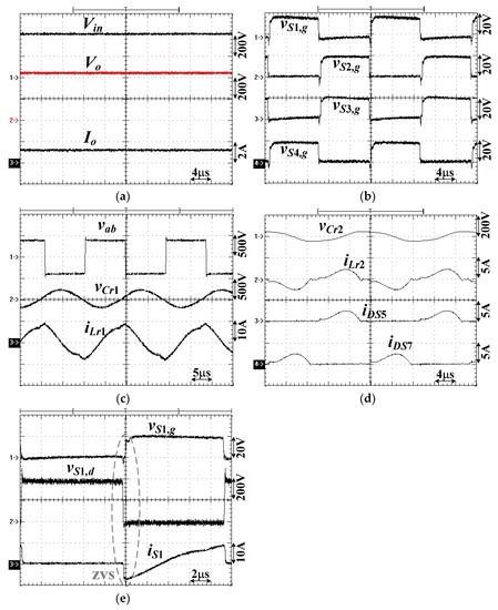
Figure 14.
Experimental waveform of the proposed converter at Vo = 450 V and 50% rated load current (a) Vin, Vo, and Io; (b) vS1,g–vS4,g; (c) vab, vCr1, and iLr1; (d) vCr2, iLr2, iDS5; and iDS7; (e) vS1,g, vS1,d; and iS1.
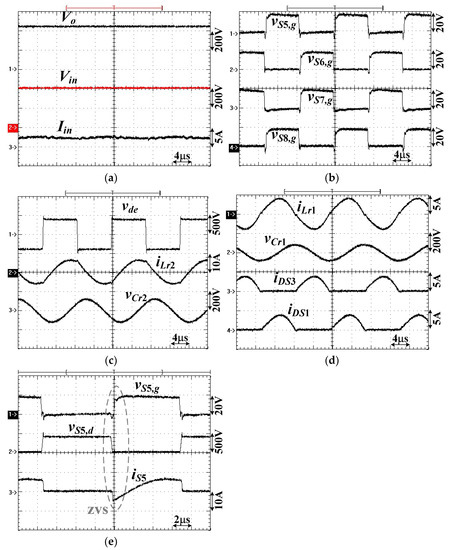
Figure 15.
Experimental waveform of the proposed converter operated at backward power flow from Vo = 450 V to Vin = 400 V under the rated power condition (a) Vo, Vin, and Iin; (b) vS5,g–vS8,g; (c) vde, iLr2, and vCr2; (d) iLr1, vCr1, iDS3, and iDS1; (e) vS5,g, vS5,d, and iS5.
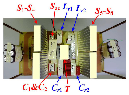
Figure 16.
Picture of the prototype circuit.

Table 1.
Comparisons between DAB converter, CLLC converter, and the studied converter.
6. Conclusions
A bidirectional resonant converter is proposed, analyzed, and implemented for wide voltage range battery charger/discharger applications. The proposed converter can be used between the DC microgrid system and the electric vehicle charge station to realize G2V charge and V2G discharge operations. The proposed converter has symmetric resonant circuits on the primary and secondary sides to realize bidirectional power flow control. By selecting the half bridge or full bridge circuit structure operation, the proposed circuit can achieve low or high voltage gain. Therefore, the wide output voltage control can be implemented in the proposed converter to avoid wide switching frequency variation in conventional bidirectional resonant converters. Due to the resonant circuit behaviors, the power switches are turned on at zero voltage switching so that the switching loss can be reduced. The circuit operation principle, system analysis, circuit characteristics, and design example of the prototype circuit are provided in this paper. The experiments are also provided to validate the performance of the presented converter.
Funding
This research is supported by the National Yunlin University of Science and Technology, Taiwan, under grant number 109H500311.
Institutional Review Board Statement
Not applicable.
Informed Consent Statement
Not applicable.
Acknowledgments
The author thanks the financial support by the National Yunlin University of Science and Technology, Taiwan, under grant number 109H500311. The author would also like to thank Y.-C. Liu for his help to measure and validate the experimental waveforms.
Conflicts of Interest
The authors declare no conflict of interest.
References
- Dragicevic, T.; Lu, X.; Vasquez, J.C.; Guerrero, J.M. DC microgrids—Part I: A review of control strategies and stabilization techniques. IEEE Trans. Power Electron. 2016, 31, 4876–4891. [Google Scholar] [CrossRef] [Green Version]
- Dragicevic, T.; Lu, X.; Vasquez, J.C.; Guerrero, J.M. DC microgrids—Part II: A review of power architectures, applications, and standardization issue. IEEE Trans. Power Electron. 2016, 31, 3528–3549. [Google Scholar] [CrossRef] [Green Version]
- Emadi, A.; Lee, Y.J.; Rajashekara, K. Power electronics and motor drives in electric, hybrid electric, and plug-in hybrid electric vehicles. IEEE Trans. Ind. Electron. 2008, 55, 2237–2245. [Google Scholar] [CrossRef]
- Guerrero, J.M.; Loh, P.C.; Lee, T.L.; Chandorkar, M. Advanced control architectures for intelligent microgrids—Part II: Power quality, energy storage, and ac/dc microgrids. IEEE Trans. Ind. Electron. 2013, 60, 1263–1270. [Google Scholar] [CrossRef] [Green Version]
- Meng, L.; Shafiee, Q.; Trecate, G.F.; Karimi, H.; Fulwani, D.; Lu, X.; Guerrero, J.M. Review on control of DC microgrids and multiple microgrid clusters. IEEE J. Emerg. Sel. Top. Power Electron. 2017, 5, 928–948. [Google Scholar]
- Mangu, B.; Akshatha, S.; Suryanarayana, D.; Fernandes, B.G. Grid-connected PV-wind-battery-based multi-input transformer-couple bidirectional dc-dc converter for household applications. IEEE J. Emerg. Sel. Top. Power Electron. 2016, 4, 1086–1095. [Google Scholar] [CrossRef]
- Yilmaz, M.; Krein, P.T. Review of battery charger topologies, charging power levels, and infrastructure for plug-in electric and hybrid vehicles. IEEE Trans. Power Electron. 2013, 28, 2151–2169. [Google Scholar] [CrossRef]
- Ahrabi, R.R.; Ardi, H.; Elmi, M.; Ajami, A. A novel step-up multi input dc-dc converter for hybrid electric vehicles application. IEEE Trans. Power Electron. 2017, 32, 3549–3561. [Google Scholar] [CrossRef]
- Xu, D.; Zhao, C.; Fan, H. A PWM plus phase-shift control bidirectional DC-DC converter. IEEE Trans. Power Electron. 2004, 19, 666–675. [Google Scholar] [CrossRef]
- Tao, H.; Kotsopoulos, A.; Duarte, J.L.; Hendrix, M.A.M. Family of multiport bidirectional DC-DC converters. IEE Proc. Electr. Power Appl. 2006, 153, 451–458. [Google Scholar] [CrossRef] [Green Version]
- Jain, A.K.; Ayyanar, R. PWM control of dual active bridge: Comprehensive analysis and experimental verification. IEEE Trans. Power Electron. 2011, 26, 1215–1227. [Google Scholar] [CrossRef]
- Zhao, B.; Song, Q.; Liu, W.; Sun, Y. Overview of dual-active-bridge isolated bidirectional DC–DC converter for high-frequency-link power-conversion system. IEEE Trans. Power Electron. 2014, 29, 4091–4106. [Google Scholar] [CrossRef]
- Rico, S.J.; Pagano, D.J.; Lucas, K.E. Bidirectional power sharing for DC microgrid enabled by dual active bridge DC-DC converter. Energies 2021, 14, 404. [Google Scholar]
- Lara, J.; Masisi, L.; Hernandez, C.; Arjona, A.; Chandra, A. Novel five-level ANPC bidirectional converter for power quality enhancement during G2V/V2G operation of cascaded EV charger. Energies 2021, 14, 2650. [Google Scholar] [CrossRef]
- Jung, J.H.; Kim, H.S.; Ryu, M.H.; Baek, J.W. Design methodology of bidirectional CLLC resonant converter for high-frequency isolation of DC distribution systems. IEEE Trans. Power Electron. 2013, 28, 1741–1755. [Google Scholar] [CrossRef]
- Zou, S.; Lu, J.; Mallik, A.; Khaligh, A. Bi-directional CLLC converter with synchronous rectification for plug-in electric vehicles. IEEE Trans. Ind. Appl. 2018, 54, 998–1005. [Google Scholar] [CrossRef]
- Lin, B.R. Analysis of a series-parallel resonant converter for DC microgrid applications. Processes 2021, 9, 542. [Google Scholar] [CrossRef]
- Lin, B.R. Analysis and implementation of a frequency control DC-DC converter for light electric vehicle applications. Electronics 2021, 10, 1623. [Google Scholar] [CrossRef]
Publisher’s Note: MDPI stays neutral with regard to jurisdictional claims in published maps and institutional affiliations. |
© 2021 by the author. Licensee MDPI, Basel, Switzerland. This article is an open access article distributed under the terms and conditions of the Creative Commons Attribution (CC BY) license (https://creativecommons.org/licenses/by/4.0/).