Article

Investigation of Effects of Copper, Zinc, and Strontium Doping on Electrochemical Properties of Titania Nanotube Arrays for Neural Interface Applications

1
Institute for Intelligent Systems Research and Innovation, Deakin University, Waurn Ponds, VIC 3216, Australia
2
Australian Animal Health Laboratory—CSIRO, East Geelong, VIC 3219, Australia
3
Department of Materials Science and Engineering, Case Western Reserve University, Cleveland, OH 44106, USA
4
Centre for Materials and Surface Science, La Trobe University, Bundoora, VIC 3086, Australia
5
School of Material Sciences and Engineering, Georgia Institute of Technology, Atlanta, GA 30332, USA
*
Author to whom correspondence should be addressed.
Processes 2021, 9(12), 2099; https://doi.org/10.3390/pr9122099
Submission received: 15 September 2021 / Revised: 8 November 2021 / Accepted: 11 November 2021 / Published: 23 November 2021
(This article belongs to the Special Issue Novel Electrode Materials for Electrochemical Applications)

Abstract

:
Direct interaction with the neuronal cells is a prerequisite to deciphering useful information in understanding the underlying causes of diseases and functional abnormalities in the brain. Precisely fabricated nanoelectrodes provide the capability to interact with the brain in its natural habitat without compromising its functional integrity. Yet, challenges exist in terms of the high cost and complexity of fabrication as well as poor control over the chemical composition and geometries at the nanoscale, all imposed by inherent limitations of current micro/nanofabrication techniques. In this work, we report on electrochemical fabrication and optimization of vertically oriented TiO2 nanotube arrays as nanoelectrodes for neural interface application. The effects of zinc, strontium, and copper doping on the structural, electrochemical, and biocompatibility properties of electrochemically anodized TiO2 nanotube arrays were investigated. It was found that doping can alter the geometric features, i.e., the length, diameter, and wall thickness, of the nanotubes. Among pure and doped samples, the 0.02 M copper-doped TiO2 nanotubes exhibited superior electrochemical properties, with the highest specific storage capacitance of 130 F g−1 and the lowest impedance of 0.295 KΩ. In addition, regeneration of Vero cells and neurons was highly promoted on (0.02 M) Cu-doped TiO2 nanotube arrays, with relatively small tube diameters and more hydrophilicity, compared with the other two types of dopants. Our results suggest that in situ doping is a promising method for the optimization of various structural and compositional properties of electrochemically anodized nanotube arrays and improvement of their functionality as a potential nanoelectrode platform for neural interfacing.

1. Introduction

Understanding the dynamics and complexity of the brain functions at the neural cell level is one of the main challenges of neuroscience. To this end, previous works have demonstrated a promising approach to precisely recording neural activities over a wide range of brain circuits based on implanting multi-electrode array devices [1]. For neural stimulation, electrodes should be capable of injecting relatively large currents with minimum electrode degradation resulting from faradic effects. This can be achieved by increasing the electrode size, which is often accompanied by a negative impact on the biocompatibility. For long-term stimulation, a large surface area of the electrode is required to facilitate charge transport and reduce inflammatory reaction and gliosis [2]. The nanoscale dimensions of neuron elements such as the cytoskeleton, ionic channels, and filopodia make materials with nanostructures the most suitable architectures to accommodate these features [3,4]. Considerable research has been focused on the employment of high-density interfaces, such as vertical nanoelectrodes, due to the large-scale intracellular recording capability and longer-term intracellular access that arise from their unique geometry. To this end, nanowires of platinum, gold, and gallium phosphide have been used to record electrical activities from neural systems [5,6,7]. Heo et al. have shown stable neural signal recording using polyimide nanofibers [8]. Vertically aligned carbon nanofibers have been developed as a neural chip to stimulate and monitor electrical signals from brain tissue [9].
In this regard, nanomaterial-based approaches for improving electrode functions as well as their biological response have received considerable attention. Among various morphologies of vertical nanoelectrodes, vertically oriented nanotube arrays have shown great potential for the next generation of electrodes for neural interface applications. This outstanding progress is made possible by the unique geometry of the vertically oriented nanotube arrays as well as their one-dimensional pore structure with a high surface area, which promotes cell–electrode electrochemical coupling and provides prolonged access to the cell interior [10]. Previous observations have shown that cell membranes have a tendency to wrap around the nano-objects and protrude outward into nanoholes as small as 100 nm diameter [11].
Among different materials of similar morphologies, nanotubes of a narrow range of materials limited to iridium oxide and carbon have been employed for the application of neural interfacing [2,10,12]. High electrochemical impedance, toxicity, and fabrication complexity are the main limitations of metal oxide nanotubes hindering their use in neural interface application [13,14]. Vertically oriented TiO2 nanotube arrays have been widely studied as a promising biocompatible material for a broad range of biomedical applications [15,16,17]. Several recent publications have suggested TiO2 nanotubes as a favorable material for orthopedic and dental implants as well as drug delivery membranes [18,19]. In vitro studies by Camargo et al. demonstrated that titania nanotubes topography can enhance human osteoblast proliferation and reduce biofilm adhesion, as such promoting bone–titanium integration [20]. While no cytotoxicity effects were outlined in this report, a strong correlation between cell adhesion and growth vs. cell differentiation and nanotube dimensions has been found in other studies, as evidenced by Oh et al. [21].
A comprehensive study by Park et al. identified a narrow window for the optimized nanosize-dependent responses of several cell types (including endothelial cells and mesenchymal stem cells) to TiO2 nanotubes in terms of adhesion, proliferation, differentiation, migration, and apoptosis [22]. These results show the importance of the investigation of combined effects from topography, morphology, and surface chemistry on cellular responses and proposing strategies for the modulation of these properties for successful in vivo applications.
Despite many types of nanotube structures reported in the literature, a limited subset of material compositions has been investigated for the application of nanotubular arrays in neural interfacing due to several limitations. For instance, the high impedance and low charge storage capacitance of TiO2 nanotubes limit their use as electrodes in neural interfacing. Tube morphology has been pointed out as a crucial factor affecting the electrochemical properties and biocompatibility of TiO2 nanotubes [13]. Furthermore, doping with metallic and non-metallic elements has been employed to improve the biocompatibility of TiO2 nanotube arrays [16,23]. For some non-medical applications, such as photocatalysis and dye-sensitized and solar cells, annealing and doping with various types of elements have been employed to enhance the electrochemical properties of nanotube arrays [24,25]. In addition to titania, zinc oxide (ZnO) nanostructures have attracted much attention in the field of biomaterials due to their biocompatibility, as well as the low cost of their fabrication [26,27]. Previous studies have also shown that doping with strontium significantly improves the biological and electrochemical properties of TiO2 nanotubes [28,29]. Copper doping has shown to improve cell regeneration in glass ceramics and increase the hydrophilicity of TiO2 nanotube arrays [30,31]. However, tailoring the structure of TiO2 to achieve a combination of low electrochemical impedance, high-charge storage capacitance, and good biocompatibility remains challenging. Moreover, there is limited research on the application of nanotube arrays for neural microelectrodes. Previous reports have mostly focused on the development and implementation of a limited number of individual nanotubes made by microfabrication-based techniques. In this work, we report on the fabrication and optimization of vertically oriented nanotube arrays of doped titania as a potential electrode platform for parallel electrical interfacing to neurons. High-density vertically oriented titanium oxide nanotube arrays with improved properties have been made using electrochemical anodization technique as a superior approach to the existing microfabrication-based techniques because it gives more control over geometry and chemical composition, feasibility, and versatility in the fabrication of inorganic nanotube structures. The effects of zinc, strontium, and copper doping on the structure and electrochemical properties of TiO2 nanotube arrays were studied. In addition, the wettability and biocompatibility of the doped TiO2 nanotube arrays were evaluated using contact angle measurements and cell culture tests. The results of this work suggest that Cu-doped TiO2 nanotube arrays, with the obtained superior electrochemical and biological performance, can be used as a promising candidate electrode material for application in neural interfaces.

2. Materials and Methods

2.1. Fabrication of Nanotube Arrays

To prepare TiO2 nanotube arrays, pure titanium (Ti) foils (1.5 cm × 1 cm × 50 µm, Sigma Aldrich, Darmstadt, Germany, purity 99.7%) were ultrasonically cleaned with acetone, ethanol, and deionized (D.I.) water for 10 min. The cleaned foils were subjected to a constant voltage of 40 V in an electrochemical anodization setup with two electrodes. Foils of titanium served as anode, and a standard platinum electrode was used as the cathode. The cathode and the anode were separated by a distance of 2 cm. The electrolyte used for the anodization of pure TiO2 nanotubes was prepared by dissolving 0.5 g of ammonium fluoride (NH4F, 98% Sigma Aldrich) in 4 mL of D.I. water and mixing with 94 mL of ethylene glycol (EG, anhydrous, Sigma Aldrich 99.8%).
In situ doping was performed during the electrochemical anodization process. Using the same procedure as above, the zinc, strontium, and copper-doped titania (i.e., Zn-doped, Sr-doped, and Cu-doped TiO2) nanotube arrays were fabricated by preparing separate batches of 0.01 M zinc nitrate (Zn(NO3)2), 0.06 M strontium hydroxide (Sr(OH)2), and different concentrations (0.01 M, 0.02 M, and 0.03 M) of copper nitrate (Cu(NO3)2) electrolytes, respectively. This was done by dissolving 0.12 g of Zn(NO3)2; 0.58 g of Sr(OH)2; and 0.12, 0.24, and 0.37 g of Cu(NO3)2, respectively, in 4 mL of D.I. water containing NH4F. In situ doping was performed during anodization and under the same conditions (i.e., 40 V, 1 h) used for the preparation of pure nanotube arrays. Pure and doped nanotube samples were annealed at 500 °C at a heating rate of 4 °C/min for 3 h in an atmosphere of nitrogen using a tube furnace (Tetlow furnaces, with an FP93 controller/programmer).

2.2. Characterization of the Annealed Nanotube Arrays

The morphology of fabricated TiO2 nanotubes was characterized using ultra-high-resolution field emission scanning electron microscopy (FE-SEM, Carl Zeiss SUPRA®, Cambridge, UK). The inner diameters of 10 nanotubes were measured for each sample using ImageJ software, and the mean value was calculated. The crystal structure was investigated by X-ray diffraction (XRD, Panalytical X-Pert Pro MRD XL, CuKα radiation, λ = 1.5418 Å). Surface elemental analysis was carried out using X-ray photoelectron spectroscopy (XPS) by the Kratos AXIS Nova instrument (Kratos Analytical Ltd., Manchester, UK) equipped with a monochromated Al Kα radiation source (1486.69 eV) operating at 150 W power (15 kV, 10 mA) on an area of ~300 µm × 700 µm. To identify the elemental composition, survey spectra were obtained at 160 eV pass energy. Pass energy of 20 eV was applied to collect high-resolution spectra to identify the oxidation states.

2.3. Electrochemical Properties of the Fabricated Nanotube Arrays

Electrochemical impedance spectroscopy (EIS) and cyclic voltammetry (CV) tests were performed on TiO2 nanotubes in a three-electrode setup using a potentiostat (Bio-Logic Science Instruments, Model VSP, Knoxville, TN, USA). The nanotube film on the titanium substrate as a working electrode, a platinum standard electrode as a counter electrode, and a saturated Ag/AgCl electrode as a reference electrode were used in a potassium buffered saline solution (3 M, KCl). For data acquisition and analysis, the software Bio-Logic EC-lab was used. Bode plots were used to identify electrochemical impedance. CV of the nanotubes was performed under an applied voltage range of –100 to 600 mV versus an Ag/AgCl reference electrode. CV of the fabricated samples was conducted at a scanning rate of 100 mV/s in an electrolyte of 3 M KCl. The sample area under test was 4.9 mm2 in all electrochemical experiments, which was obtained by calculating the circular area of the exposed region. The electrochemical measurements were repeated three times for each sample.

2.4. Contact Angle Measurements

Static contact angle measurements were carried out on the fabricated nanotube films by an optical contact angle meter (Cam 200, KSV Instruments Ltd., Espoo, Finland) using water droplets with a volume of ∼3 mL on every sample at room temperature and in an ambient atmosphere to evaluate the wettability of the nanotube films. A droplet size in the range of 1–10 μL is commonly used for the measuring contact angle. Previous studies show that a droplet size within this range has no significant effect on the contact angle value for smooth, rigid, and non-reactive surfaces [32]. Photos were captured to record the images of the water drops. The contact angles of the water droplets on the nanotube samples were measured in the recorded images using the KSV-Cam software (five repeats for each sample).

2.5. Vero Cell Culture on the Fabricated Nanotube Arrays

Cytotoxicity studies were performed using Vero cells. The Vero lineage was isolated from kidney epithelial cells extracted from an African green monkey (ATCC CCL-81). The use of Vero cells to characterize the biocompatibility of materials is a well-established practice in materials science. This is due to the fact that Vero cells are considered to be one of the most suitable cells for cytotoxicity studies and for the analysis of cell–substrate interactions in biomaterial research [31,33]. For sterilization, nanotube samples were individualized in a 2 mL glass tube, heated in an autoclave for 45 min at 121 °C, and dried by an air gun. The coating process included implementing 200 µL of polyethyleneimine for 30 min. Then, samples were rinsed three times with tissue-culture-grade water. The rinsed samples were treated with laminin by spreading 50 µL of laminin on each sample surface. Then, the samples were placed in an incubator with 5% CO2 for 30 min at 37 °C. After removing the residue laminin, Vero cells were seeded by adding 1 mL of media solution to the surface of each sample and allowing it to rest in the incubator for 2, 4, and 7 days. The experiment was repeated three times for each sample, and the standard deviation from each mean value was calculated.

2.6. Mouse Embryo Dissection Procedure

Cortical embryo primary neurons from mouse (Mus musculus) were prepared by the tissue culture laboratory at the Australian Animal Health Laboratory (AAHL-CSIRO) under the permit AEC number 1686. Whole brains were extracted from C57BL/B6 mouse embryos on embryonic day 15 (E15). Cortical neurons from embryos were removed aseptically from the brain by gently removing the meninges in the cold dissection medium Hibernate (Gibco®). To perform enzymatic dissociation, isolated cortex hemispheres were then treated at 37 °C with deoxyribonuclease (DNase) I solution (0.75 mg/mL) and trypsin in Minimal Essential Medium (MEM) (5 mg/mL) for 5–10 min. Then, mechanical dissociation was performed after three washes with the dissection medium by 10 passages through a 10 mL glass pipette. The cell suspension was then centrifuged for 5 min at 100× g and the pellet was re-suspended in a supplemented Neurobasal® culture medium (ThermoFisher®, Waltham, MA, USA). The experiment was repeated three times for each sample, and the standard deviation from each mean value was calculated.

2.7. Cortical Neurons Culture on the Fabricated Nanotube Arrays

Following the same protocol as for the Vero cell culture, cortical neurons were seeded. Samples were sterilized, dried, coated with polyethylenimine (PEI), and rinsed with TC water. Then, laminin was spread over the sample surface. After removing the remaining of laminin, a volume of dissociated neurons from the stock solution was gently added to the samples, without any solution going over the edges. The plate was placed in an incubator with 5% CO2 for 1 h at 37 °C to let the cells adhere to the samples. Each well was then completed with 1 mL of Neurobasal® culture media. An indirect cell count of the neurons growing on the nanotube samples was performed 3 days post seeding.

2.8. Cell Counting

Due to the lack of transparency of the nanotube films, which prevented the observation of the cells under the microscope, an indirect cell counting procedure was performed 2, 4, and 7 days post Vero cells seeding and 3 days post primary neuron seeding on the samples. For that, samples were carefully removed from the well with forceps and rinsed with phosphate-buffered saline (PBS). A volume of 100 µL of Trypsin/EDTA diluted at 1:10 in PBS was added on the samples in a new 24-well plate. The samples were allowed to rest in an incubator for 5 min for enzyme activation. To stop enzyme activity, either 500 µL of Dulbecco’s Modified Eagle’s Medium (DMEM) was added to the Vero cell culture or 100 µL of Neurobasal® media was added to the primary neuron culture. The volumes in the wells were rigorously mixed to detach the cells from the samples.
For cell counting, a volume of 30 µL of the cell solution was taken and counted under the microscope with a hemocytometer for each sample. Using a hand tally counter, cells were counted and the total number of neurons on the samples was estimated by the following equation:
N u m b e r   o f   c e l l s   p e r   m L = n u m b e r   o f   c o u n t e d   c e l l s × d i l u t i o n   f a c t o r × 10 , 000 n u m b e r   o f   s q u a r e s   c o u n t e d   o n   t h e   h e m o c y t o m e t e r

3. Results and Discussion

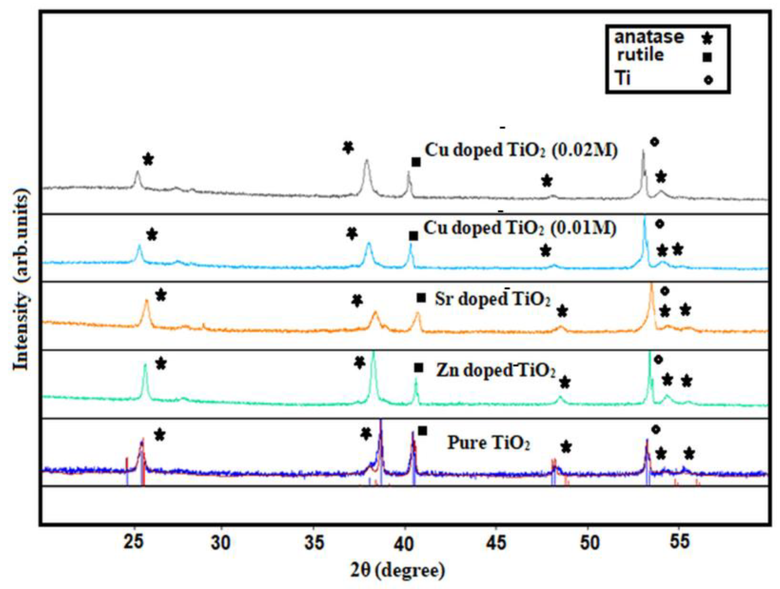
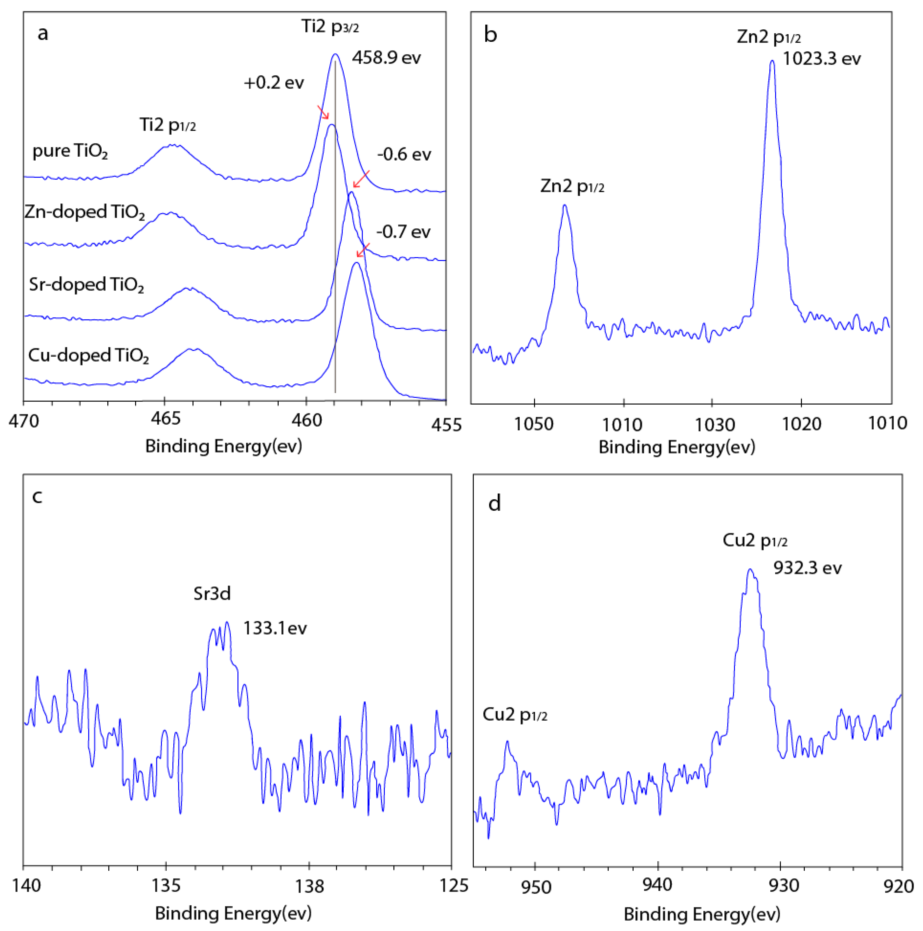
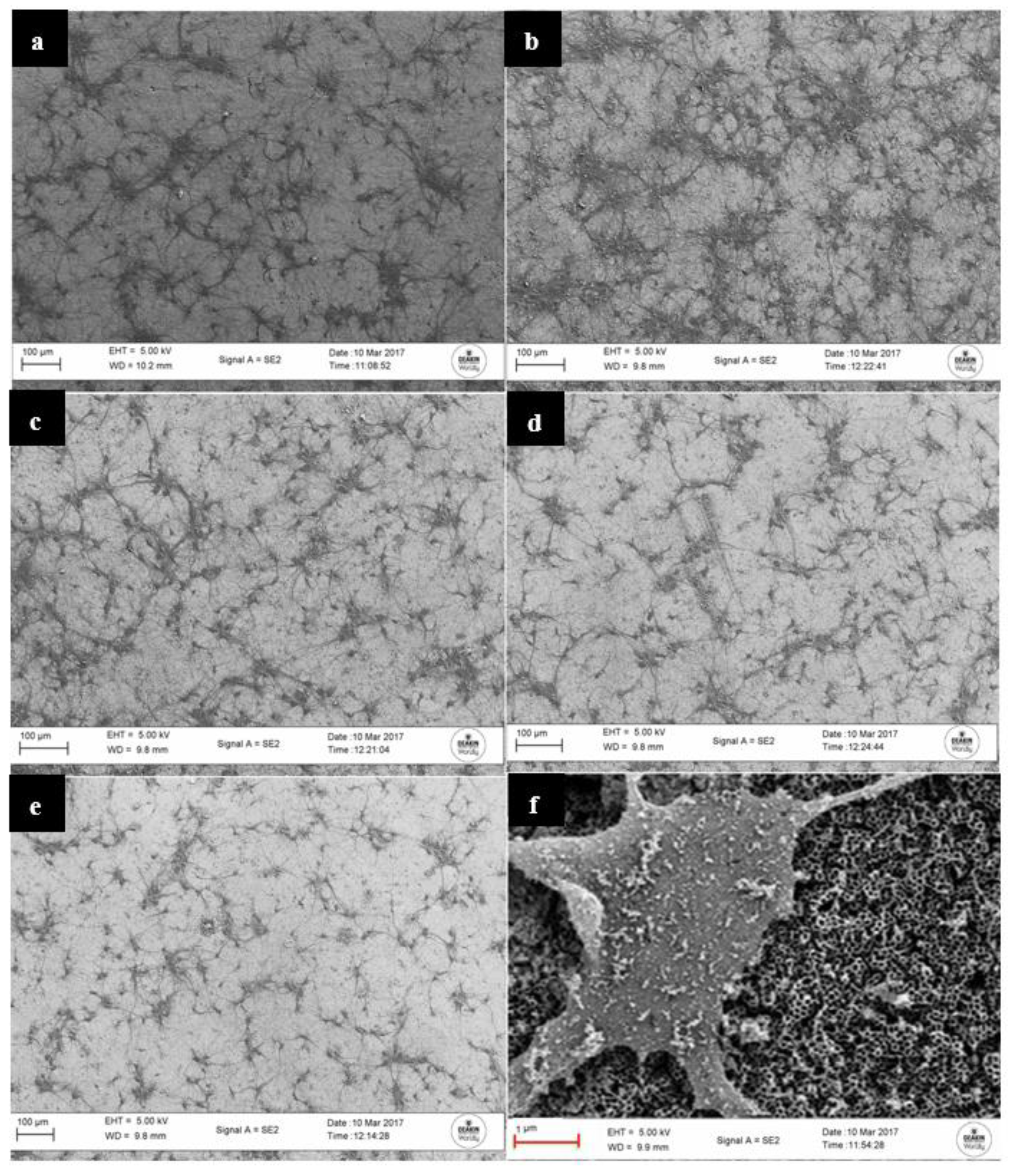
3.1. Structure and Morphology of the Fabricated Nanotube Arrays

Figure 1 shows the top view and cross-sectional SEM images (shown in the insets) of pure (Figure 1a) and doped (Figure 2) TiO2 nanotube arrays after annealing. It is evident that the fabricated nanotubes are vertically ordered. The nanotube dimensions were measured using the ImageJ software. For pure nanotubes (as-fabricated after annealing), the average tube diameter, tube length, and tube wall thickness are 61 nm, 2.25 µm, and 25 nm, respectively (Figure 1a). Figure 1b shows the top view and cross-sectional SEM images of Zn-doped nanotube arrays. The average tube diameter, tube length, and tube wall thickness of Zn-doped nanotube arrays are 67 nm, 1.1 µ, and 15 nm, respectively. The measurements revealed that zinc doping leads to a slight increase in the tube diameters compared to those of pure nanotubes fabricated at the same voltage, while a significant decrease in the tube length and tube wall thickness was observed.
Top and cross-sectional SEM images of Sr-doped nanotubes are shown in Figure 1c. The average tube diameter, tube length, and tube wall thickness of Sr-doped nanotubes are 67.4 nm, 1.8 µm, and 23 nm, respectively. It was observed that doping of nanotubes with strontium resulted in larger diameters, shorter lengths, and thinner walls compared to those of pure nanotubes. Characterization of the tube morphology of Cu-doped nanotubes revealed that both the tube diameter and the tube length decrease while the tube wall thickness increases after the addition of copper nitrate to the electrolyte. Figure 1d shows the SEM images of Cu-doped nanotube arrays fabricated in an electrolyte containing 0.01 M copper nitrate (Cu-doped TiO2 (0.01 M)). The measurements were found to be 60 nm for the tube diameter, 1.3 µm for the tube length, and 32.2 nm for the tube wall thickness. By increasing the concentration of copper nitrate to 0.02 M in the electrolyte, the average inner tube diameter, tube length, and tube wall thickness changed to approximately 56 nm, 1 µm, and 38 nm, respectively. The top and cross-sectional SEM images of the nanotube arrays fabricated in the electrolyte containing 0.02 M copper nitrate (Cu-doped TiO2 (0.02 M)) are shown in Figure 1e. It was found that increasing the concentration of the copper nitrate to 0.03 M does not lead to the formation of nanotubular arrays (Figure 1f); thus, further studies on 0.03 M Cu-doped samples were not pursued.
To investigate the structure of the doped nanotube arrays after annealing, XRD analysis was performed on the samples. Figure 2 shows the XRD patterns of the fabricated nanotube arrays. The XRD pattern of the annealed nanotubes shows a crystal structure with the anatase phase recognizable by the peaks (and the corresponding crystallographic plane) at 2θ = of 25.418° (101), 38.765° (112), 48.22° (200), 54.344° (105), and 55.292° (211). The peak positions are consistent with the standard powder diffraction data for anatase (JCPDS card #01-070-6826), titanium (JCPDS card #01-071-4632), and rutile (JCPDS) card #00−021−1276). The patterns of the doped nanotube arrays show a clear shift to the lower angles in anatase peaks compared to the pattern of the annealed pure nanotube arrays. This shift is attributed to the strain and disorder in the crystal lattice structure of TiO2 that is generated from the insertion of dopant ions with relatively larger ionic radii (Zn2+ (0.88 Å), Sr2+ (1.32 Å), and Cu2 (0.87 Å)) than that of Ti4+ (0.75 Å) [34].
For chemical state analysis, XPS measurements were performed on pure and doped nanotube arrays. High-resolution spectra of Ti 2p, Zn 2p, Sr 3d, and Cu 2p are displayed in Figure 3. As can be seen in Figure 3a, the Ti 2p3/2 and Ti 2p1/2 peaks of pure nanotubes appear at 458.9 and 464.6 eV, with a spin orbit splitting of 5.7 eV, confirming that both signals correspond to Ti4+ [34]. It was found that doping with Zn ions shifts the Ti 2p peaks to higher binding energies, while these peaks shift to lower binding energies on doping the nanotube arrays with Sr and Cu ions. For the Zn-doped sample, Zn 2p spectra with two peaks were obtained corresponding to the Zn 2p3/2 and Zn 2p1/2 photoemission spectra occurring at the binding energies of 1023 and 1046 eV, respectively. As shown in Figure 3b, the two peaks were separated by 23 eV, which indicates that Zn ions in the form of ZnO clusters are distributed on the surface of TiO2 nanotubes. Similar to previous works, ZnO clusters could not be seen on the SEM images. This could be related to the combination of Ti–O–Zn bonds in the lattice of TiO2 as a result of annealing [25,26]. Figure 3c shows a peak corresponding to the Sr 3d for the Sr-doped sample appearing at the binding energy of 133.1 eV, indicating that strontium has been successfully doped into TiO2 nanotubes. The Sr 3d binding energy corresponded to the energy-level diagram of Sr2+ [28]. Figure 3d shows the Cu 2p spectra at 932.3 eV, which can be related to the existence of Cu2+ in the Cu2O [35].

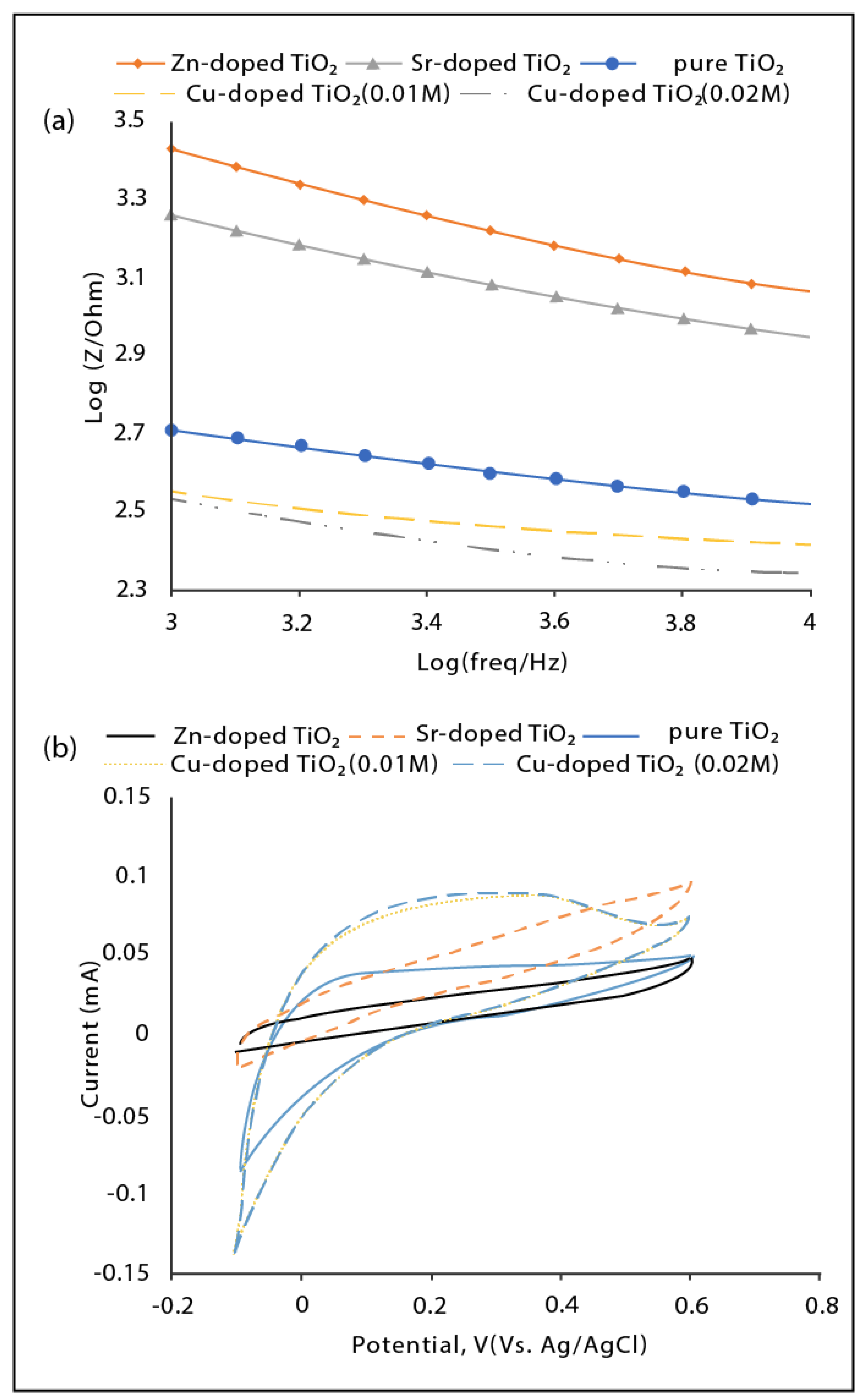
3.2. Electrochemical Performance of the Fabricated Nanotube Arrays

To investigate their electrochemical properties, pure and doped nanotube arrays were subjected to electrochemical impedance spectroscopy (EIS) and cyclic voltammetry (CV) tests after annealing. Figure 4a shows Bode plots of fabricated nanotube arrays. The measurement revealed that pure nanotube arrays have an impedance value of 0.501 kΩ. Doping with zinc increased the impedance of resultant nanotube arrays to 2.7 kΩ. The increase in the nanotube impedance could be related to two possible reasons; the first one can be attributed to the tube wall thickness. Zn-doped TiO2 nanotubes have thinner walls than those of pure nanotubes. Previous studies have shown that tubes with thicker walls are more conductive than those of thinner ones [18]. The second possible reason can be related to the presence of zinc oxide, which has high electrical resistance, resulting in a decrease in the electrical conductivity of the nanotube arrays [36].
The EIS results of Sr-doped nanotube arrays showed lower impedance than that of Zn-doped TiO2 arrays (1.7 KΩ), but they are still less conductive than the pure nanotubes. Thicker walls of pure nanotubes improve charge transport and reduce the impedance. Furthermore, Sr2+ ions can substitute for Ti4+ in the lattice of TiO2 and in addition to Ti4+ sites, the large-size strontium ions occupy oxygen vacancies adjacent to the substitutional sites [34]. Chao et al. showed that a dominant conduction mechanism for fine-grain TiO2 is via long-range migration of oxygen vacancies [37]. The occupation of these sites can lead to an increase in the impedance of TiO2 nanotube arrays.
From Figure 4a, it can be seen that the electrochemical impedance of the TiO2 nanotube arrays is significantly decreased after Cu doping. Impedance values decreased from 0.501 KΩ for pure TiO2 nanotubes to 0.331 and 0.295 KΩ for 0.01 and 0.02 M Cu doping, respectively. The decrease in impedance values could be attributed to morphological and structural effects. Cu-doped nanotubes have much shorter lengths and thicker walls than those of pure nanotubes. The observed trend seems logical considering that electrical resistance has a direct relationship with tube length and an inverse relationship with cross-section area [38,39]. Moreover, random substitution of Cu2+ ions in the lattice of TiO2 can contribute to conductivity enhancement. As Cu2+ is a highly conductive ion, the presence of such ions in the tube walls provides a path with less impedance for charge transfer compared to the tube walls of copper-free TiO2 nanotube arrays [40]. It was observed that increasing the concentration of copper nitrate in the electrolyte from 0.01 to 0.02 M leads to a slight increase in the conductivity of the resultant nanotubes, possibly due to the slight increase in the tube wall thickness, slight decrease in the tube length, and more incorporation of Cu ions in the structure of TiO2.
To estimate charge storage capacitance, cyclic voltammetry measurements were performed on the fabricated nanotube arrays. Figure 4b shows the cyclic voltammetry curves of pure, Zn-doped, Sr-doped, and Cu-doped TiO2 nanotube arrays. It was found that charge storage capacitance is inversely proportional to impedance. Higher capacitance is for more conductive nanotubes (less electrochemical impedance), and this could be related to a low resistance to charge transfer through the charge–discharge process [13]. It is clear from the areas between the charge–discharge curves that 0.02 M Cu-doped TiO2 nanotube arrays have the highest specific storage capacitance of 130 F g−1. Inversely proportional to the impedance of the nanotube arrays, the specific capacitance values were 125, 94.85, 45, and 40 F g−1 for 0.01 M Cu-doped TiO2, pure TiO2, Sr-doped TiO2, and Zn-doped TiO2, respectively. This is in accordance with our observations above on the inverse relationship between impedance and the density of oxygen vacancies and the findings of Salari et al. that partial-oxygen-depleted titania (i.e., with more oxygen vacancies) has a higher capacitance and is more conductive than titania with fewer oxygen vacancies [41].

3.3. Wettability of the Fabricated Nanotube Arrays

To estimate the wettability of the doped nanotube arrays, water contact angles were measured for pure, Zn-doped, Sr-doped, and Cu-doped TiO2 nanotube arrays. The chart in Figure 5 shows the static water contact angles of the water droplets on the surfaces of the pure and doped TiO2 nanotube arrays with their corresponding images of the water droplets on the samples shown on top. Except for Zn-doped TiO2 nanotubes (θ > 90°), all samples showed a hydrophilic property (θ < 90°). Cu-doped nanotube arrays (0.02 M) exhibited the highest hydrophilicity. This can be due to more oxygen vacancies induced in the lattice of TiO2 by doping with Cu2+ ions. These vacancies are favorable sites for occupation by water molecules; this enables the rapid spread of water on the surface [29]. Sr-doped nanotube arrays showed lower hydrophilicity than Cu-doped arrays. This may be due to the smaller tube diameters of Cu-doped nanotubes and the higher crystallinity of Cu-doped nanotube arrays. With the relatively large tube diameters, Zn-doped nanotubes showed the most hydrophobic behavior with the largest contact angle. As mentioned earlier, Zn may exist as ZnO in the structure of Zn-doped TiO2. Previous studies have pointed out that ZnO shows superhydrophobicity, which may cause a significant reduction in the wettability of TiO2 nanotube arrays [42].

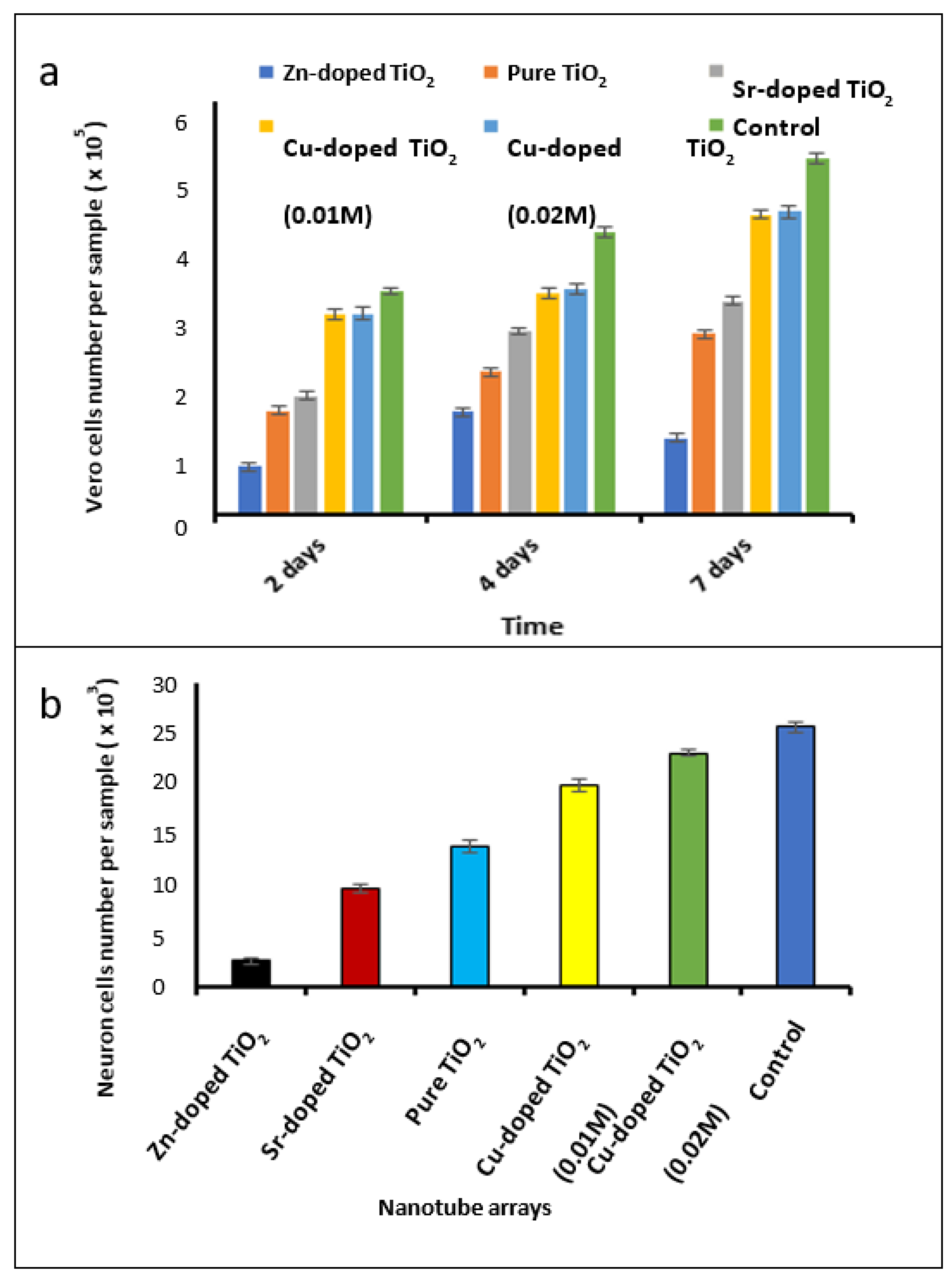
3.4. Investigation of Biocompatibility of the Fabricated Nanotube Arrays

For evaluation of the biocompatibility of anodized nanotube arrays, Vero cells were cultured on the surfaces of pure and doped samples after annealing. Vero cells were grown on the surfaces of the samples at the initial density of 10,000 cells/sample. Cell proliferation as estimated by counting of cell numbers after 2, 4, and 7 days was found to be the highest on Cu-doped nanotube arrays (Figure 6a) after control. Control refers to the cell culture in its standard culturing conditions on a Petri dish. The superior performance of Cu-doped nanotubes in terms of the regeneration of Vero cells could be attributed to their relatively small tube diameters and higher hydrophilicity. It has been previously reported that nanotubes with smaller diameters are more biocompatible than those with larger diameters [22,43]. In addition, it has been previously demonstrated that the presence of Cu ions in the lattice of TiO2 nanotubes enhances cell regeneration [30]. Cell counting showed that cell proliferation on Cu-doped TiO2 arrays (0.01 M) is higher than that of Cu-doped TiO2 arrays (0.01 M) as the former have smaller tube diameters and more contributions from Cu2+ ions.
Sr-doped and Zn-doped TiO2 nanotube arrays have relatively similar tube diameters, while Sr-doped TiO2 nanotubes show more support to cell regeneration, indicating that the presence of strontium in the tubes has a greater effect on the cell growth. Although many previous studies have pointed out that strontium doping enhances cell growth on TiO2 nanotube arrays, more cell growth on pure TiO2 nanotube was noticed in this study, pointing to the dominating effect of tube diameter, as pure nanotubes have smaller diameters than those of Sr-doped nanotubes.
To observe the effect of doping on TiO2 nanotube arrays for the application of neural interfacing, neurons were cultured on the pure and doped nanotube arrays after annealing to evaluate the biocompatibility of doped nanotubes with the cultured neurons. Figure 6b shows the neuron numbers counted on fabricated nanotube arrays. Neurons with an initial number of 25,000 were cultured for 3 days. Doped nanotube arrays showed similar effects on the neurons as what was observed on the Vero cells. A previous study demonstrated that neurons show better growth on more conductive TiO2 nanotubes [44]. The results of our research are in line with this data. The largest number of neurons were found on Cu-doped TiO2 (0.02 M) nanotubes, which have the highest electrical conductivity among the fabricated arrays in this work. However, Zn-doped TiO2 nanotubes, which have the lowest electrical conductivity, showed less support to cell growth than other doped nanotubes. To support these findings, the growth of neurons on the sample surfaces was inspected by SEM (Figure 7a–e). ImageJ software was used to estimate the surface areas of the samples that were covered by the neurons. The measurements showed that neurons cover about 46%, 43%, 35%, 30%, and 22% of the sample surfaces of Cu-doped TiO2 (0.02 M), Cu-doped TiO2 (0.01 M), pure TiO2, Sr-doped TiO2, and Zn-doped TiO2 nanotube arrays, respectively. The higher-magnification SEM image of Cu-doped TiO2 (0.02 M) nanotube arrays shown in Figure 7f confirms direct attachment of a single neuron to the nanotubes. The observed largest density of neurons (46%) on the Cu-doped TiO2 (0.02 M) nanotube arrays reveals a favorable interaction between these nanotubes and the neurons arising from a combination of composition and geometric characteristics of this sample. In other words, this combined effect is in favor of promoting direct neuronal adhesion onto the nanotubes, which could result in improving recording resolution and stability and the overall performance of the neural interface device.

4. Conclusions

This paper reports the effect of doping on the structure, electrochemical properties, and biocompatibility of titania nanotube arrays for neural interface applications. Vertically oriented pure and doped TiO2 nanotube arrays were fabricated via electrochemical anodization following in situ doping with zinc, strontium, and copper, separately, during anodization. Results show that the geometric characteristics of the nanotube arrays (i.e., their length, diameter, and wall thickness) can be modified via doping, which combined with the changes in their chemical composition results in the observed differences in their electrochemical and biocompatibility properties. EIS analysis revealed the highest specific storage capacitance of 130 F g−1 and the lowest impedance of 0.295 KΩ in (0.02 M) Cu-doped TiO2 nanotube arrays. In addition, the regeneration of Vero cells and neurons was highly promoted on (0.02 M) Cu-doped TiO2 nanotube arrays with relatively small tube diameters and more hydrophilicity among the three types of dopants. Such improvements in the properties of TiO2 nanotube arrays make them a promising candidate electrode material architecture for the next generation of neural interfaces.

Author Contributions

Conceptualization, D.K., A.B. (Asim Bhatti), H.A.H.; methodology, D.K., A.B.; formal analysis, D.K., J.G., A.B. (Anders Barlow); investigation, D.K., J.G., H.A.H.; writing—original draft preparation, D.K., A.B. (Asim Bhatti), H.A.H.; writing—review and editing, D.K., A.B. (Asim Bhatti), H.A.H., H.G.; visualization, D.K., H.A.H.; supervision, A.B. (Asim Bhatti); project administration, A.B. (Asim Bhatti); All authors have read and agreed to the published version of the manuscript.

Funding

This research received no external funding.

Institutional Review Board Statement

All biological investigations were conducted by the tissue culture laboratory at the Australian Animal Health Laboratory (AAHL-CSIRO) under the permit AEC number 1686.

Informed Consent Statement

Not applicable.

Data Availability Statement

Not applicable.

Acknowledgments

The content of this manuscript has been published in part as part of the thesis of Dhurgham Ismael Khudhair, “Nano electrode based on TiO2 nanotubes for neural interfacing”, Deakin University, Institute for Intelligent Systems Research and Innovation, Victoria, Australia 2018.

Conflicts of Interest

The authors declare no conflict of interest.

References

  1. Angotzi, G.N.; Boi, F.; Lecomte, A.; Miele, E.; Malerba, M.; Zucca, S.; Casile, A.; Berdondini, L. Sinaps: An implantable active pixel sensor CMOS-probe for simultaneous large-scale neural recordings. Biosens. Bioelectron. 2019, 126, 355–364. [Google Scholar] [CrossRef]
  2. Carli, S.; Lambertini, L.; Zucchini, E.; Ciarpella, F.; Scarpellini, A.; Prato, M.; Castagnola, E.; Fadiga, L.; Ricci, D. Single walled carbon nanohorns composite for neural sensing and stimulation. Sens. Actuators B Chem. 2018, 271, 280–288. [Google Scholar] [CrossRef]
  3. Kotov, N.A.; Winter, J.O.; Clements, I.P.; Jan, E.; Timko, B.P.; Campidelli, S.; Pathak, S.; Mazzatenta, A.; Lieber, C.M.; Prato, M.; et al. Nanomaterials for neural interfaces. Adv. Mater. 2009, 21, 3970–4004. [Google Scholar] [CrossRef] [Green Version]
  4. Khudhair, D.; Nahavandi, S.; Garmestani, H.; Bhatti, A. Microelectrode arrays: Architecture, challenges and engineering solutions. In Emerging Trends in Neuro Engineering and Neural Computation; Springer: Cham, Switzerland, 2017; pp. 41–59. [Google Scholar]
  5. Xie, C.; Lin, Z.; Hanson, L.; Cui, Y.; Cui, B. Intracellular recording of action potentials by nanopillar electroporation. Nat. Nanotechnol. 2012, 7, 185–190. [Google Scholar] [CrossRef] [Green Version]
  6. Brüggemann, D.; Wolfrum, B.; Maybeck, V.; Mourzina, Y.; Jansen, M.; Offenhäusser, A. Nanostructured gold microelectrodes for extracellular recording from electrogenic cells. Nanotechnology 2011, 22, 265104. [Google Scholar] [CrossRef]
  7. Suyatin, D.B.; Wallman, L.; Thelin, J.; Prinz, C.N.; Jörntell, H.; Samuelson, L.; Montelius, L.; Schouenborg, J. Nanowire-based electrode for acute in vivo neural recordings in the brain. PLoS ONE 2013, 8, e56673. [Google Scholar] [CrossRef]
  8. Heo, D.N.; Kim, H.-J.; Lee, Y.J.; Heo, M.; Lee, S.J.; Lee, D.; Do, S.H.; Lee, S.H.; Kwon, I.K. Flexible and highly biocompatible nanofiber-based electrodes for neural surface interfacing. ACS Nano 2017, 11, 2961–2971. [Google Scholar] [CrossRef]
  9. Yu, Z.; McKnight, T.E.; Ericson, M.N.; Melechko, A.V.; Simpson, M.L.; Morrison, B. Vertically aligned carbon nanofiber neural chip for interfacing with neurological system. In Proceedings of the 4th IEEE International Conference on Nano/Molecular Medicine and Engineering (IEEE-NANOMED), Hong Kong, China, 5–9 December 2010; pp. 188–191. [Google Scholar]
  10. Lin, Z.; Xie, C.; Osakada, Y.; Cui, Y.; Cui, B. Iridium oxide nanotube electrodes for sensitive and prolonged intracellular measurement of action potentials. Nat. Commun. 2014, 5, 3206. [Google Scholar] [CrossRef]
  11. Richards, C.I.; Luong, K.; Srinivasan, R.; Turner, S.W.; Dougherty, D.A.; Korlach, J.; Lester, H.A. Live-Cell Imaging of Single Receptor Composition Using Zero-Mode Waveguide Nanostructures. Nano Lett. 2012, 12, 3690–3694. [Google Scholar] [CrossRef] [Green Version]
  12. Wang, K.; Fishman, H.A.; Dai, H.; Harris, J.S. Neural Stimulation with a Carbon Nanotube Microelectrode Array. Nano Lett. 2006, 6, 2043–2048. [Google Scholar] [CrossRef]
  13. Khudhair, D.; Hamedani, H.A.; Gaburro, J.; Shafei, S.; Nahavandi, S.; Garmestani, H.; Bhatti, A. Enhancement of electro-chemical properties of TiO2 nanotubes for biological interfacing. Mater. Sci. Eng. C 2017, 77, 111–120. [Google Scholar] [CrossRef]
  14. Khudhair, D.; Gaburro, J.; Shafei, S.; Barlow, A.; Nahavandi, S.; Bhatti, A. Enhancement of electrochemical properties of micro/nano electrodes based on TiO2 nanotube arrays. J. Phys. Conf. Ser. 2017, 829, 012010. [Google Scholar] [CrossRef]
  15. Grimes, C.A.; Mor, G.K. TiO2 Nanotube Arrays: Synthesis, Properties, and Applications; Springer Science & Business Media: Berlin/Heidelberg, Germany, 2009. [Google Scholar]
  16. Zhou, M.; Glushenkov, A.M.; Kartachova, O.; Li, Y.; Chen, Y. Titanium dioxide nanotube films for electrochemical supercapacitors: Biocompatibility and operation in an electrolyte based on a physiological fluid. J. Electrochem. Soc. 2015, 162, A5065–A5069. [Google Scholar] [CrossRef]
  17. Khudhair, D.; Bhatti, A.; Li, Y.; Hamedani, H.; Garmestani, H.; Hodgson, P.; Nahavandi, S. Anodization parameters influencing the morphology and electrical properties of TiO2 nanotubes for living cell interfacing and investigations. Mater. Sci. Eng. C 2016, 59, 1125–1142. [Google Scholar] [CrossRef]
  18. Shim, S.C.; Choe, B.H.; Jang, I.S.; Choi, D.S.; Lee, J.K.; Cha, B.K.; Choi, W.Y. Effect of TiO2 Nanotube Arrays on Osseointegration for Dental Implant. Adv. Mater. Res. 2014, 922, 71–74. [Google Scholar] [CrossRef]
  19. Lai, Y.-K.; Wang, Q.; Huang, J.-Y.; Li, H.-Q.; Chen, Z.; Zhao, A.Z.-J.; Wang, Y.; Zhang, K.-Q.; Sun, H.-T.; Al-Deyab, S.S. TiO2 nanotube platforms for smart drug delivery: A review. Int. J. Nanomed. 2016, 11, 4819–4834. [Google Scholar] [CrossRef] [Green Version]
  20. Camargo, S.E.A.; Xia, X.; Fares, C.; Ren, F.; Hsu, S.-M.; Budei, D.; Aravindraja, C.; Kesavalu, L.; Esquivel-Upshaw, J.F. Nanostructured Surfaces to Promote Osteoblast Proliferation and Minimize Bacterial Adhesion on Titanium. Materials 2021, 14, 4357. [Google Scholar] [CrossRef]
  21. Oh, S.; Brammer, K.S.; Li, Y.S.J.; Teng, D.; Engler, A.J.; Chien, S.; Jin, S. Stem cell fate dictated solely by altered nanotube dimension. Proc. Natl. Acad. Sci. USA 2009, 106, 2130–2135. [Google Scholar] [CrossRef] [Green Version]
  22. Park, J.; Bauer, S.; Schmuki, P.; von der Mark, K. Narrow Window in Nanoscale Dependent Activation of Endothelial Cell Growth and Differentiation on TiO2 Nanotube Surfaces. Nano Lett. 2009, 9, 3157–3164. [Google Scholar] [CrossRef]
  23. Szkoda, M.; Lisowska-Oleksiak, A.; Siuzdak, K. Optimization of boron-doping process of titania nanotubes via electrochemical method toward enhanced photoactivity. J. Solid State Electrochem. 2016, 20, 1765–1774. [Google Scholar] [CrossRef] [Green Version]
  24. Shikandar, D.; Shetti, N.; Kulkarni, R.; Kulkarni, S. Silver-doped titania modified carbon electrode for electrochemical studies of Furantril. ECS J. Solid State Sci. Technol. 2018, 7, Q3215–Q3220. [Google Scholar] [CrossRef]
  25. Shetti, N.P.; Bukkitgar, S.D.; Kakarla, R.R.; Reddy, C.; Aminabhavi, T.M. ZnO-based nanostructured electrodes for electrochemical sensors and biosensors in biomedical applications. Biosens. Bioelectron. 2019, 141, 111–417. [Google Scholar] [CrossRef]
  26. Bukkitgar, S.D.; Shetti, N.P.; Kulkarni, R.M.; Reddy, K.R.; Shukla, S.S.; Saji, V.S.; Aminabhavi, T.M. Electro-catalytic behavior of Mg-doped ZnO nano-flakes for oxidation of anti-inflammatory drug. J. Electrochem. Soc. 2019, 166, B3072–B3078. [Google Scholar] [CrossRef]
  27. Wang, Y.; Zhang, D.; Wen, C.; Li, Y. Processing and characterization of SrTiO3–TiO2 nanoparticle–nanotube heterostructures on titanium for biomedical applications. ACS Appl. Mater. Interfaces 2015, 7, 16018–16026. [Google Scholar] [CrossRef]
  28. Hamedani, H.A.; Allam, N.K.; Garmestani, H.; El-Sayed, M.A. Electrochemical fabrication of strontium-doped TiO2 nanotube array electrodes and investigation of their photoelectrochemical properties. J. Phys. Chem. C 2011, 115, 13480–13486. [Google Scholar] [CrossRef]
  29. Wang, S.; Meng, K.; Zhao, L.; Jiang, Q.; Lian, J. Superhydrophilic Cu-doped TiO2 thin film for solar-driven photocatalysis. Ceram. Int. 2014, 40, 5107–5110. [Google Scholar] [CrossRef]
  30. Wers, E.; Bunetel, L.; Oudadesse, H.; Lefeuvre, B.; Lucas-Girot, A.; Mostafa, A.; Pellen, P. Effect of Copper and Zinc on the Bioactivity and Cells Viability of Bioactive Glasses. Bioceram. Dev. Appl. 2013, 1–3. [Google Scholar] [CrossRef] [Green Version]
  31. Ghane-Motlagh, B.; Sawan, M. A review of Microelectrode Array technologies: Design and implementation challenges. In Proceedings of the 2nd International Conference on Advances in Biomedical Engineering, Beirut, Lebanon, 11–13 September 2013; pp. 38–41. [Google Scholar]
  32. Shedid, S.A.; Ghannam, M.T. Influences of Droplet Volume on Contact Angle of Reservoir Rocks. Energy Sources 2005, 27, 1085–1097. [Google Scholar] [CrossRef]
  33. Kirkpatrick, C. Biological testing of materials and medical devices-a critical view of current and proposed methodologies for biocompatibility testing: Cytotoxicity in vitro. Regul. Affairs 1992, 4, 13–32. [Google Scholar]
  34. Hamedani, H.A.; Allam, N.K.; El-Sayed, M.A.; Khaleel, M.A.; Garmestani, H.; Alamgir, F.M. An Experimental Insight into the Structural and Electronic Characteristics of Strontium-Doped Titanium Dioxide Nanotube Arrays. Adv. Funct. Mater. 2014, 24, 6783–6796. [Google Scholar] [CrossRef]
  35. Momeni, M.M.; Ghayeb, Y.; Ghonchegi, Z. Fabrication and characterization of copper doped TiO2 nanotube arrays by in situ electrochemical method as efficient visible-light photocatalyst. Ceram. Int. 2015, 41, 8735–8741. [Google Scholar] [CrossRef]
  36. Heckelsberg, L.F.; Calrk, A.; Bailey, G.C. Electrical Conductivity and Catalytic Activity of Zinc Oxide. J. Phys. Chem. 1956, 60, 559–561. [Google Scholar] [CrossRef]
  37. Chao, S.; Petrovsky, V.; Dogan, F. Complex Impedance Study of Fine and Coarse Grain TiO2 Ceramics. J. Am. Ceram. Soc. 2010, 93, 3031–3034. [Google Scholar] [CrossRef]
  38. Xiao, P.; Zhang, Y.; Garcia, B.B.; Sepehri, S.; Liu, D.; Cao, G. Nanostructured electrode with titania nanotube arrays: Fabrication, electrochemical properties, and applications for biosensing. J. Nanosci. Nanotechnol. 2009, 9, 2426–2436. [Google Scholar] [CrossRef]
  39. Sun, L.; Zhang, S.; Sun, X.; He, X. Effect of the geometry of the anodized titania nanotube array on the performance of dye-sensitized solar cells. J. Nanosci. Nanotechnol. 2010, 10, 4551–4561. [Google Scholar] [CrossRef]
  40. Mohajernia, S.; Hejazi, S.; Andryskova, P.; Zoppellaro, G.; Tomanec, O.; Zboril, R.; Schmuki, P. Conductive Cu doped TiO2 nanotubes for enhanced photoelectrochemical methanol oxidation and concomitant hydrogen generation. ChemElectroChem 2019, 6, 1244–1249. [Google Scholar] [CrossRef]
  41. Salari, M.; Konstantinov, K.; Liu, H.K. Enhancement of the capacitance in TiO2 nanotubes through controlled introduction of oxygen vacancies. J. Mater. Chem. 2011, 21, 5128–5133. [Google Scholar] [CrossRef] [Green Version]
  42. Wei, Q.; Wang, S.; Li, W.; Yuan, X.; Bai, Y. Hydrophobic ZnO-TiO2 nanocomposite with photocatalytic promoting self-cleaning surface. Int. J. Photoenergy 2015, 2015, 925638. [Google Scholar] [CrossRef] [Green Version]
  43. Brammer, K.S.; Oh, S.; Frandsen, C.J.; Jin, S. Biomaterials and biotechnology schemes utilizing TiO2 nanotube arrays. Biomater. Sci. Eng. 2011, 193–210. [Google Scholar]
  44. Sorkin, J.A. Titania Nanotube Arrays as Potential Interfaces for Neurological Prostheses. Ph.D. Thesis, Colorado State University, Fort Collins, CO, USA, 2014. [Google Scholar]
Figure 1. Top view SEM images of annealed nanotube arrays (a) pure TiO2, (b) Zn-doped TiO2, (c) Sr-doped TiO2, (d) Cu-doped TiO2 (0.01 M), (e) Cu-doped TiO2 (0.02 M), and (f) Cu-doped TiO2 (0.03 M). The insets show cross-sectional SEM images of the samples. The scale bar is 100 nm.
Processes 09 02099 g001
Figure 2. XRD patterns of pure and doped TiO2 nanotube arrays after annealing.
Processes 09 02099 g002
Figure 3. High-resolution XPS spectra of pure and doped TiO2 nanotube arrays after annealing. (a) Ti 2p in pure and doped TiO2 nanotube samples, (b) Zn 2p spectrum of Zn-doped TiO2, (c) Sr 3d spectrum of Sr-doped TiO2, and (d) Cu 2p spectrum of Cu-doped TiO2 nanotube arrays.
Processes 09 02099 g003
Figure 4. Electrochemical properties of pure and doped TiO2 nanotube arrays after annealing (a) Bode impedance plots and (b) cyclic voltammograms obtained at a scan rate of 100 mV/s.
Processes 09 02099 g004
Figure 5. Contact angle measurements showing the degree of hydrophilicity of fabricated nanotube arrays (error bars show a standard deviation for n = 5 samples). The images of the water droplets on the fabricated nanotube arrays are shown above the chart.
Processes 09 02099 g005
Figure 6. (a) Vero cell proliferation results after 2, 4, and 7 days and (b) neuron cell numbers on the fabricated nanotube arrays after 3 days (error bars show standard deviation for n = 3 samples).
Processes 09 02099 g006
Figure 7. SEM images of neurons on the surface of (a) Cu-doped TiO2 (0.02 M), (b) Cu-doped TiO2 (0.01 M), (c) pure TiO2, (d) Sr-doped TiO2, (e) Zn-doped TiO2, and (f) higher-magnification SEM image of a single neuron attached to Cu-doped TiO2 (0.02 M) nanotube arrays.
Processes 09 02099 g007
Publisher’s Note: MDPI stays neutral with regard to jurisdictional claims in published maps and institutional affiliations.

