Article

Investigation of Complex ZnO-Porous Silicon Structures with Different Dimensions Obtained by Low-Temperature Synthesis †

1
Department of Power Engineering, Institute of Energy and Mechanical Engineering named after A. Burkitbayev, Satbayev University, Almaty 050013, Kazakhstan
2
Institute of Physics and Technology, Satbayev University, Almaty 050013, Kazakhstan
3
Microelectronics Department, Saint-Petersburg State Electrotechnical University, Professora Popova Street, Saint-Petersburg 197376, Russia
4
Laboratory of Rare Metals, Republican State Enterprise National Center on Complex Processing of Mineral Raw Materials of the Republic of Kazakhstan, RSE NC CPMRM RK, Jandossov Str, 67, Almaty 050036, Kazakhstan
*
Author to whom correspondence should be addressed.
The manuscript is an extended version of the conference paper “The Evolution of Defect Formation During the Deposition of Thin Layers of ZnO on the Surface of Hierarchical Porous Silicon and Subsequent Multi-stage Annealing” in Proceedings of the 3rd International Electronic Conference on Processes, Online Conference, 29–31 May 2024, MDPI: Basel, Switzerland, 2024.
Processes 2025, 13(7), 2099; https://doi.org/10.3390/pr13072099
Submission received: 4 May 2025 / Revised: 5 June 2025 / Accepted: 24 June 2025 / Published: 2 July 2025

Abstract

The study of the processes of low-temperature synthesis of one-dimensional particles, which are the basis for two- and three-dimensional structures, is relevant for materials science. The modified metal-stimulated electrochemical etching method made it possible to synthesize silicon nanowires with an average thickness of about 292.6 nm. Scanning electron microscopy has shown the formation of nanowires, flower-like structures, and clusters of matter after the deposition of zinc oxide on the porous surface. The hexagonal structure of ZnO crystallites was determined by X-ray diffraction spectroscopy. Studies of the initial sample by electron paramagnetic resonance (EPR) spectroscopy revealed a narrow signal in the center of the spectrum. The subtraction of the EPR spectra with a sequential increase in microwave power up to 8 mW shows the absence of saturation of the signal. This indicates an almost free flow of charges through the surface nanostructures under the influence of an external field. Heat treatment in an air atmosphere at 300 °C caused a significant increase in the intensity of the EPR spectrum. This led to an increase in the intensity of charge transfer through paramagnetic centers.

1. Introduction

Nowadays, reducing the size of materials leads to quantum effects, which can improve the electrophysical parameters of devices. The surface structure in the form of nanorods and nanowires (NWs) has an increased specific surface area and, consequently, a high concentration of centers of interaction with the environment [1]. These properties improve the sensitivity of sensors based on these structures.
Since the structure of the energy bands of nanowires is discrete along the cross-section and continuous along the wire’s axis, changes in diameter result in variations in the distance between energy levels. Thus, the material and the ratio of length to diameter of NWs are two important factors determining their properties. Based on this, nanowires can have interesting optical properties, such as the creation of very small lasers at the intersection of two ZnO NWs or the development of light-emitting diodes [2].
At the same time, the substrate on which the nanowires are grown is important. Differences in the coefficients of thermal expansion and crystal lattice constants between the surface nanostructures and the substrate lead to significant stresses.
In this regard, nanostructures grown on a porous surface attract particular attention. Reference [3] shows an increase in the number of growth points of one-dimensional structures obtained on the rough surface of porous silicon (PS). An important parameter in this case is the morphology of the pore walls. This affects the distribution of charges and their movement in the channel structure. The pore boundaries of porous silicon contain a high concentration of particles with an uncompensated charge. The growth of structures on them is ensured by high reactivity with the environment. Thus, the size of the pore boundary limits the growth of surface structures.
The deposition of zinc oxide onto the branched mesoporous structure of silicon can lead to the blocking of local pore constrictions by ZnO particles. This causes the formation of structures in a certain direction. The use of porous silicon with smooth walls, uniform in direction, avoids channel overlap. This leads to the more homogeneous filling of the pores [4].
The combination of zinc oxide’s attractive properties makes ZnO nanowires an area of significant scientific and technological interest. This is due to the wide and direct band gap (≈3.3 eV at room temperature) and the high binding energy (60 MeV at room temperature), comparable to the binding energy of nanoscale objects. An important property of ZnO nanowires is also a high surface-to-volume ratio, light trapping, reduced material consumption, etc. [5].
The actual methods used for the synthesis of zinc oxide-based nanostructures are chemical and physical vapor deposition techniques (CVD, PVD) and wet synthesis techniques (sol–gel, hydrothermal synthesis) [6,7].
These methods make it possible to control the growth of zinc oxide particles in a wide range by varying system components, such as gas mixtures and the parameters of their introduction into the system (CVD, PVD), solution components, and the pH (sol–gel, hydrothermal synthesis). However, CVD and PVD methods require precise control of temperature, pressure, and atmosphere. In order to avoid excessive heat treatment of the porous substrate, these methods were not used in this work.
In hydrothermal synthesis, the particles decompose and precipitation occurs under the influence of water or organic solvents at low temperatures (less than 100 °C). At the same time, it is possible to control the size and shape of nanostructures, as well as their crystallinity level, with the least amount of contamination. This method, in comparison with sol–gel procedures, requires less complex chemicals. Furthermore, the hydrothermal method is completely compatible with industrial production processes [8].
In combination with the preliminary preparation of the substrate, by creating a porous structure and deposition nucleation centers by spray pyrolysis, a low-temperature hydrothermal synthesis technique was chosen for the growth of ZnO/Por-Si structures [7].
The properties of ZnO-based nanoscale materials are extremely sensitive to defects and impurities. In this case, localized electronic states with energy levels in the band gap play an important role [8].
EPR spectroscopy has a high level of sensitivity in determining the properties of defects. Moreover, the results of these studies correlate well with the luminescence data. However, different signals in the EPR spectrum can be attributed to the same defect of the ZnO [7]. Therefore, in this work, in order to more accurately determine the properties of structural defects, special parameters are provided for receiving the EPR signal, as well as for further spectral transformations.
Zinc vacancies are defects with the lowest energy of formation in the n-type ZnO structure, which can be the basis for complex paramagnetic centers [9]. There are several charge capture mechanisms on vacancies that are responsible for the electrical conductivity of nanowires. The features of these interactions determine the formation of structures and sensory properties.
The lasers with a broadening radiation spectrum are promising applications of ZnO/PS structures. The combination of green radiation from the ZnO defects band, blue UV radiation from ZnO excitons, and red radiation from PS layers leads to increased luminescent properties [10].
Charges in ZnO nanowires flow faster compared to structures that include potential barriers. At the same time, the sensor’s reaction and recovery rate is significantly high. Simultaneously, the nanowire width should be sufficiently small to influence the conduction channel’s cross-section significantly when oxygen is adsorbed in a charged form [11].
Another relevant application of ZnO/PS is memristive devices. Memristive switching has been observed in many metal oxides [12,13] and is explained by the migration of vacancies in oxide layers and at grain boundaries [14,15]. Despite this, the charge transfer mechanisms are still a subject of discussion and various models are assumed [16,17]. On the other hand, PS-ZnO composites can be used to control the grain size of ZnO. This leads to the possibility of creating a memory device by controlling the surface structure and vacancy concentration. This makes it possible to obtain a configurable device response, especially in the case of hierarchical porous surfaces [16].
ZnO nanowires with magnetic properties can be used to create magnetic storage devices with very small dimensions but very large data storage. In this case, NWs are actually little bits of memory. For this application, the wires must be oriented in a regular direction [2].
An important application of ZnO NWs for energy is the following: One of the main components of perovskite solar cells is the electron transport layer. In order to effectively extract electrons and block holes, this layer is usually positioned between the top electrode and the light-harvesting absorber. Recently, the advantage of NWs made of ZnO over TiO2 has been revealed for this application [18].
The purpose of this work is to study the effectiveness of creating a complex of ZnO structures with different dimensions on porous silicon by the modified metal-stimulated electrochemical and hydrothermal etching methods and special heat treatment modes.
The novelty of these studies is as follows:
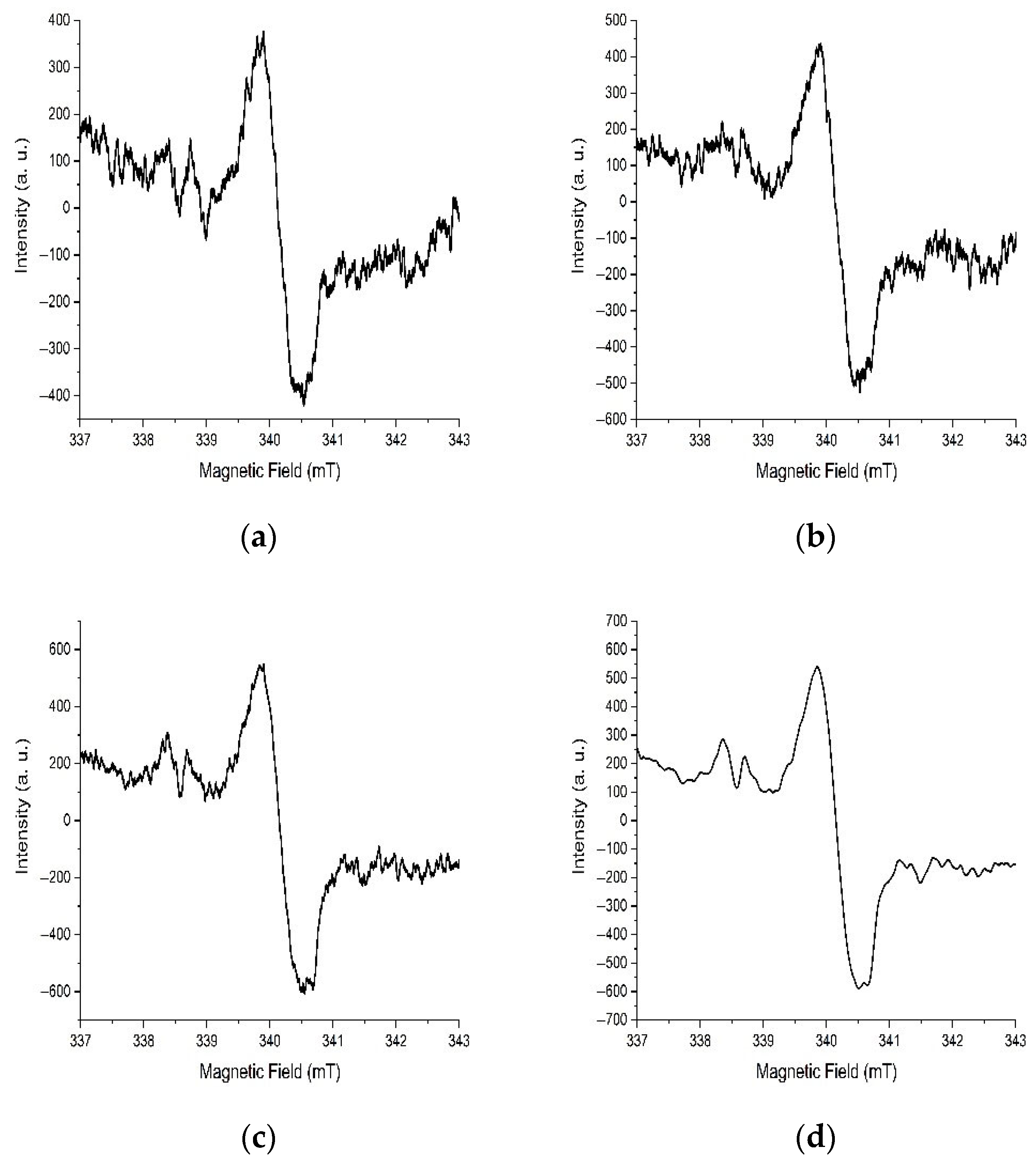
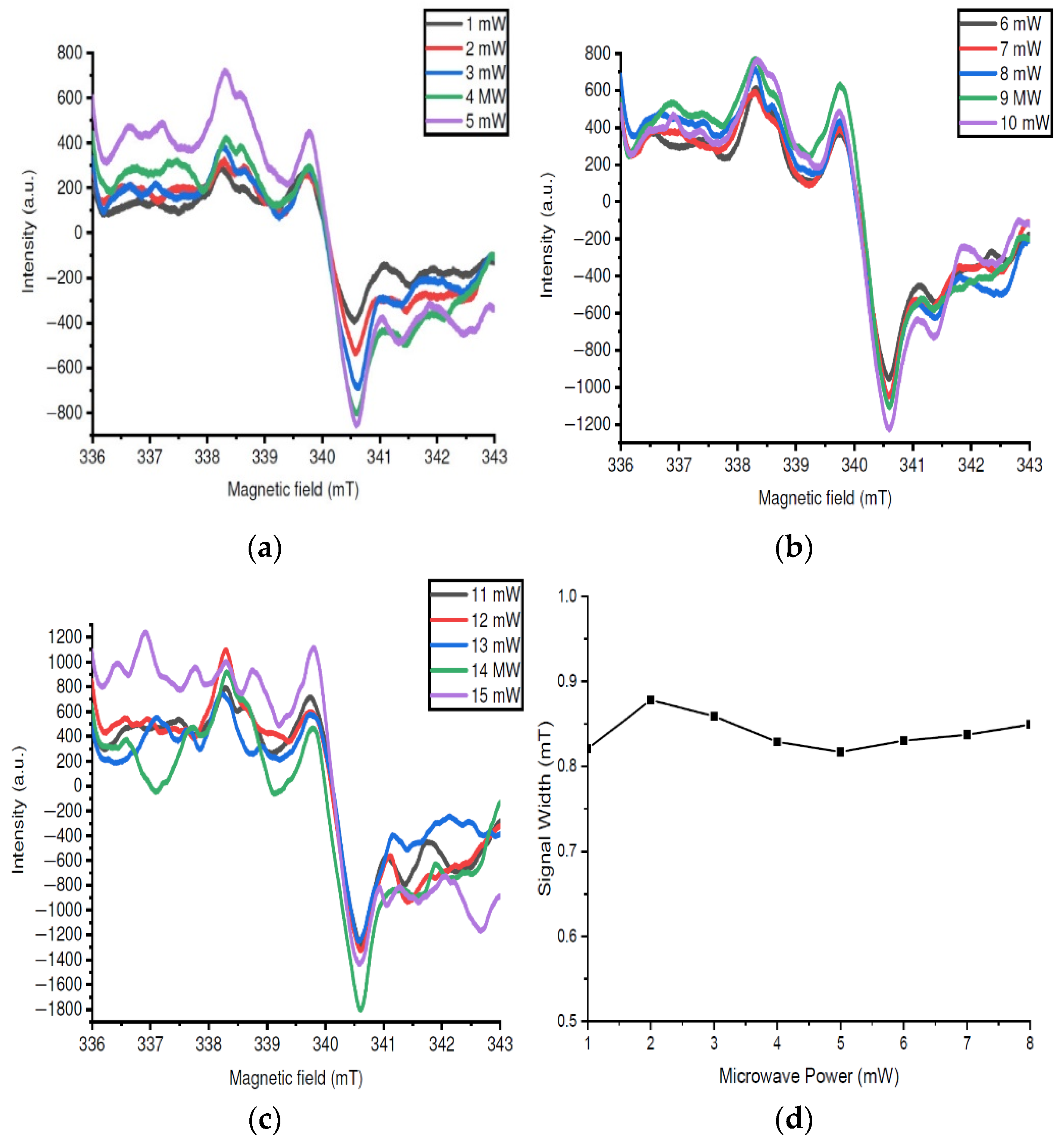
  • The stability of the EPR signal when subjected to a constant increase in microwave radiation power has shown a free energy exchange between homogeneous spins and the crystal lattice for structures with a high degree of organization under external excitation.
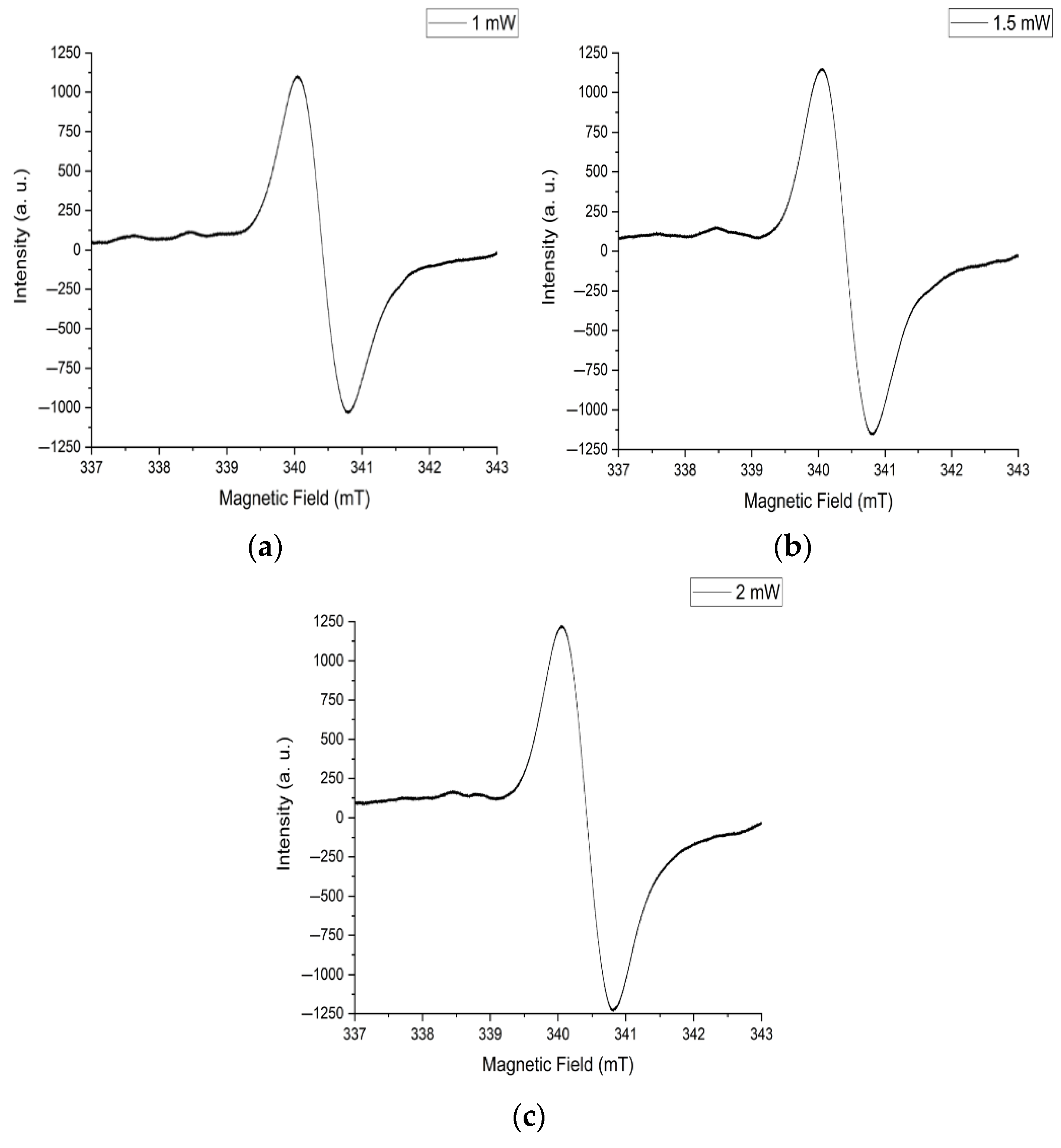
  • The isotropy of the properties of the PMCs responsible for the central EPR signal is due to the equally probable flow of charges in different directions along the axis of the nanowires.
This, as well as the donor nature of the particles responsible for the EPR signal, is the basis for the enhanced sensory properties of the material.
The application of a low-temperature method for producing ZnO/Por-Si nanostructures leads to a reduction in energy consumption.

2. Materials and Methods

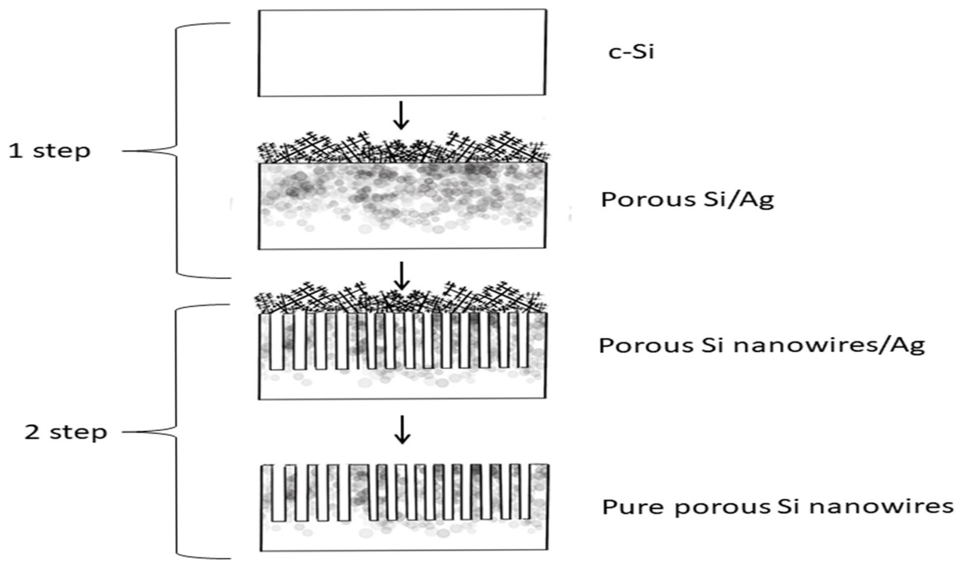
2.1. Synthesis and Transformation of the Studied Structures

The synthesis of porous silicon nanowires was carried by the method of two-stage modified metal-assisted electrochemical etching (MAECE) [17,18]. Synthesis was carried out in galvanostatic mode. In the first stage of electrochemical etching of a monocrystalline silicon substrate (p-Si (100), a specific resistance (12 Ohm*sm) was applied to form a composite of porous silicon and silver nanoparticles on its surface. The process took place in an aqueous alcohol solution of hydrogen fluoride (HF) and silver nitrate (AgNO3) at a concentration of 0.01 M. The duration of the process was 4.5 min, and the anodizing current density was 15 mA/cm2.
This method allowed for the deposition of silver nanoparticles on the surface of a porous matrix, without the penetration of silver into the depth of the porous layer. The use of silver is explained by its high catalytic activity. The electrolyte at the first stage contained the following components: water, alcohol, hydrofluoric acid, and AgNO3. Water is an oxidizing agent (oxidation of Si to SiO2), while hydrofluoric acid is an etching agent (etches SiO2). Alcohol allows for improving the wettability of the silicon wafer with electrolytes. AgNO3 serves as a source of silver.
At the second stage, the electrochemical etching of the obtained samples was performed in an aqueous alcohol solution of hydrofluoric acid (for 20 min at 180 mA/cm2) with the formation of wire structures. The silver deposited on the surface of the plate promoted the intensive local oxidation and subsequent spot etching of the oxidized area in hydrofluoric acid. Further, the samples were washed sequentially in an aqueous HNO3 solution, with isopropyl alcohol and distilled water. The following is a diagram of the formation of silicon nanowires (Figure 1).
The synthesis of ZnO was implemented in the following stages: At the first stage, the formation of the nucleus layer was carried out. For this purpose, 56 mg of zinc acetate ((CH3COO)2Zn) was dissolved in 50 mL of isopropyl alcohol. Then, the solution was deposited by centrifugation at 3000 rpm for 30 s on the porous surface. After that, the samples were dried at 150 °C for 5 min. To achieve a high concentration of ZnO nanoparticles in the pores of porous silicon nanowires (which are the growth centers of zinc oxide nanowires), the procedure was repeated 5 times. After that, the sample was annealed at 350 °C for 30 min.
At the second stage, the layer with wires was formed by a low-temperature hydro-thermal method. For this purpose, the following elements and quantities were used: zinc acetate (Zn(O2CCH3)2) = 175.6 mg, H2O = 80 mL, Hexamethylenetetramine = 112.1 mg, and STAV (Cetrimonium bromide) = 27.6 mg. The resulting solution was placed with a thermostat at and kept at 86 °C for 1 h. Further, the samples were annealed at 500 °C for 5 min.
The following is a balanced chemical reaction for the formation of ZnO:
Zn(O2CCH3)2 + (CH2)6N4 + 6H2O + C16H33N(CH3)3Br → ZnO↓
+ 2CH3COOH + 6HCHO + 4NH3 + C16H33N(CH3)3Br
The temperature treatment after the synthesis of the structures was carried out in an air atmosphere at 200 °C and 300 °C for 1 h. The choice of these temperatures was due to the following: Annealing in the range up to 400 degrees (200–300 °C) leads to an increase in the crystallinity of ZnO nanoparticles. In this case, there is a slight increase in the size of zinc oxide nanoparticles and crystallite grains.
On the contrary, higher annealing at 400 °C leads to an uneven redistribution of zinc particles, which can lead to the disruption of the structure of the substance and a decrease in crystallinity [19,20]. Based on this, temperatures of 200 and 300 °C were selected for annealing the structures.

2.2. Instrumentation

X-ray diffraction was used to study the structure of the surface layer of the samples. A highly collimated (0.05 × 1.5) mm2 monochromatic (CuKα) X-ray beam was focused at a 5° angle to the sample’s surface. The intensity of X-ray reflections along the diagram was measured every 2 = 0.05° using a microdensitometer (MD-100, Carl Zeu’s, Oberkochen, Germany). The Jones technique was used to determine the average size of the crystallites based on the half-widths of the X-ray lines.
Scanning electron microscopy (SEM): JSM-6490LA (“JEOL”, Akishima, Japan) was used to study the morphology of the surfaces of the structures. The take-off angle for the JSM-6490LA was 35°, and the analytical working distance was 10 mm. The microscope had a resolution of 3.0 nm. The elemental analysis of the samples was carried out using an analytical scanning electron microscope (JSM 6490 LA by JEOL) equipped with the JED 2300 EDS spectrometer (JEOL, Akishima, Japan).
The Gwiddion program, version 2.64 (Brno, Czech Republic) was applied to obtain three-dimensional microscopic images of surface structures and analyze the height distribution of structures.
Raman spectra for the analysis of nanowires structures was performed with a solver spectrum spectrometer Solver Spectrum (NT-MDT, Zelenograd, Russia).
Photoluminescence (PL) was recorded in the range of zinc oxide defects from 400 to 800 nm using a Cary Eclipse spectrophotometer (Agilent, Santa Clara, CA, USA). The spectral width of the slit in this device varied from 0.5 to 2.4 nm. A tungsten halogen lamp served as the radiation source for visible measurements.
The “JEOL” EPR spectrometer (JES-FA200, Akishima, Japan) can measure in the range between 9.4 GHz (X-Band) and 35 GHz (Q-Band). The microwave frequency stability was ~10−6. The sensitivity = 7 × 10⁹/10−4 T. The resolution was 2.35 μT. The output power ranges from 200 mW to 0.1 μW, with a quality factor (Q-factor) of 18,000.
Based on the presence of additional lines in the EPR spectrum, for their manifestation, it was necessary to choose the ratio between the scan time of the spectrum and the detector time constant. The most effective approach is to reduce the scan speed and time constant. Reducing the scanning speed, that is, increasing the spectrum scan time, ensures the detection of signals with low intensities. A decrease in the time constant also determines the detection of low-intensity signals that manifested in a short time. Therefore, the spectrum scan time was 2 min and the time constant was 0.1 s. To increase the signal-to-noise ratio by averaging the spectrum, the procedure was repeated 4 times.

3. Results

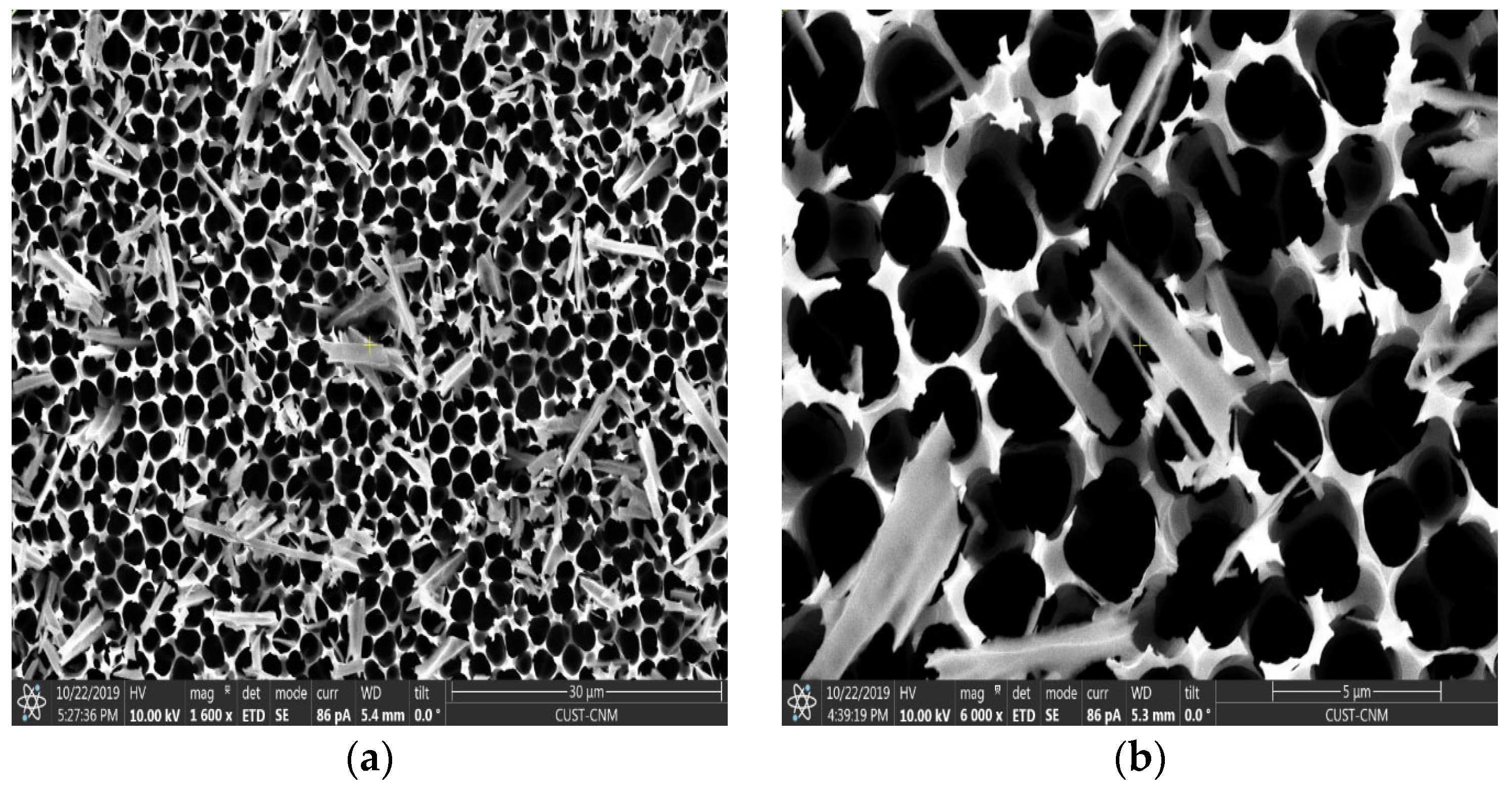
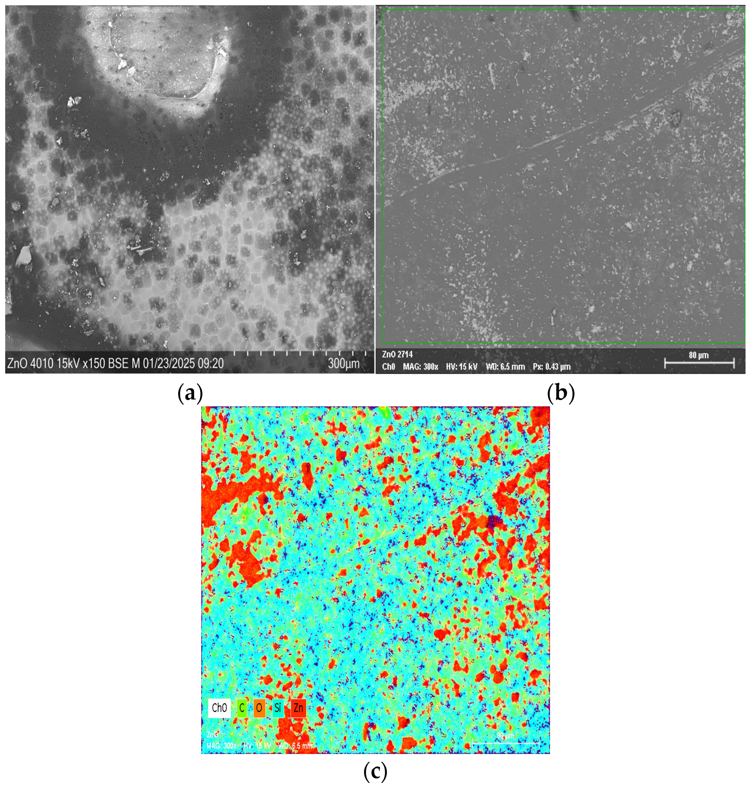
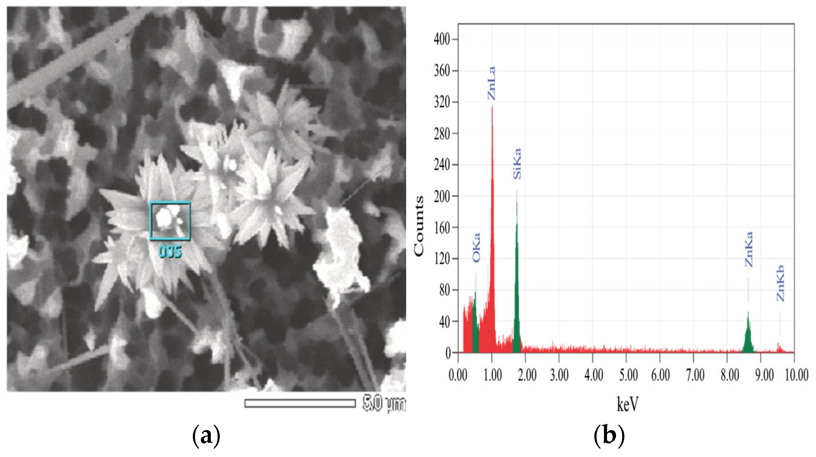
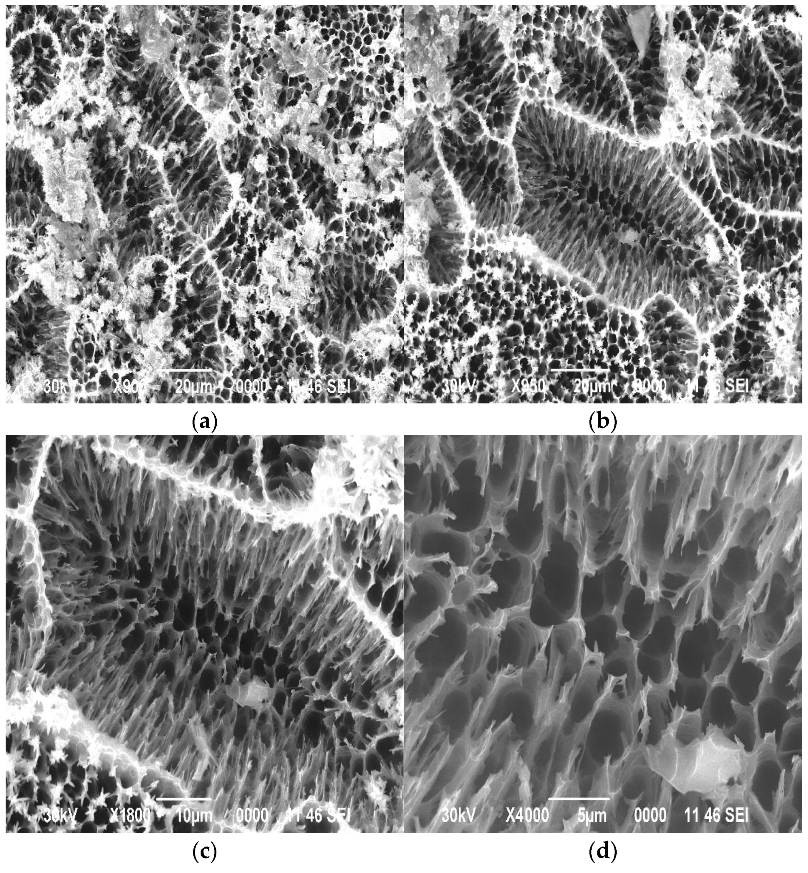
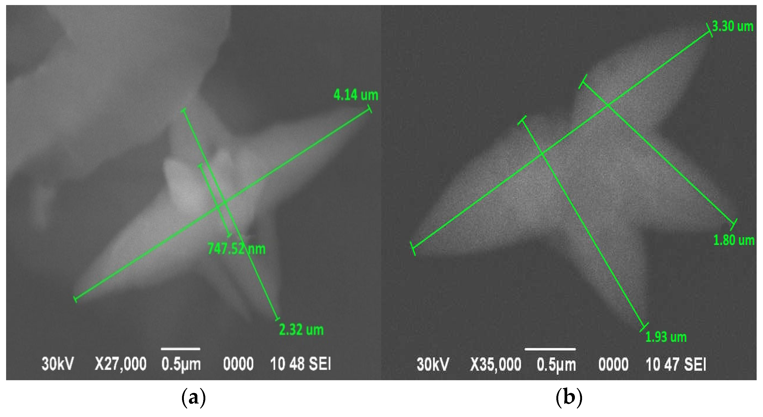
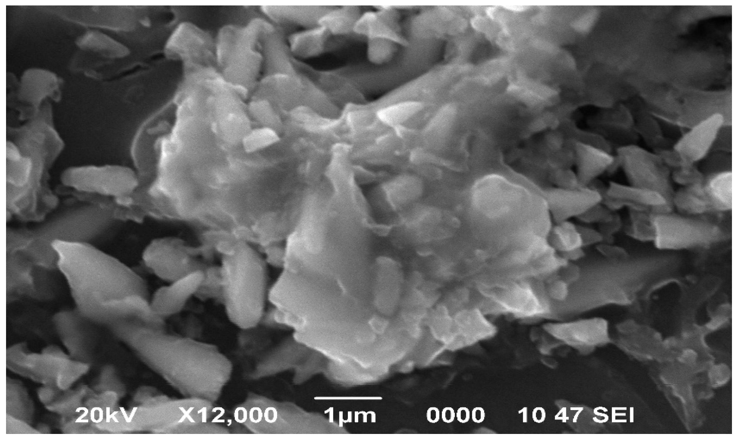
3.1. Study of Surface Morphology of Samples

The studies were carried out at all stages of the transformation of the surface structure. These included the formation of silicon nanowires, the synthesis of ZnO/PS structures, and samples after annealing 200 °C and 300 °C in an air atmosphere.
The surface of porous silicon after etching is a well-shaped structure, the boundaries of which consist of silicon nanowires connected by relatively thin walls (Figure 2). These structures are of great interest due to the high concentration of particles with broken bonds, which are potential growth centers for any surface formations.
SEM studies of the transverse cleavage of the samples showed a uniform nanowire structure (Figure 3). The directions of one-dimensional structures were predominantly vertical. The heights of the wires ranged from 2.58 microns to 4.22 microns. The average thickness was 292.6 nm.
Surface mapping was performed to determine the distribution of chemical elements after the deposition of zinc oxide on the porous surface. Silicon occupies the main part of the surface, but there were areas of significant accumulation of oxygen (Figure 4). The distribution of zinc corresponded to the same areas, which indicated the formation of zinc oxide particles on broken silicon bonds.
Elemental analysis showed the presence of a very small amount of zinc compared with other chemical elements (Figure 4, Table 1).
SEM images after ZnO deposition at high magnification allowed us to determine the formation of zinc oxide particles of three types: nanowires, flower-like structures, and clusters of matter (Figure 5, Figure 6 and Figure 7).
By applying the Gwiddion program, the height distribution of the structures was determined (Figure 5a). A three-dimensional model of the surface is shown in Figure 5b.
The clusters of matter were the highest structures. On the contrary, nanowires had a lower height.
Elemental analysis of flower-like crystallites showed a high concentration for zinc (Figure 6). The presence of silicon and oxygen was also determined (Table 2).
The following images show the ZnO/Por-Si sample surface containing structures of various levels, ranging from wires to clusters (Figure 7). The high level of development of the surface structure determines the increased sensory characteristics of the substance.
It is noticeable that flower-like structures were formed mainly on the tips of silicon nanowires and, in some places, on the bridges of the pore walls (Figure 8). In this case, zinc oxide nanowires were mainly formed along silicon nanowires (Figure 8).
The contents of wires with different linear sizes in flower-like structures are noticeable from Figure 9. More complex structures may contain several types of particles with an uncompensated charge.
The sample surface after ZnO deposition and annealing (t = 200 °C, 1 h, atmospheric air) consists of clusters of matter and flower-like and more complex structures (Figure 10). Nanowires are distinguishable in the cluster structure, whereas the components of the complex formation are fused wires and flower-like structures.
The main features of the surface of the samples after annealing were the less clear boundaries of wire-like and flower-like structures. This may be due to the nonequilibrium redistribution of zinc atoms in the structure of the sample. In areas of accumulation of various structures, the conditional coating density increased due to crystal accretion.
The annealing of 300 °C led to even greater changes. The boundaries of the crystallites became more blurred and a significant combination of flower-like structures, similar to melting, was noticeable (Figure 11). The thickness of the wires in the flower-like structures also increased.
Further enlargement of the structures led to an even greater increase in the zinc concentration in the surface layer of the sample (Figure 12, Table 3).

3.2. Investigation of the Sample Structure by XRD and Raman Spectroscopy Methods

Transformations of structures led to a change in the crystallinity level of the samples. X-ray diffraction studies have mainly shown the presence of a hexagonal structure of zinc oxide crystallites on the sample surface (Figure 13). Based on the contents of structures with different sizes on the surface, the variation in crystal sizes was different.
The presence of a Raman spectrum in the initial structures in this work indicates the formation of low-dimensional crystal structures (Figure 14). In this case, the photoluminescence signal appears after annealing due to the further process of the enlargement of the crystallized structures.
The presence of a high-intensity peak of about 540 cm−1 on Raman spectra is associated with the predominance of silicon in the structure of the initial samples (Figure 14). The small thickness of this peak is due to the high level of crystallinity of the structures as a result of repeated heat treatment.
A signal of about 450 cm−1 in Figure 14 indicates the presence of zinc oxide structures. The small width of this peak is noticeable in comparison with the peak at 540 cm−1. This is due to the presence of both crystalline and amorphous phases of ZnO. A significant difference in the intensity of these and silicon peaks indicates a low concentration of ZnO. The signal at 580 cm−1 is associated with a defective zinc oxide phase.

3.3. Photoluminescence Studies

The enlargement of crystals after annealing led to the appearance of photoluminescence. The decomposition of the PL spectrum into components indicates several reasons for the radiative recombination for these samples (Figure 15). The causes of photoluminescence are related to the defective structure of zinc oxide. Numerous researchers have observed the peak of the PL of the ZnO nanocrystalline phase at about 520 nm. Its origin is associated with the capture of charge by oxygen vacancies [22,23]. These particles and F-centers are charge donors. Charge transfer through vacancies is the main mechanism for determining the sensory characteristics of surface-active structures.

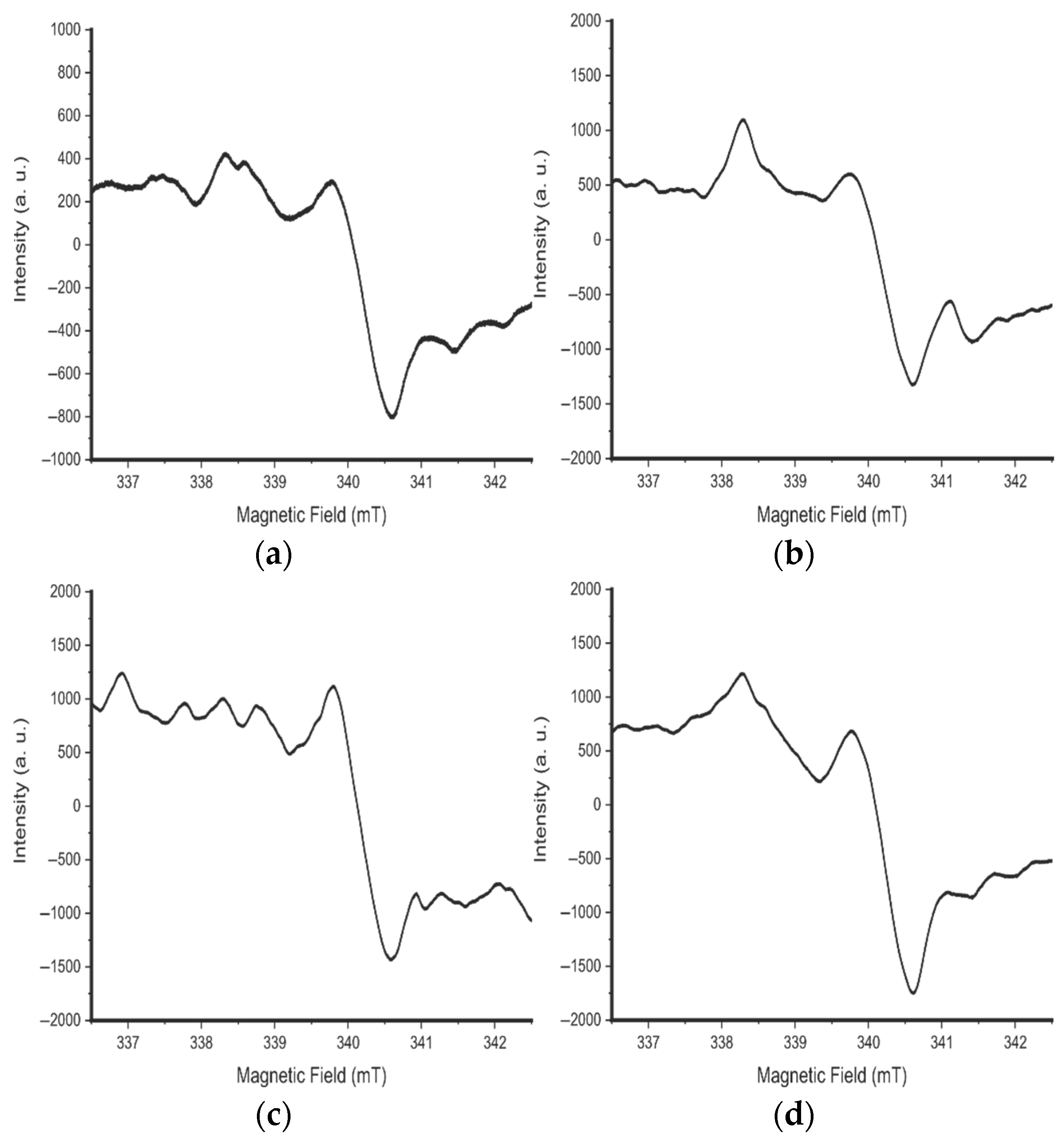
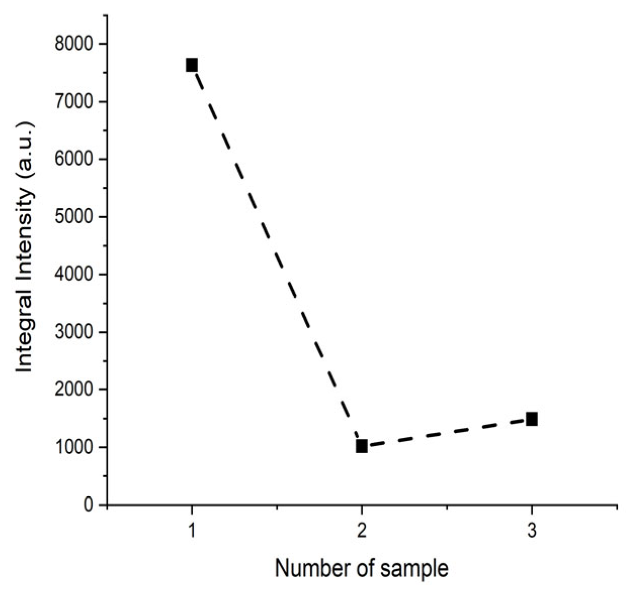
3.4. EPR Studies of Samples After Synthesis

The origin, formation, and transformation of structures are associated with defects in the crystal lattice. EPR spectroscopy was used for a detailed analysis in this area of research. The measurements took place with a sequential increase in microwave power. This was due to the manifestation of signals from different particles under varying measurement conditions. The general view of the spectrum is shown in the figures below (Figure 16).
There is a signal with a high intensity in the center of spectrum (Figure 16). The shape of this signal reflects the anisotropy of the local PM centers capable of trapping charges. Its origin, according to [9], is associated with charge donors. The signal shift to the region of lower magnetic field values is due to differences in the methods for obtaining samples. These particles are of great importance in the transfer of charges for sensors. However, Ref. [9] does not provide a more detailed analysis of this signal with the highest intensity in the spectrum.
The left part of the spectrum is associated with paramagnetic centers, which have different relaxation times (Figure 17). This is due to various changes in the signals with increasing microwave radiation power.
The subtraction of the spectra before annealing (Figure 18) shows the absence of saturation of the central signal with a sequential increase in microwave radiation power to 8 mW. This is manifested in a slight broadening of the spectrum. This is due to the continuous transition of charges from the ground energy state to the excited one. At the same time, the energy of excitation (absorption) and energy losses during relaxation are quite small. This is due to the free exchange of energy between homogeneous spins and the crystal lattice for structures with a high degree of organization.
The width of the signal is important in determining the characteristics of the PMC. This parameter for the signal in the center of the spectrum is less than 1 mT (Figure 19d). Therefore, this signal is narrow, involving few components (Figure 19a–c). Based on this, this signal is probably related to PMCs in the structure of ZnO nanowires.
When a potential difference is applied to the sample, charges flow from the silicon substrate (the bulk of the sample) into the nanowire, as this is an energetically advantageous path. The surface of the nanowires is formed mainly by vacancies of oxygen and zinc, which capture charges. In this case, vacancies exchange charges. This fast-moving process is due to the highly ordered structure of the nanowires. Thus, the width of the spectrum almost does not change.
Defects and their complexes have a spatial orientation. In this case, the direction of the external field affects their magnetic moments, which is reflected in the spectrum. EPR analysis of the central signal saturation in the initial state of the sample and after inversion shows the identity of the spectrum shape (Figure 20). This indicates the isotropic properties of PMCs. This is due to the equal probability of charges flowing in different directions along the axis of the nanowires.
The basis of the sensor’s response to external influences is the interaction with particles with an uncompensated charge (with broken bonds). The integral intensity of the spectrum (the area under the curve of the spectrum in integral form) is proportional to the concentration of paramagnetic centers in the sample. The concentration of PMC in the initial sample is highest based on the intensity of the central peak (Figure 21). This is due to the largest number of structures with a high specific surface area being present here. The transformation of structures after annealing leads to both decreases in the specific surface area and, accordingly, the concentration of PMCs (Figure 21).
The samples in these studies contain wire-shaped, flower-shaped, and more complex structures. The difference between them lies in the specific surface area and, accordingly, the concentration of particles with an uncompensated charge. This affects charge capture properties (the basis of sensory properties), as well as selectivity to external influences. Sensory properties are also related to the mechanism of charge transfer over vacancies. The highest concentration of vacancies is on the surface of structures. Thus, the samples containing mainly ZnO nanowires and flower-like structures (structures with the largest specific surface area) have the highest sensory properties. On the contrary, the formation of more complex structures leads to a decrease in the specific surface area and, consequently, sensory properties.

3.5. EPR Studies of Samples After Annealing at 200 °C

Heat treatment leads to a change in the structure and properties of paramagnetic centers. EPR studies after annealing (200 °C, air atmosphere, 1 h) resulted in a broadening of the central signal (Figure 22). At the same time, the signal intensity decreases.
Signal widening is associated with the unification of nanowires and the formation of more complex structures. The signal intensity decreased due to an increase in the number of interconnected structures.

3.6. EPR Studies of Samples After Annealing at 300 °C

The main feature of the EPR spectrum for the sample after annealing at 300 °C is the symmetry and isotropy of the central signal (Figure 23). There is also a greater increase in signal intensity than after annealing at 200 °C. The distribution of paramagnetic centers in the sample volume is uniform based on the isotropy of the central signal.

4. Conclusions

The surface structure of the samples, consisting of silicon nanowires, was formed using a modified MAESE method. As a result of zinc oxide deposition on a porous surface at the ends of silicon nanowires, a set of structures with different dimensions was synthesized. The samples before annealing had pronounced Raman spectra from the ZnO and Si structures. The annealing of the samples at 200 °C in air atmosphere led to the enlargement of the crystallites. Studies of photoluminescence in the defective region of the ZnO spectrum after annealing samples have shown the presence of several causes of radiation recombination. EPR studies of samples after ZnO formation showed the presence of a narrow-width signal. This spectrum did not change shape with a sequential increase in microwave power. This indicates the probability of the almost free transfer of charges through the formed structures. Annealing at 200 °C in air atmosphere led to a broadening of the EPR spectrum and a decrease in signal intensity. Heat treatment at 300 °C increased the intensity of the EPR spectrum. This increased the likelihood of charges being captured and transferred by particles with broken bonds under the influence of an external field.

Author Contributions

Conceptualization, V.M. and D.M.; methodology, A.G.; software, A.K.; validation, E.A.D. and M.B.; formal analysis, T.S.; investigation, R.Z.; resources, A.G.; data curation, A.K. and P.O.; writing—original draft preparation, D.M.; writing—review and editing, R.Z.; visualization, M.B. and P.O.; supervision, V.M.; project administration, E.A.D.; funding acquisition, Y.S. All authors have read and agreed to the published version of the manuscript.

Funding

This research was funded by the Science Committee of the Ministry of Science and Higher Education of the Republic of Kazakhstan (Grant No. BR21881954 “Development of technologies for the synthesis of nanostructured materials for efficient photocatalytic electrodes, photo- and gas-sensors”).

Data Availability Statement

The original contributions presented in this study are included in the article. Further inquiries can be directed to the corresponding author.

Conflicts of Interest

The authors declare no conflicts of interest.

References

  1. Begunov, M.; Gagarina, A.; Zhapakov, R.; Murzalinov, D.; Seredavina, T.; Novikova, K.; Kemelbekova, A.; Spivak, Y.; Moshnikov, V.; Dmitriyeva, E. An Investigation of the Synthesis of a Hybrid Homogeneous Structure of ZnO/Si Nanowires with Stable Energy Properties. Eng. Proc. 2024, 67, 28. [Google Scholar] [CrossRef]
  2. Hsu, C.-Y.; Rheima, A.; Abbas, Z.; Faryad, M.; Kadhim, M.; Altimari, U.; Dawood, A.; Al-Bayati, A.; Abed, Z.; Radhi, R.; et al. Nanowires Properties and Applications: A Review Study. S. Afr. J. Chem. Eng. 2023, 46, 286–311. [Google Scholar] [CrossRef]
  3. Abdulgafour, H.I.; Hassan, Z.; Yam, F.K.; Jawad, M.J. Growth of ZnO nanowires without catalyst on porous silicon. AIP Conf. Proc. 2011, 1341, 18–20. [Google Scholar] [CrossRef]
  4. Sherstnev, A.I.; Chubenko, E.B.; Redko, S.V.; Petrovich, V.A.; Pilipenko, V.A.; Bondarenko, V.P. Formation of nanocomposite materials based on porous silicon and zinc oxide by electrochemical method. Rep. Belarusian State Univ. Inform. Radioelectron. 2016, 95, 82–88. [Google Scholar]
  5. Stehr, J.E.; Chen, S.L.; Chen, W.M.; Cai, L.; Shen, S.; Buyanova, I.A. Identification of a Nitrogen-related acceptor in ZnO nanowires. Nanoscale 2019, 11, 10921–10926. [Google Scholar] [CrossRef]
  6. Dey, S.; Mohanty, D.; Divya, N.; Bakshi, V.; Mohanty, A.; Rath, D.; Das, S.; Mondal, A.; Roy, S.; Sabui, R. A Critical Review on Zinc Oxide Nanoparticles: Synthesis, Properties and Biomedical Applications. Intell. Pharm. 2024, 3, 53–70. [Google Scholar] [CrossRef]
  7. Schwan, A.M.; Chwatal, S.; Hendler, C.; Kopp, D.; Lackner, J.M.; Kaindl, R.; Tscherner, M.; Zirkl, M.; Angerer, P.; Friessnegger, B.; et al. Morphology-controlled atmospheric pressure plasma synthesis of zinc oxide nanoparticles for piezoelectric sensors. Appl. Nanosci. 2023, 13, 6421–6432. [Google Scholar] [CrossRef]
  8. Erdem, E.; Justeau, C.; Poulin-Vittrant, G. Investigation of Intrinsic and Extrinsic Defect Centers of ZnO Nanowires for Nano-Generators. LE Stud. Multidiscip. J. 2018, 61–64. [Google Scholar] [CrossRef]
  9. Stehr, J.E.; Chen, W.M.; Reddy, N.K.; Tu, C.W.; Buyanova, I.A. Efficient nitrogen incorporation in ZnO nanowires. Sci. Rep. 2015, 5, 13406. [Google Scholar] [CrossRef]
  10. Hsu, H.C.; Cheng, C.S.; Chang, C.C.; Yang, S.; Chang, C.S.; Hsieh, W.F. Orientation-enhanced growth and optical properties of ZnO nanowires grown on porous silicon substrates. Nanotechnology 2005, 16, 297. [Google Scholar] [CrossRef]
  11. Ryabko, A.A.; Nalimova, S.S.; Permyakov, N.V.; Bobkov, A.A.; Maksimov, A.I.; Kondratev, V.M.; Kotlyar, K.P.; Ovezov, M.K.; Komolov, A.S.; Lazneva, E.F.; et al. Architectonics of Zinc Oxide Nanorod Coatings for Adsorption Gas Sensors. Tech. Phys. 2024, 69, 2103–2110. [Google Scholar] [CrossRef]
  12. Yang, J.J.; Pickett, M.D.; Li, X.; Ohlberg, D.A.; Stewart, D.R.; Williams, R.S. Memristive switching mechanism for metal/oxide/metal nanodevices. Nat. Nanotechnol. 2008, 3, 429–433. [Google Scholar] [CrossRef] [PubMed]
  13. Sawa, A. Resistive switching in transition metal oxides. Mater. Today 2008, 11, 28–36. [Google Scholar] [CrossRef]
  14. Zoolfakar, A.S.; Kadir, R.A.; Rani, R.A.; Balendhran, S.; Liu, X.; Kats, E.; Bhargava, S.K.; Bhaskaran, M.; Sriram, S.; Zhuiykov, S.; et al. Engineering electrodeposited ZnO films and their memristive switching performance. Phys. Chem. Chem. Phys. 2013, 15, 10376–10384. [Google Scholar] [CrossRef]
  15. Liu, L.; Chen, B.; Gao, B.; Zhang, F.; Chen, Y.; Liu, X.; Kang, J. Engineering oxide resistive switching materials for memristive device application. Appl. Phys. A 2011, 102, 991–996. [Google Scholar] [CrossRef]
  16. Martínez, L.; Ocampo, O.; Kumar, Y.; Agarwal, V. ZnO-porous silicon nanocomposite for possible memristive device fabrication. Nanoscale Res. Lett. 2014, 9, 437. [Google Scholar] [CrossRef]
  17. Gagarina, A.Y.; Bogoslovskaya, L.S.; Spivak, Y.M.; Novikova, K.N.; Kuznetsov, A.; Moshnikov, V.A. Synthesis of arrays nanostructured porous silicon wires in electron conductivity type silicon with crystallographic orientation (111). Tech. Phys. 2023, 68, 254. [Google Scholar] [CrossRef]
  18. Sekar, K.; Doineau, R.; Mayarambakam, S.; Schmaltz, B.; Poulin-Vittrant, G. Control of ZnO nanowires growth in flexible perovskite solar cells: A mini-review. Heliyon 2014, 10, e24706. [Google Scholar] [CrossRef]
  19. Alshoaibi, A. The Influence of Annealing Temperature on the Microstructure and Electrical Properties of Sputtered ZnO Thin Films. Inorganics 2024, 12, 236. [Google Scholar] [CrossRef]
  20. Uthirakumar, P.; Hong, C.-H. Effect of annealing temperature and pH on morphology and optical property of highly dispersible ZnO nanoparticles. Mater. Charact. 2009, 60, 1305–1310. [Google Scholar] [CrossRef]
  21. Murzalinov, D.; Zhapakov, R. The evolution of defect formation during the deposition of thin layers of ZnO on the surface of hierarchical porous silicon and subsequent multi-stage annealing. In Proceedings of the 3rd International Electronic Conference on Processes, Virtual, 29–31 May 2024; MDPI: Basel, Switzerland, 2024. [Google Scholar]
  22. Murzalinov, D.; Seredavina, T.; Kemelbekova, A.; Spivak, Y.; Moshnikov, V.; Mukhamedshina, D.; Fedosimova, A. Investigation of Surface Nanoclusters and Paramagnetic Centers of ZnO/Por-Si Structures as the Basis of Sensory Properties. Processes 2023, 11, 3332. [Google Scholar] [CrossRef]
  23. Rodnyi, P.A.; Chernenko, K.A.; Venevtsev, I.D. Mechanisms of ZnO Luminescence in the Visible Spectral Region. Opt. Spectrosc. 2018, 125, 372–378. [Google Scholar] [CrossRef]
Figure 1. A diagram of the stages of the formation of silicon nanowires.
Processes 13 02099 g001
Figure 2. SEM images of the silicon surface after etching: (a) resolution: 30 µm; (b) resolution: 5 µm.
Processes 13 02099 g002
Figure 3. SEM images of the nanowire structures of the samples before zinc oxide deposition, with magnification of (a) 2 microns and (b) 4 microns.
Processes 13 02099 g003
Figure 4. The surface mapping of ZnO/Por-Si structures obtained by the SEM method: (a) an SEM image with a resolution of 300 µm; (b) an SEM image with a resolution of 80 µm; (c) surface mapping.
Processes 13 02099 g004
Figure 5. (a) An analysis of the height distribution of surface structures for the ZnO/Por-Si sample; (b) a three-dimensional model of surface structures for the ZnO/Por-Si sample.
Processes 13 02099 g005
Figure 6. The elemental analysis of flower-like structures: (a) an SEM image of a flower-like structure; (b) an elemental analysis of ZnO/Por-Si sample flower-like structures.
Processes 13 02099 g006
Figure 7. SEM images of the surface structure of the initial sample, combining particles with different dimensions [21]: (a)—900× magnification; (b)—950× magnification; (c)—1800× magnification; (d)—4000× magnification.
Processes 13 02099 g007
Figure 8. SEM images of flower-like structures formed at the boundaries of pores [21]: (a)—6000× magnification; (b)—10,000× magnification; (c)—12,000× magnification; (d)—3300× magnification.
Processes 13 02099 g008
Figure 9. SEM images of flower-like structures: (a)—27,000× magnification; (b)—35,000× magnification.
Processes 13 02099 g009
Figure 10. SEM image of the surface of the samples after annealing: (a)—10,000× magnification; (b)—14,000× magnification.
Processes 13 02099 g010
Figure 11. SEM images of the sample after annealing at 300 °C: (a) 3500× magnification; (b) 12,000× magnification.
Processes 13 02099 g011
Figure 12. SEM image of clusters of matter after annealing samples at 300 °C.
Processes 13 02099 g012
Figure 13. XRD spectra of samples after annealing at 200 °C in an air atmosphere.
Processes 13 02099 g013
Figure 14. The Raman spectrum of the initial samples.
Processes 13 02099 g014
Figure 15. The photoluminescence spectra of samples after annealing at 200 °C in an air atmosphere (The red line is the PL spectrum for a sample after annealing, the green lines are the decomposition of the spectrum into Gaussians).
Processes 13 02099 g015
Figure 16. The EPR spectra of the initial samples: (a) spectrum scan time—2 min, repetition—2 times, time constant—0.1 s, signal gain—800; (b) spectrum scan time—2 min, repetition—2 times, time constant—0.1 s, signal gain—1000; (c) spectrum scan time—2 min, repetition—2 times, time constant—0.1 s, signal gain—1200; (d) spectrum scan time—2 min, repetition—4 times, time constant—0.1 s, signal gain—1200.
Processes 13 02099 g016
Figure 17. The EPR spectra of the initial sample at microwave power: (a) 4 mW, (b) 12 mW, (c) 15 mW, and (d) 18.7 mW.
Processes 13 02099 g017
Figure 18. The subtraction of the EPR spectra of the initial sample at microwave power of 6 mW and 1.5 mW (The black line is the spectrum at a microwave power of 6 mW, the red line is the spectrum at a microwave power of 1.5 mW, the green line is the result of subtracting the spectra).
Processes 13 02099 g018
Figure 19. EPR spectra of the initial sample with increasing microwave power: (a) from 1 mW to 5 mW; (b) from 6 mW to 10 mW; (c) from 11 mW to 15 mW; (d) the dependence of the signal width on the increase in microwave power.
Processes 13 02099 g019
Figure 20. EPR spectra of the initial sample with a sequential increase in microwave power: (a) from 1.2 to 2.4 mW, initial position of the sample; (b) from 1.2 to 2.4 mW, sample inverted; (c) from 2.8 to 4 mW, initial position of the sample; (d) from 2.8 to 4 mW, sample inverted.
Processes 13 02099 g020
Figure 21. The dependence of the integral intensity of the central EPR signal on the heat treatment temperature: 1—the initial sample; 2—the sample after annealing at 200 °C; 3—the sample after annealing at 300 °C.
Processes 13 02099 g021
Figure 22. EPR spectra of annealed samples at microwave power: (a) 4 mW, (b) 6.2 mW, (c) 7.8 mW, and (d) 11 mW.
Processes 13 02099 g022
Figure 23. EPR spectra of annealed samples at 300 °C with microwave power of (a) 1 mW, (b) 1.5 mW, and (c) 2mW.
Processes 13 02099 g023
Table 1. Elemental analysis of the near-surface zone of ZnO/Por-Si structures.
ElementAt. No.NettoMass [%]Mass Norm. [%]Atom [%]Abs. Error [%] (1 sigma)Rel. Error [%] (1 sigma)
C645,51826.8726.8745.681.485.51
O832,3456.246.247.960.345.45
Si142,539,35561.4561.4544.671.702.77
Zn3014,2435.445.441.700.162.96
Sum 100.00100.00100.00
Table 2. The results of the elemental analysis of flower-like structures.
Element(kEV)Mass%Error%At%K
O K0.5252.480.137.772.7645
Si K1.73917.100.1830.5312.0252
Zn K8.63080.422.4561.7085.2104
Total 100.00 100.00
Table 3. The results of the elemental analysis of flower-like structures after the annealing of samples at 300 °C (Fitting Coefficient: 0.3893).
Element(kEV)Mass%Error%At%K
O K-----
Si K1.7399.410.2919.484.7032
Zn K8.63090.591.2680.5295.2968
Total 100.00 100.00
Disclaimer/Publisher’s Note: The statements, opinions and data contained in all publications are solely those of the individual author(s) and contributor(s) and not of MDPI and/or the editor(s). MDPI and/or the editor(s) disclaim responsibility for any injury to people or property resulting from any ideas, methods, instructions or products referred to in the content.

