1. Introduction
After the recent Fukushima accident, the dangers of nuclear power plants became directly exposed to the public [
1]. Therefore, not only nuclear power plant workers but also the general public should always carry a radiation detector that can protect their own lives and safety to cope with the threat of nuclear power plant accidents [
2].
The system in
Figure 1 is a portable radiation detection system that can be installed on a smartphone and can be easily carried and used by ordinary people. Since this special-purpose small embedded system can utilize the smartphone’s battery and mobile application processor (AP), it has the advantage of being able to build a radiation detection system by implementing only a few simple circuits. Therefore, the mobile radiation dosimeter system in
Figure 1 can be composed of only three sub-blocks: a radiation detector, a sensor interface circuit, and a power conversion circuit. First, the radiation detector is responsible for converting the input radiation particles into a charge signal (
ISiPM). A silicon photomultiplier (SiPM), a type of radiation detector, can be manufactured by using the semiconductor process and has a high density of integration even with a small area, so it is suitable for mobile applications. In an SiPM, radiation particles injected into the SiPM composed of a scintillator and a reverse-biased photodiode are converted to light energy through the scintillator. Finally, the SiPM can generate a charge signal proportional to the energy of the radiation particles. Second, the charge-sensitive amplifier (CSA) in the sensor interface circuits amplifies the charge signal delivered from the SiPM through the sensing resistor (
Rs) and capacitor (
Cs). Additionally, the analog-to-digital converter (ADC) converts the buffered voltage signal into a digital signal that can be processed by the back-end system built into the smartphone. Third, the power management circuits serve to drive the voltages required for the radiation detector (HVDD) and sensor interface circuits (AVDD, DVDD) from the smartphone battery.
Radiation detection systems manufactured in previous studies with SiPM boast a high performance but have a fatal drawback of low portability [
3,
4]. This is because SiPM-based high-performance radiation detectors require a high driving voltage. Therefore, if a power conversion circuit optimized for the charge generation characteristics of the SiPM is applied, the portability of the radiation detection system may be increased. However, an SiPM has problems that are difficult to optimize with the conventional power conversion circuits due to its unique electrical characteristics. First, according to the commercial product [
5], a driving voltage of more than 25.5 V is required. In other words, it can be seen that a step-up DC–DC converter should be designed to receive the voltage of a Li-ion battery (3.7 V) and generate a high voltage that is nearly eight times higher. Second, as shown in
Figure 2, it shows a low power characteristic of at least 1 mA in normal mode. However, when radiation particles are injected, a maximum current of 20 mA can flow for several hundred ns. Therefore, the step-up converter for the SiPM should be able to achieve high efficiency by ensuring optimized operation for the current characteristics in
Figure 2.
In general, a step-up DC–DC converter can be implemented with the topology of an SC (Switched Capacitor)-based charge pump or an SI (Switched Inductor)-based boost converter [
6,
7] as shown in
Figure 3. First, the charge pump has the advantage of being able to achieve a high conversion ratio with a relatively simple method by connecting several capacitor (
CN) and diode (
DN) stages in series, but it is difficult to achieve a high conversion ratio under load conditions of several tens of mW or more. Otherwise, there may be disadvantages of lowering the efficiency. Second, the boost converter shows high efficiency even under a load condition of several hundred mW or more. It consists of an inductor (
L), diode (
D), and a switch controlled by a pulse width modulator. However, it has a disadvantage because it is difficult to expect a fast transient response in a low-power application. In this work, a boost converter was selected to achieve a high conversion ratio. In addition, a circuit for operation optimized for the current characteristics of SiPM was proposed to achieve fast transient response characteristics.
This paper is organized in the following order. First, in
Section 1, the necessity of the portable radiation detection system developed in this study is discussed. Second, in
Section 2, the key concept of the boost converter proposed in this study is explained. Third, in
Section 3, the circuit implementation of the proposed boost converter is described. Finally,
Section 4 and
Section 5 will discuss the simulation results and the conclusions of this study, respectively.
2. Key Concept of Proposed Boost Converter
As described above, a switched inductor-based boost converter was selected as the basic topology for driving the SiPM.
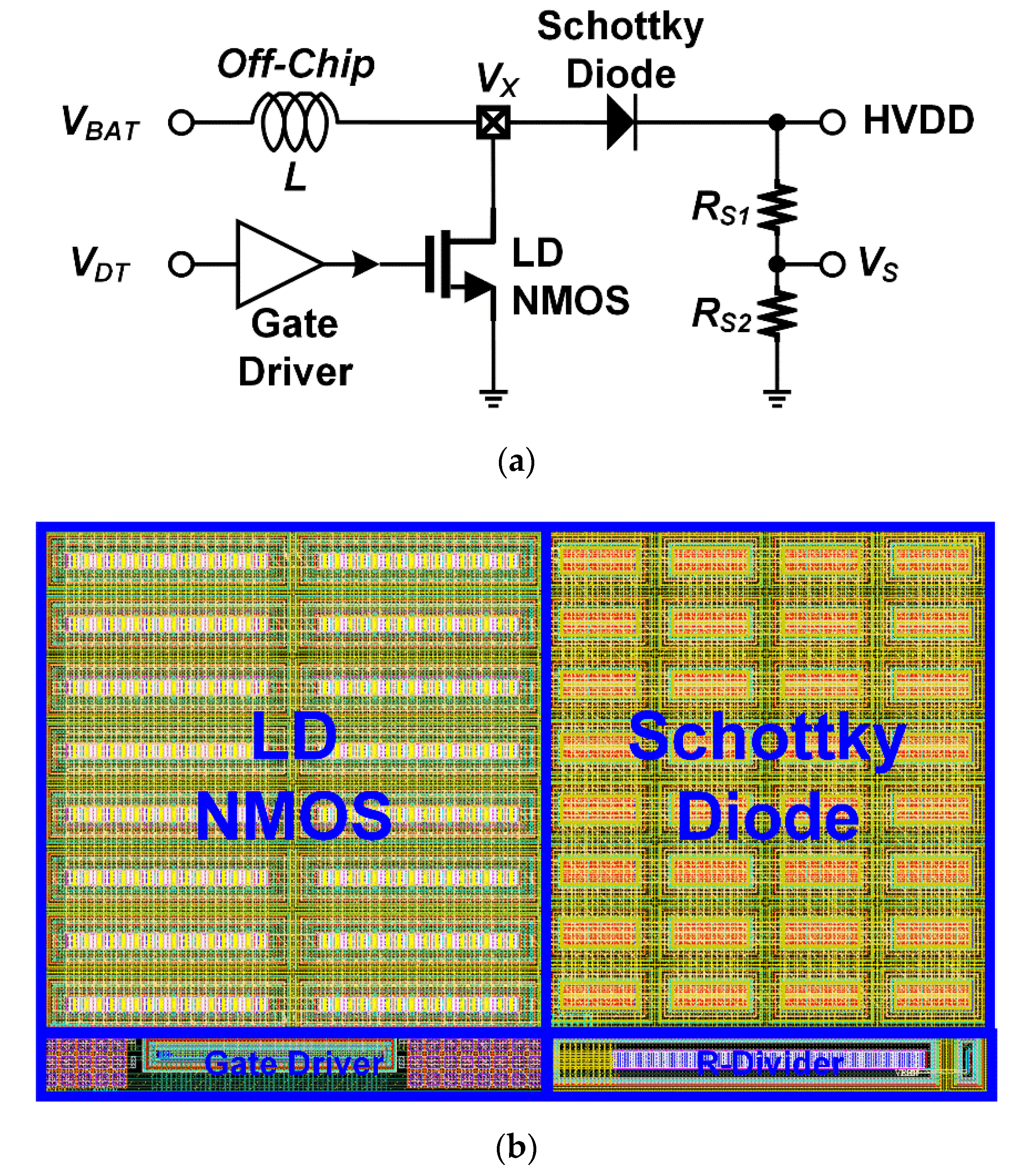
Figure 4a shows the basic configuration of a voltage-mode boost converter to generate a voltage from 3.7 to 25.5 V. First, the power stage composed of an inductor (
L), a Schottky diode (
D), and switch plays a role in generating output voltage by pulse width modulation (PWM) signal. Considering that the output voltage is 25.5 V and is controlled in discrete continuous mode (DCM), it is composed of an asynchronous-type topology that freewheels the build-up current with a Schottky diode. Second, the PWM controller, which consists of a voltage divider (
RS1,
RS2), loop filters (
Gm,
RZ,
CI), and comparator, can generate a duty signal (
VDT) proportional to the output voltage drop. When radiation particles enter the SiPM, a radiation-induced charge is generated. Additionally, a voltage drop proportional to the amount of charge is generated at the output stage. The voltage divider scales down the voltage drop at the output, and the compensator implemented as a Gm-C loop filter integrates this error voltage (
VE). Additionally, the comparator generates
VDT by comparing
VE and sawtooth waveform. Finally, the
VDT controls the switch of the power stage to fill the voltage drop of the output stage.
Figure 4b shows a small signal model of a voltage-mode boost converter. In DCM, there is one pole (
ωp,p) in the power stage, and the poles (
ωp,G) and zeros (
ωz,G) of the loop filters determine the loop stability.
The basic configuration of the boost converter to be implemented in this study was designed to be in voltage mode, not current mode. This is because the current sensing circuit for realizing the current mode consumes relatively high power [
8], so there is a risk of greatly reducing the efficiency of the boost converter. However, a voltage-mode-based boost converter has too narrow a loop bandwidth, so it is difficult to guarantee the fast recovery speed. In the case of the SiPM, after one radiation event occurs, it should be possible to recover the basic driving voltage of the SiPM before a new event to be input occurs. Therefore, the boost converter of voltage mode for SiPM needs to compensate for the disadvantage of not implementing current mode.
In order to compensate for the slow transient characteristics of the voltage-mode based boost converter, circuit techniques that are not normally used are suggested. First, a method was used to increase the low-frequency pole generated in the power stage to a high frequency by using a load capacitor that is close to 1000 times smaller (
Figure 5). Of course, since the ripple increases when the load capacitor is reduced, it is a method that general DC–DC converters do not use. Fortunately, as long as the SiPM can only sustain more than the voltage required by the datasheet, the ripple characteristic is not very important. Second, a method to further increase the loop bandwidth only at the moment of load transient is proposed, going beyond the method of reducing
CLoad. If the conventional sawtooth waveform (CST) is changed to a quadratic sawtooth waveform (QST), as shown in the circuit diagram in
Figure 6a, the changed pulse width of the
VDT (
Dt1 to
Dt2) can be made much larger, even with the same error voltage change (
VE1 to
VE2). This is because CST generates a change in
VDT that is proportional to the only amount of change in the error voltage, but QST can generate a change in the duty signal that corresponds to the square of the amount of change in the error voltage. As a result, it is possible to show much faster transient characteristics than in the conventional boost converter using CST. Compared to
Figure 4b, the gain of the PWM generator in
Figure 6b is increased by about 1.4 times. In other words, the boost converter can achieve the effect of increasing the loop bandwidth by 1.4 times by applying the QST circuits.
3. Detailed Implementations of Proposed Boost Converter
In this section, the implementation of the concept proposed in
Section 3 is discussed. To verify the performance of the circuit proposed in this study, a PDK (Process Design Kit) of 0.18 um BCD process was used.
The power stage was composed of an inductor, a power switch, and a diode, as shown in
Figure 7a. The inductor was modeled with 10 µH and DCR 700 mOhm, which are pure inductance values, and the parasitic capacitance considered in the actual inductor pad was 10 pF. Since the
Vx node switches from ground to 27 V according to the operation of the power stage, n-type LDMOS (laterally diffused metal-oxide semiconductor) and Schottky diodes, each with a tolerance of up to 35 V, were used. The power switch was optimized and designed based on the averaged load current of 2 mA, and the inverter chain-based gate driver was designed to be fully turned on and off.
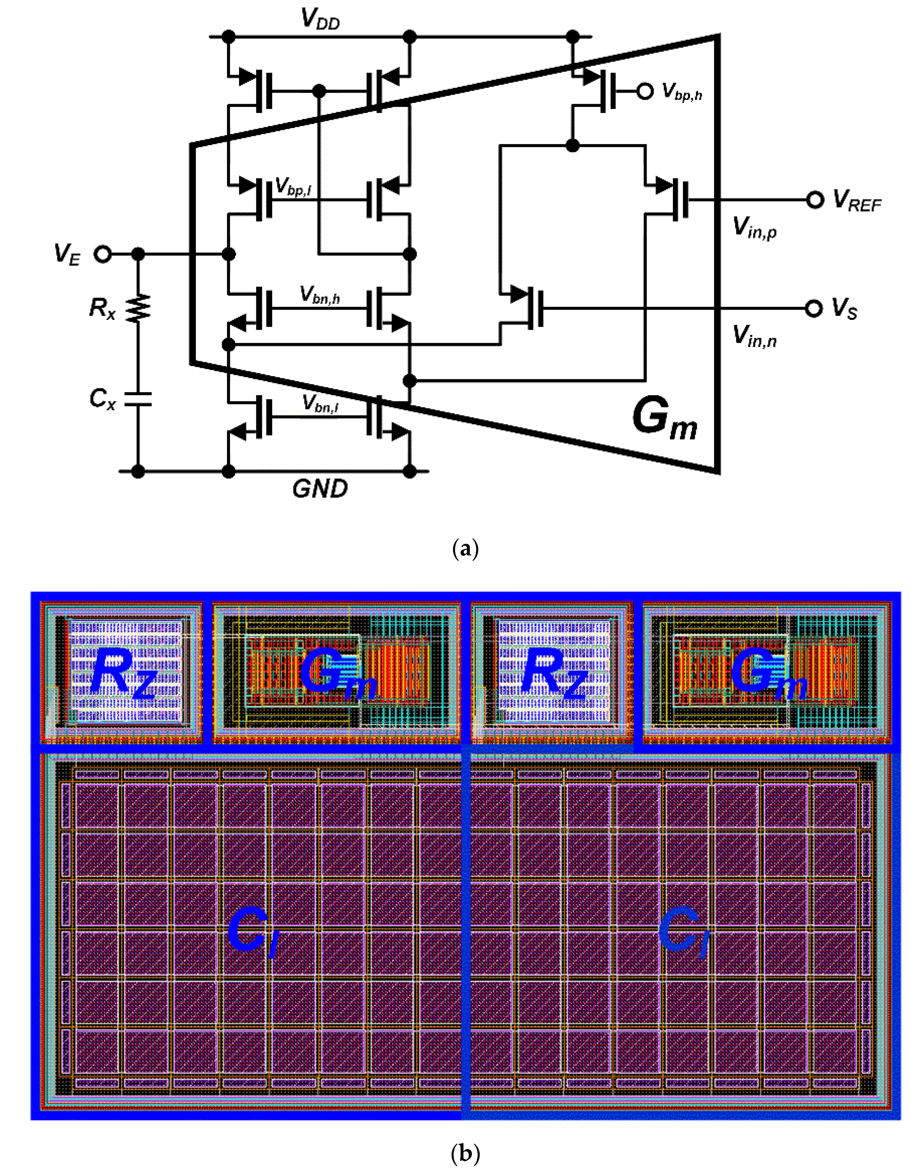
Figure 8 shows the loop filters that create an error voltage. The loop filter used in this study was made based on the folded cascode OTA, and two OTAs were cascaded to prevent the loop gain from being reduced by the voltage divider. In addition, a capacitor (
Cx) calculated as a pole was connected to the output along with the transconductance value of OTA, and the resistor (
Rz) inserted in series with this has the effect of inserting zero together with
Cx. The power consumption of each OTA is 4 μW, and it is designed in an edge that does not reduce conversion efficiency.
The newly proposed PWM generator in this study was designed as shown in
Figure 9. By using the CST generation circuit to convert the sawtooth-type voltage signal into a current and integrate it back into the capacitor, the square characteristic could be obtained with respect to time. The power used in the circuit of
Figure 9 could be designed with a negligible level of 4 μW.
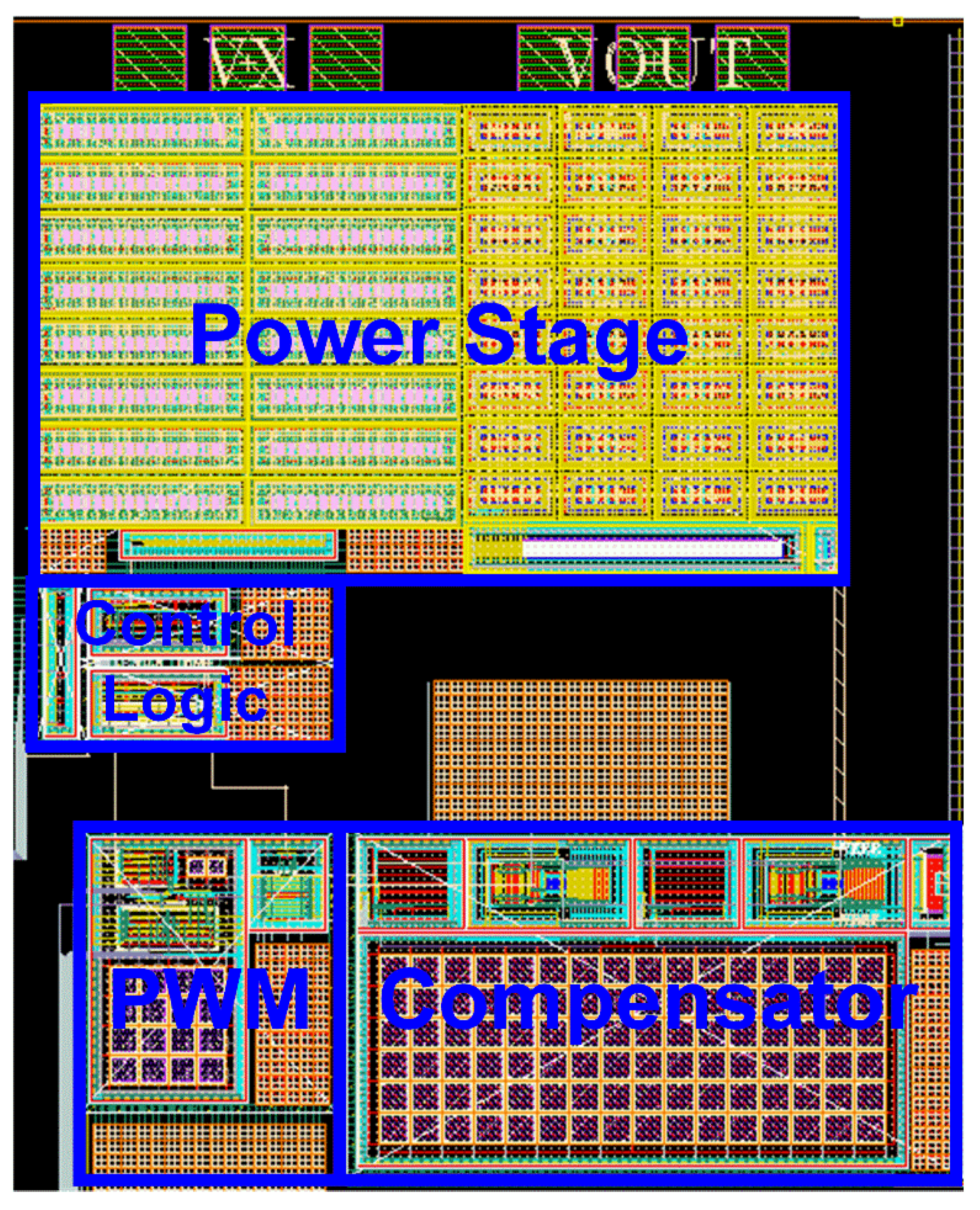
The overall layout diagram of the boost converter proposed in this study is shown in
Figure 10. It can be seen that even though the QST circuit proposed in this study is added, it can be designed with a sufficiently small area (1.2 mm
2).
4. Simulation Results
Figure 11 compares QST and CST in the boost converter based on the same voltage-mode PWM control. In brief, a load transient of 20 mA was generated every 5 µs. First, it can be seen that in the case of the prior CST, it takes two clocks until
VBIAS is fully recovered. However, it was confirmed that the case applying QST succeeded in regulation immediately except for the moment of transition. It can be seen that these results are clearly verified by the waveform of
VE. Unlike the case of CST, the range of change in
VE is kept remarkably low.
Table 1 shows the comparison results between the prior power converter ICs for high voltage generation and the boost converter proposed in this study. Since power converters optimized for SiPM have not been proposed, an exact comparison is not possible. However, we tried to evaluate the value of the proposed work by comparing it with the previously proposed step-up converters. First, that in [
9] is implemented as an SC type and can generate a relatively high voltage. However, it is not suitable for the load range of the SiPM, and it can be seen that the efficiency is also quite low. Second, the converter in [
10] can generate a high output voltage suitable for driving the SiPM, but it operates only under light load conditions when the input voltage is high (10 V). Third, the converter in [
11] is a commercial product implemented in the type of a combination of SC and SI, and it can be seen that it is relatively well designed for an SiPM. However, this also has the disadvantage that relatively many passive components are required. The DC–DC boost converter proposed in this work can supply a maximum voltage of 27 V from the nominal voltage (3.7 V) of a Li-ion battery, so it can be used in an SiPM-based radiation detection system that can be installed in a smartphone. In addition, despite operating in DCM, it is possible to stably supply a high voltage to the SiPM with a peak efficiency of up to 86%, which was calculated under post-layout simulation conditions in order to reflect the parasitic components.
5. Conclusions
In this research, a step-up DC–DC converter is proposed for optimized operation of an SiPM, which constitutes the core of the radiation detection system. In order for the SiPM to detect radiation correctly for a long time, a high voltage of at least 25 V and a current of several mA must be stably supplied from the DC–DC converter. In addition, a fast transient performance must be guaranteed at the same time, so that even high-energy radiation can be detected. Therefore, in this work, a high loop bandwidth was achieved by comparing the quadratic sawtooth waveform and the error voltage of the compensator. In particular, it was proven through the analysis and simulation that the gain bandwidth product can be increased by square root compared to when a conventional sawtooth waveform is used. Furthermore, since the proposed quadratic sawtooth waveform generator can be implemented with negligible power consumption, there is no restriction in achieving a peak efficiency of 86%. As a result, the boost converter can be applied to the mobile radiation dosimeter system, which requires high accuracy for a long time.


