Article

Electro-Optical Gas Sensor Consisting of Nanostructured Paper Coating and an Ultrathin Sensing Element

1
Laboratory of Physical Chemistry, Center for Functional Materials, Åbo Akademi University, Porthaninkatu 3-5, FI-20500 Turku, Finland
2
Nofima-Norwegian Institute of Food, Fisheries and Aquaculture Research, P.O. Box 210, NO-1431 Ås, Norway
*
Author to whom correspondence should be addressed.
Chemosensors 2019, 7(2), 23; https://doi.org/10.3390/chemosensors7020023
Submission received: 12 April 2019 / Revised: 26 April 2019 / Accepted: 29 April 2019 / Published: 1 May 2019
(This article belongs to the Special Issue Thin Film Based Sensors)

Abstract

:
This work describes the use of a paper substrate for electro-optical detection of toxic hydrogen sulfide (H2S) gas. For electrical detection, a chemiresistive type of gas sensor was developed. Ultrathin gold film electrodes (UTGFE) were produced by physical vapor deposition of gold on nanostructured latex-coated paper substrate. The gas-sensing film was deposited on the electrodes by inkjet printing. The sensing films were characterized by atomic force microscopy, X-ray photoelectron spectroscopy and conductometry. The sensing films showed more than seven orders of magnitude change in resistance when exposed to as low as 1 part per million (ppm) H2S gas at room temperature. Besides resistive response, the change in color of the sensing films was studied on a paper substrate, both as a function of print density of the sensing material and H2S concentration. For quantification of the analyte the red, green and blue color deconvolution was performed on the pictures of the paper strip indicator using an open source software. A clear response was obtained from the blue channel. The inexpensive disposable color strips produced on the paper substrate can be used for qualitative and quantitative detection (as low as 1.5 ppm) of H2S gas.

1. Introduction

In recent years, the interest in paper electronics has significantly increased. Paper is a low cost, flexible and environment-friendly material. Furthermore, the physico-chemical properties of paper substrate can be easily tuned. Mass-produced paper electronics can extend the use of flexible electronic applications in everyday life [1]. Several paper-based devices and electro-chemical platforms have been reported in the literature [2,3]. Ultrathin films are introduced for different applications including electronic, magnetic and electro-optical devices [4]. Ultrathin gold films are typically employed in microfabricated devices. These gold films display high electrical conductivity and optical reflectivity; moreover, they are chemically inert. The weak adhesion of ultrathin gold films to commonly used substrate materials, for instance glass and silica, is a challenge. We have earlier demonstrated mechanically stable ultrathin gold films fabricated on a paper substrate [5]. A nanostructured latex-coated paper was used as a substrate for the vacuum deposited ultrathin gold films with varying thickness. Detailed topographical, chemical, electrical and electro-chemical characterization of gold films has been reported earlier [5].
Hydrogen sulfide (H2S) is a highly flammable toxic gas and falls under the category of chemical asphyxiant, along with carbon monoxide and cyanide gases [6]. H2S has a distinctive smell like rotten eggs; however, due to the saturation of olfactory nerves, odor is not a reliable indicator of the presence of H2S. H2S above concentrations of 100 ppm poses serious health risks, including shock, irritation of the eyes and skin, as well as respiratory paralysis. Concentrations above 500 ppm are immediately fatal, as it affects the uptake of oxygen in the blood [7]. According to the National Institute of Occupational Safety and Health, the H2S concentration immediately dangerous to life is 100 ppm and the recommended exposure limit is 10 ppm for a maximum duration of 10 min [8]. An inexpensive, highly sensitive H2S sensor which can operate with low power consumption and under demanding conditions including high humidity and room/refrigeration temperatures can be employed for various applications (e.g., monitoring food spoilage, monitoring air quality in mines, as a diagnostic tool for biomedical applications, anti-terrorism and environmental control).
Commercial lead acetate-based paper strips are used for the colorimetric detection of H2S, the paper strip changing its color from white to black when exposed to as low as 5 ppm of H2S. Although the lead acetate-based paper strip is inexpensive, its use is limited by the low sensitivity and the toxicity of metallic lead. More recently, bismuth- and copper-based optical indicators were developed to detect very low concentrations of H2S in small sample volumes. These indicators are mainly used for qualitative detection of H2S in water, air or breath. Even though these indicators have good sensitivity, their shelf life is limited and must be used shortly after prepared [6,9]. Copper acetate films have been reported to react directly with as low as 1–10 ppm H2S to form copper sulfide [10]. The electrical response of drop-cast and inkjet-printed copper acetate films toward H2S has been reported by Virji et al. and Sarfraz et al. [7,11].
Inkjet printing is frequently employed nowadays to produce thin film structures and devices. Low material consumption and ease of changing and modifying the digital print patterns are the main features which makes this technique very attractive for the processing of functional materials [12]. Inkjet printing offers superior control of film thickness in the nano and micron scale and can feasibly produce high quality patterns on both hard and flexible substrates [13]. Furthermore, inkjet printing is a roll-to-roll compatible printing technique [14,15].
A schematic illustration of the developed sensing films is shown in Figure 1. In this study, an inexpensive disposable chemiresistor type H2S sensor on paper substrate was developed by inkjet printing copper acetate-based sensing films on ultra-thin gold film electrodes (UTGFE) with a thickness of 20 nm and gold electrodes (GE) with a thickness of 40 nm. The effect of the print density of the sensing material as well as surface plasma treatment on H2S sensitivity was studied. The change in color of the sensing material upon reaction with H2S due to the formation of copper sulfide was utilized to develop a simple color indicator. The change in color of the indicator when exposed to H2S was visible to the naked eye. Furthermore, concentrations as low as 1 ppm of H2S were detected with the developed chemiresistor in less than five minutes, and concentrations as low as 1.5 ppm of H2S were detected with the developed color indicator within 30 min of exposure. The response of the sensing films is based on the formation of a chemically stable copper sulfide and is irreversible.

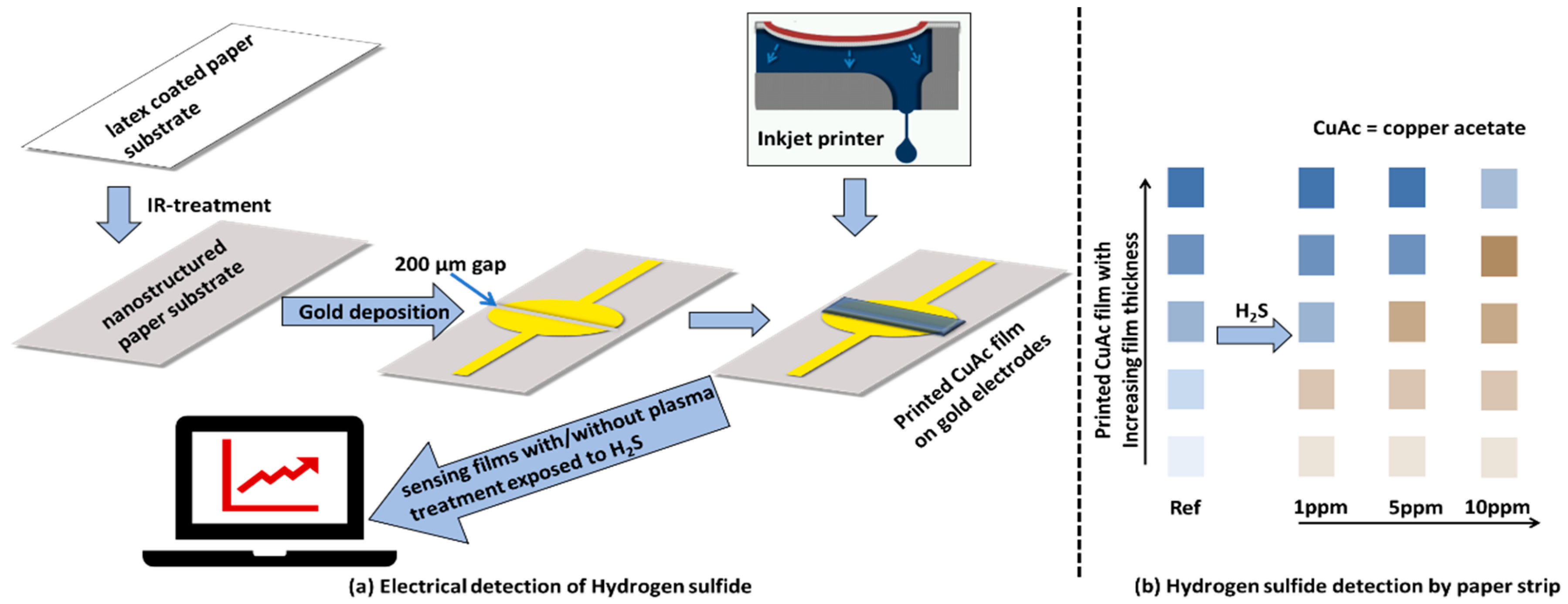
2. Materials and Methods

2.1. Paper Substrate

A barrier paper with a multi-layer structure was used to develop color strips for the detection of hydrogen sulfide. The fabrication process of the specialty paper has been explained earlier [16]. Briefly, a wood free pre-coated base paper was multilayer curtain coated. The multilayer coating was constructed to improve the barrier properties. Barrier layers mainly consisted of latex and hyper-platy barrier kaolin. The top coating consisted of binder latex and two types of kaolin pigment. The surface tension and viscosity of the coating colors was optimized using surfactants and thickeners to obtain a stable curtain. The paper substrate was calendared three times (70 bar, 70 °C) to achieve a smooth top-coating surface.

2.2. Latex-Coated Paper Substrate

Details on the fabrication and application of nanostructured latex-coated papers have been given elsewhere [17,18]. In brief, two latex components with different glass transition temperatures (Tg) were used. The low-Tg (soft) component was an emulsion polymerized carboxylated styrene butadiene acrylonitrile copolymer with Tg = 8–10 °C. The high-Tg (hard) component was modified polystyrene with Tg > 90 °C and an average particle size of 140 nm. Low-Tg and high-Tg latex components were mixed together in the weight ratio 1:1. The latex blend was applied on a pre-coated base paper by rod-coating. The nanostructured surface texture was created by irradiating the latex-coated paper with a short-wavelength infrared (IR) heater for 60 s (IRT systems, Hedson Technologies AB, Arlöv, Sweden).

2.3. Preparation of UTGF Electrodes

The physical vapor deposition method was used to fabricate gold films. A shadow mask was used for electrode patterning. The evaporation was done under high vacuum (10−6 mbar) during two separate runs, with the evaporation rate set to 12 nm/min. A deposition monitor (XTM/2, Inficon, Bad Ragaz, Switzerland) was used for gravimetric determination of the amount of evaporated gold on the latex surface. Gold films with nominal thickness of 20 nm (UTGF) and 40 nm GE were fabricated.

2.4. Inkjet Printing

The inkjet printable copper acetate-based ink was prepared by dissolving the copper acetate salt in a mixture of water, ethylene glycol (EG) and iso-propanol (IPA) with volume ratios 6.5:1.5:2. EG and IPA were used to improve the printability of the ink. Copper acetate, EG and IPA were purchased from Sigma Aldrich (Espoo, Finland). All chemicals were used as received. Inkjet printing was performed using a Dimatix Materials Printer (DMP-2831, Riihimaki, Finland). The printing was done in ambient conditions using a single nozzle with drop volume 10 pL, firing voltage 27 ± 3 V and a custom waveform to ensure optimal droplet formation. After printing, the films were left to dry at room temperature for 12 h. The films were further dried in oven at 60 °C for 1 h.

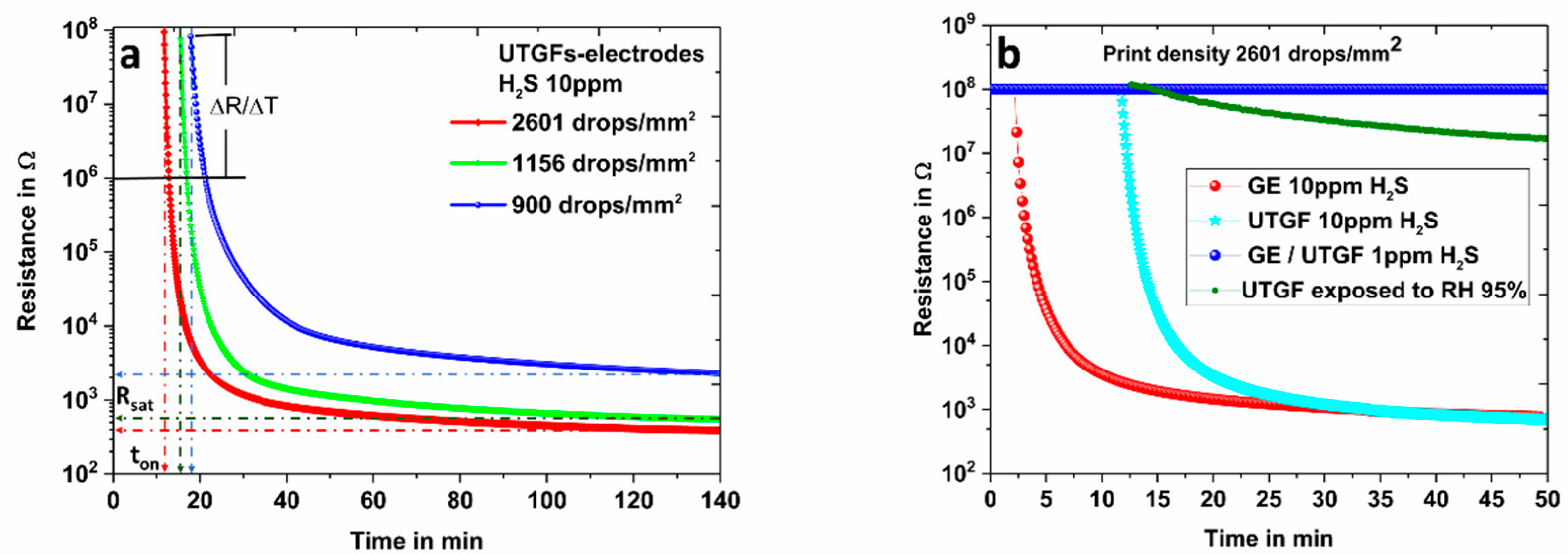
2.5. H2S Sensing Experiments

A picture of the experimental setup is shown in Figure S1 (Supplementary Materials). A gas cylinder with 200 ppm H2S gas mixture in nitrogen was used as the H2S source. An aluminum box with the dimensions 20 × 20 × 12 cm was attached to the gas cylinder. The box was equipped with four wolfram probes, an electrochemical H2S sensor (AlphaSense, with operation range of 0–200 ppm and response time <35 s), a humidity and a temperature sensor (Sensirion SHT75, with a response time of 8 s). This closed chamber was used to study the electrical and colorimetric response of the developed sensing films towards hydrogen sulfide gas under a controlled environment. The resistance of the sensing films was followed by a two-point method by connecting the probes to a digital multimeter (Keithley 2100, Köln, Germany). For plasma treatment, a Harrick plasma cleaner PDC-326 was used.

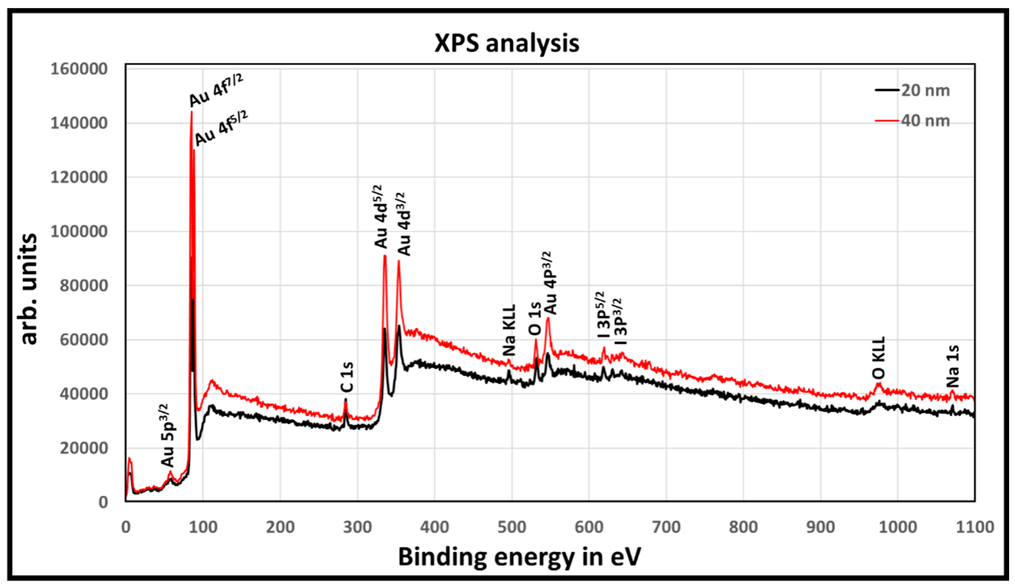
2.6. X-ray Photoelectron Spectroscopy (XPS)

XPS spectra were obtained with a PHI Quantum 2000 scanning spectrometer using a monochromatic Al Kα X-ray source (1486.6 eV), and excitation and charge neutralization by using electron filament and an electron gun. The photoelectrons were collected at 45° in relation to the sample surface with a hemispherical analyzer from approximately 5–10 nm depth into the sample. The used pass energy was 187.85 eV for survey spectra. The atomic concentration (at%) of the different elements was derived by calculating the area of the peaks and correcting for the sensitivity factors (using the software MultiPak v6.1A from Physical Electronics, Minnesota, USA).

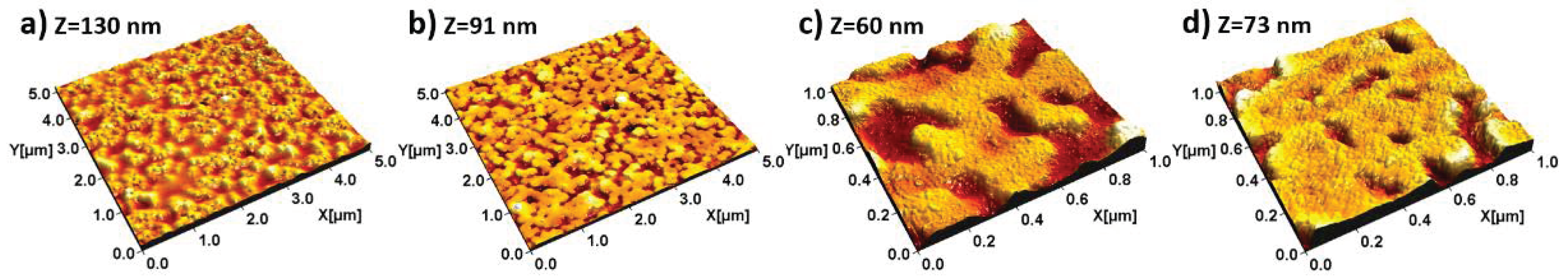
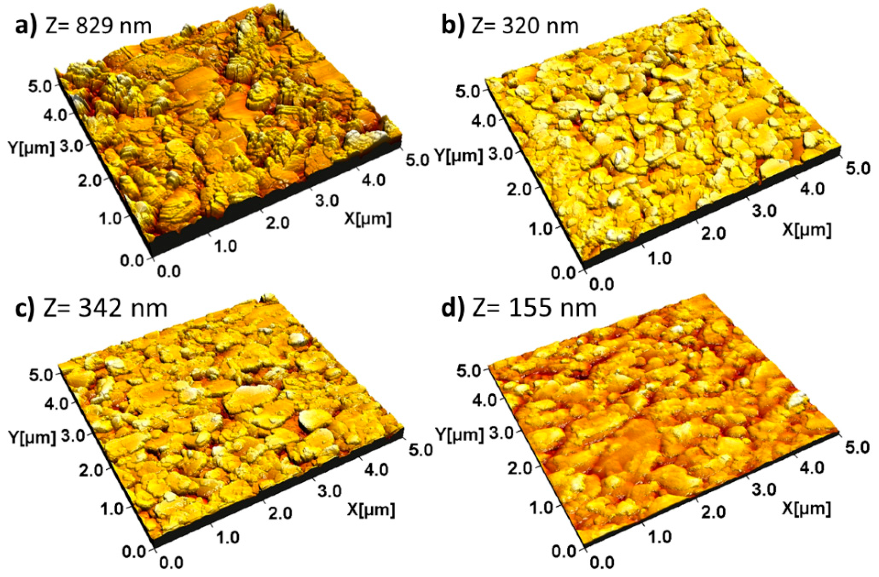
2.7. Atomic Force Microscopy

An NTEGRA PRIMA (NT-MDT, Moscow, Russia) atomic force microscope (AFM) was used for topographical analysis. The images (1024 × 1024 pixels) were captured in intermittent-contact mode in ambient conditions (T = 26 ± 2 °C, RH% = 36 ± 4) using gold coated silicon cantilevers with a nominal tip radius of 10 nm (Model: NSG 10, NT-MDT). The scanning rate and damping ratio were 0.2–0.30 Hz and 0.6–0.7, respectively. Image analysis was done using SPIP™ image analysis software (Image Metrology, Lyngby, Denmark). Z-values shown in the AFM images give the span of heights of the flattened images, that is, the difference between the highest and lowest point of the image.

3. Results and Discussion

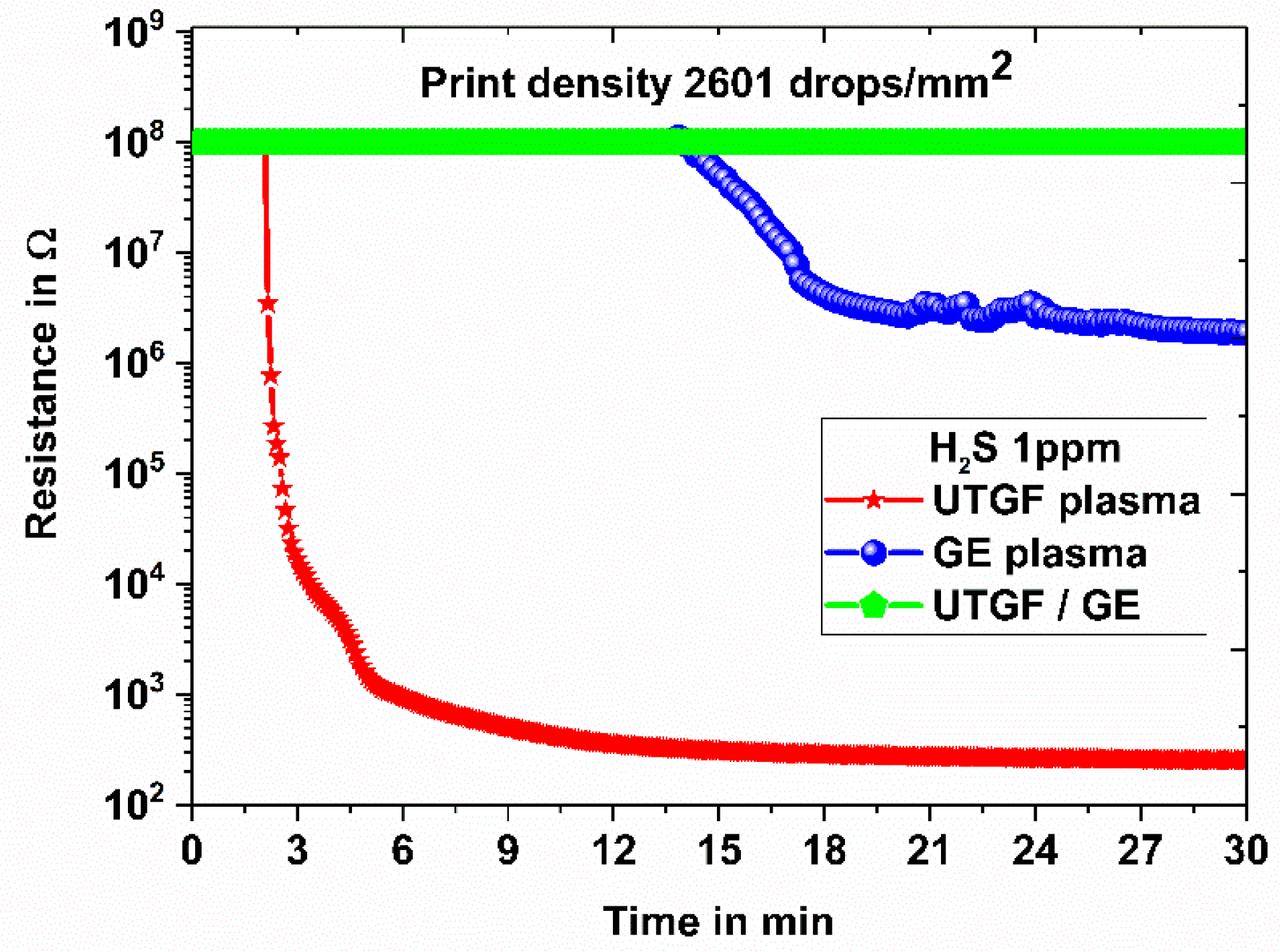
3.1. Chemiresistor Type H2S Sensor

Figure 2a,b shows AFM images of the latex-coated paper substrate before and after the IR treatment. Uniformly distributed spherical polystyrene particles can be seen in the AFM image of the paper substrate Figure 2a. Upon IR treatment of the paper substrate, a nanostructured surface was produced due to the annealing and flattening of the polystyrene particles Figure 2b. The AFM images of the UTGFE and GE deposited on the nanostructured latex-coated paper substrate are shown in Figure 2c,d, respectively. In the 1 × 1 µm AFM images, morphological differences between Figure 2c,d can be observed. In the case of UTGFE, the deposited gold film was obviously thin enough to adapt to the underlying latex nanostructure. In the case of GE, the larger amount of the deposited gold resulted in partial filling of the voids, hence somewhat fading out the latex nanostructure. Also, the grainy fine-structure of the UTGFE and GE was slightly different and apparently thickness-dependent [5].
Figure 3 shows the XPS survey spectra of the UTGFE (20 nm) and GE (40 nm). Clear peaks of Au, C and O can be seen in the spectra. Furthermore, small amounts of Na and I was also detected most likely originating from the paper substrate and the latex coating. Additionally, it can be confirmed from Table 1 that the atomic concentration of Au in the GE surface was around 55% higher compared to the UTGFE surface. Furthermore, the standard deviation (stdev) of detected Au in the case of UTGFE was higher compared to the GE (Table 1). This variation in the concentration of detected Au in the UTGFE can be explained by the fact that the deposited gold formed a very thin layer and followed the nanostructured surface of the underlaying substrate Figure 2c. In comparison, the GE film partly filled the valleys of the latex film and resulted in a smoother film with locally higher gold content Figure 2d. The relatively small standard deviation in the case of GE confirmed the formation of a more uniform film. The AFM and XPS results indicate that, in the case of the UTGFE, the grains form a continuous, interconnected island network on the surface; however, in GE, a more uniform and relatively thicker film is produced.
Figure 4a shows the electrical response of the inkjet-printed sensing films on UTGFE towards 10 ppm H2S at RH 40% ± 5 as a function of print density. Sensing films with print densities of 2601, 1156 and 900 drops/mm2 were printed. The initial resistance of the insulating copper acetate sensing films was more than 1 GΩ. After exposure to H2S, the resistance of the sensing film decreased due to the formation of semiconducting copper sulfide which is a stable compound at room temperature [7]. Clear differences among different sensing films can be seen in Figure 4a in terms of onset time of detection (ton, the time that it takes for the sensor to respond to the presence of the analyte), initial sensing kinetics (measured as ∆R/∆t) and saturation resistance (Rsat). Figure 4a shows that ton decreased from 18 to 11 min when the print density increased from 900 to 2601 drops/mm2. Similarly, improvements in the Rsat from 2324 Ω to 390 Ω and initial sensing kinetics from 21.56 × 10⁶ Ω/min to 103 × 106 Ω/min were observed when the print density was increased from 900 to 2601 drops/mm2 Figure 4a.
These improvements in ton, Rsat and initial sensing kinetics with increasing print density of the sensing film can be explained in terms of improved quality of the printed film (better coverage of the electrodes). The stability of the sensing films against humidity was also tested. The UTGFE sensor exhibited no electrical response when exposed up to RH of 80% for a period of 2 h. However, when exposed to RH of 95%, the resistance of the UTGFE sensing film decreased almost one order of magnitude over the course of 2 h, as shown in Figure 4b.
In Figure 4b, the response of the sensing film on UTGFE is compared against GE towards 10 ppm and 1 ppm H2S, respectively. There is a negligible difference between the two sensors in terms of initial sensing kinetics (103 × 106 Ω/min and 118 × 106 Ω/min) and Rsat (775 Ω and 780 Ω); however, the sensing film on the GE displayed relatively faster ton of 2 min when exposed to 10 ppm H2S. Both sensing films on UTGFE and GE did not show any electrical response when exposed to 1 ppm H2S for a period of one hour. These sensing films were then subjected to surface plasma treatment for two minutes before exposure to H2S. As shown in Figure 5, the surface plasma treatment had a substantial effect on UTGFE sensor performance compared to the GE sensor. The UTGFE sensor showed more than seven orders of magnitude change in resistance upon exposure to 1 ppm H2S with much improved sensing performance parameters. On the other hand, after the plasma treatment the GE sensor also showed a response towards 1 ppm H2S. However, the sensor response was very slow compared to UTGFE sensor in terms of ton (14 min compared to 2 min) and initial sensing kinetics (37 × 106 Ω/min compared to 399 × 106 Ω/min). Furthermore, only three orders of magnitude change in resistance was obtained from the GE sensor Figure 5.
It has been reported in the literature that the surface plasma treatment of copper acetate films can improve the sensing properties due to the formation of the oxidative products Cu2O and Cu3O2, which are suggested to explain the improved response from the GE sensor upon plasma treatment [19]. Furthermore, gold nanoparticles have been reported to have size-dependent catalytic activity. Catalytic gold nanoparticles can facilitate adsorption and dissociation of gas molecules along with enabling oxidation of gas molecules through reactive oxygen species [19]. The gold nanoparticles compared to their bulk counter parts have superior catalytic properties due to their high surface to volume ratio and chemical potential [20]. The significant improvement in the response of the UTGFE sensor upon plasma treatment is explained in terms of the catalytic properties of the UTGFEs.

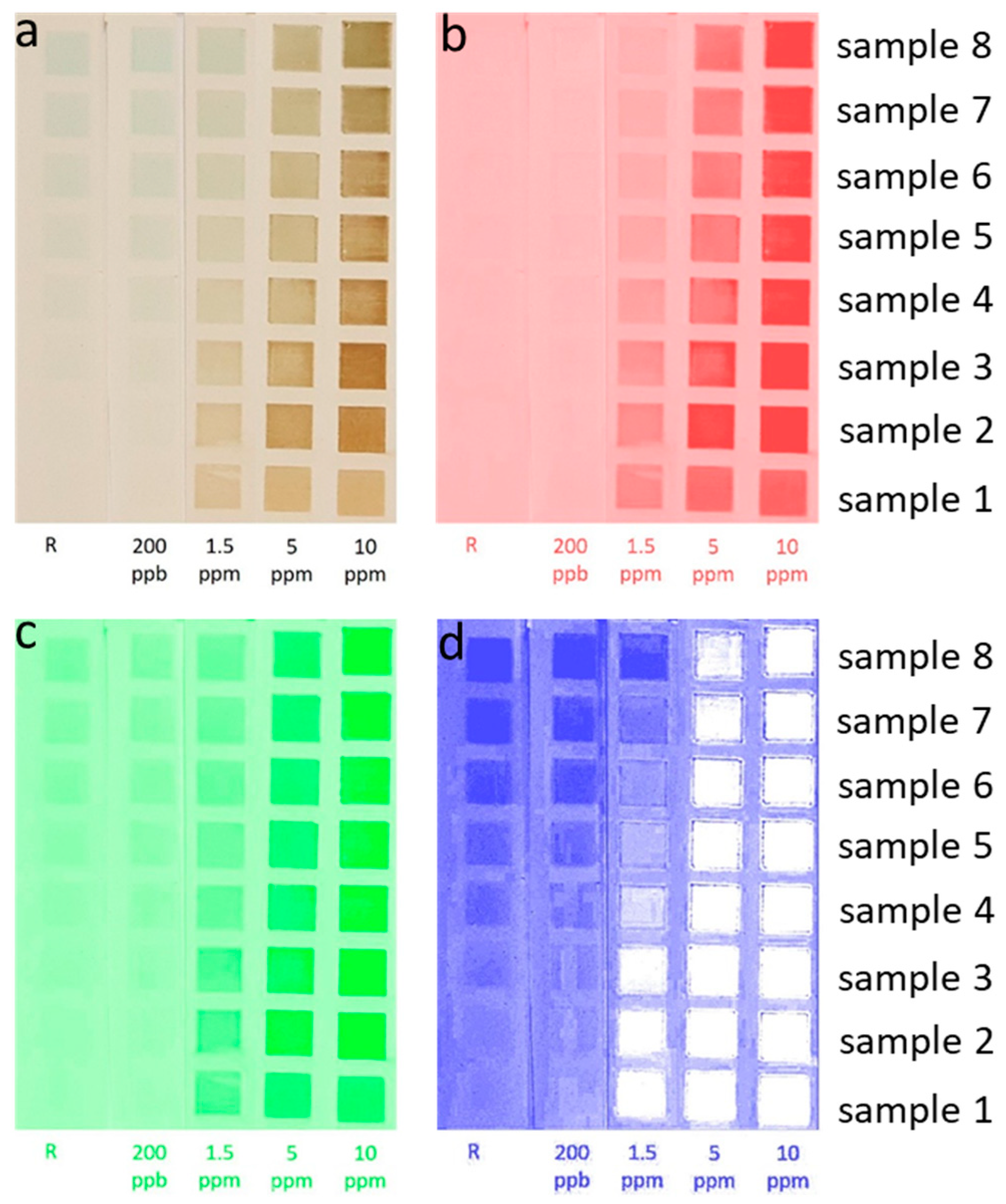
3.2. Paper Strip Indicator for H2S

Copper acetate-based ink was used to develop an inexpensive and robust color indicator on paper substrate capable of both qualitative and quantitative detection of H2S. Figure 6a shows AFM images of the kaolin-coated paper substrate. The kaolin pigment particles are clearly resolved in the image. An Sq roughness of 47 nm was calculated for this substrate.
Figure 6b–d show the AFM images of the printed copper acetate films on the paper substrate with a print density of 2028, 4056 and 6084 drops/mm2. The Sq values decreased from 47 nm (paper substrate) to 18.5 nm (film with print density of 6084 drops/mm2) as the ink filled the valleys between the kaolin particles. Furthermore, it can be seen from Figure 6d that a print density of 6084 drops/mm2 of copper acetate was enough to fill in the space between the kaolin pigment particles, though it did not make the surface fully smooth.
Different copper compounds have different characteristic colors. The change in color of copper acetate from bluish green to greyish brown copper sulfide upon reacting with H2S was utilized for the colorimetric detection of H2S. The optical response of the sensing film was studied on a paper substrate, both as a function of print density of the sensing material and H2S concentration. A set of eight films with varied print densities were produced. The print density of the copper acetate precursor for each film is listed in Table 2. Copper acetate films were exposed to different concentrations of H2S at RH 40% ± 5 for 30 min. Figure 7a shows a picture of the sensing films taken with a smartphone before and after exposure to H2S. To reduce the image analysis errors, all the exposed films and the reference copper acetate film were photographed at the same time under the same light conditions with a white background using a smartphone camera (Samsung Galaxy S6, Samsung Electronics, Suwon, South Korea). Clear changes in the color were visible after H2S exposure, even to the naked eye. For further image analysis, the picture was processed with an open source software. Figure 7b–d show the RGB color deconvolution of the original picture. Among the red, green and blue channels, the clearest response was obtained from the blue channel. It can be seen from Figure 7d that after the H2S exposure of the color strip to 1.5 ppm for 30 min, only the bottom three squares with print densities 2028, 4056 and 6084 drops/mm2 appeared white, while at 5 and 10 ppm all the squares appeared white. The color response of the paper strip can be further improved by optimizing the print density of the active material as well as the exposure time. However, here we have shown a proof of concept that a simple copper acetate-based paper strip can be utilized for quantitative detection of H2S. Furthermore, average RGB values of the sensing films (sample 1, 4 and 8) for different concentrations of H2S are given in Table S1.

4. Conclusions

This study demonstrates that a low-cost disposable electrical gas-sensing platform on paper substrate using combination of nanostructured paper coatings and ultrathin sensing element can be utilized for the electrical detection of toxic gases. Inkjet-printed sensing films based on copper acetate were developed. The electrical response of the sensing films against H2S in terms of onset time of detection, initial sensing kinetics and saturation resistance, was studied at room temperature. Both the electrical and colorimetric response of the sensing films towards H2S was studied in terms of variations in print density of the sensing film and H2S concentration. It is concluded that the print density has a significant effect on the performance of the sensing film. In addition, an ultra-sensitive gas sensor was demonstrated by optimizing the print density of the sensing film and thickness of the electrode in combination with surface plasma treatment. It is further concluded that a copper acetate-based sensing film can be used for electrical detection of as low as 1.5 ppm H2S. The RGB analysis confirmed that copper acetate-based sensing films can be potentially employed for colorimetric detection of H2S.

Supplementary Materials

The following are available online at https://www.mdpi.com/2227-9040/7/2/23/s1, Figure S1. Pictures showing the experimental setup. Table S1. Average RGB values of the sensing films on paper substrate towards different concentrations of H2S with print density of 2028 drops/mm2, 8112 drops/mm2 and 16,224 drops/mm2.

Author Contributions

Conceptualization, J.S.; methodology, J.S.; formal analysis, J.S. and E.R.; investigation, J.S., P.I. and E.R.; resources, J.P.; writing—original draft preparation, J.S.; writing—review and editing, P.I., E.R. and J.P.; supervision, P.I. and J.P.; funding acquisition, J.P., J.S.

Funding

The authors would like to thank the financial support from the Academy of Finland funding through project TWIN-A (307466), and the Functional Materials at Biological Interfaces Centre of Excellence at Åbo Akademi University. Furthermore, the authors would also like to thank the Norwegian Foundation for Research Levy on Agricultural Products (FFL) for funding through the strategic research program FoodMicro-Pack (project no 201704). Rosqvist also thanks the Tor, Joe och Pentti Borgs Minnesfond Foundation for support.

Acknowledgments

Syeda Qudsia from Laboratory of physical chemistry ÅAU Finland is acknowledged for XPS measurement.

Conflicts of Interest

The authors declare no conflict of interest.

References

  1. Bollstrom, R. Paper for Printed Electronics and Functionality. Ph.D. Thesis, Åbo Akademi University, Åbo, Finland, 2013. [Google Scholar]
  2. Tobjörk, D.; Österbacka, R. Paper electronics. Adv. Mater. 2011, 23, 1935. [Google Scholar] [CrossRef] [PubMed]
  3. Apilux, A.; Dungchai, W.; Siangproh, W.; Praphairaksit, N.; Henry, C.S.; Chailapakul, O. Lab-on-paper with dual electrochemical/colorimetric detectionfor simultaneous determination of gold and iron. Anal. Chem. 2010, 82, 1727–1732. [Google Scholar] [CrossRef] [PubMed]
  4. Lüth, H. Solid Surfaces, Interfaces and Thin Films, 5th ed.; Springer: Berlin/Heidelberg, Germany, 2010. [Google Scholar]
  5. Ihalainen, P.; Määttänen, A.; Pesonen, M.; Sjöberg, P.; Sarfraz, J.; Österbacka, R.; Peltonen, J. Paper-supported nanostructured ultrathin gold film electrodes –Characterization and functionalization. Appl. Surf. Sci. 2015, 329, 321–329. [Google Scholar] [CrossRef]
  6. Rosolina, S.; Carpenter, T.; Xue, Z. Bismuth-based, disposable sensor for the detection of hydrogen sulfide gas. Anal. Chem. 2016, 88, 1553–1558. [Google Scholar] [CrossRef] [PubMed]
  7. Sarfraz, J.; Fogde, A.; Ihalainen, P.; Peltonen, J. The performance of inkjet-printed copper acetate-based hydrogen sulfide gas sensor on a flexible plastic substrate—Varying ink composition and print density. Appl. Surf. Sci. 2018, 445, 89–96. [Google Scholar] [CrossRef]
  8. Xu, H.; Wu, J.; Chen, C.; Zhang, L.; Yang, K. Detecting hydrogen sulfide by using transparent polymer with embedded CdSe/CdS quantum dots. Sens. Actuators B 2010, 143, 535–538. [Google Scholar] [CrossRef]
  9. Carpenter, T.S.; Rosolin, S.M.; Xu, Z. Quantitative, colorimetric paper probe for hydrogen sulfide gas. Sens. Actuators B Chem. 2017, 253, 846–851. [Google Scholar] [CrossRef]
  10. Virji, S.; Fowler, J.D.; Baker, C.O.; Huang, J.; Kaner, R.B.; Weiller, B.H. PANI nanofiber composites with metal salts: Chemical sensors for hydrogen sulfide. Small 2005, 1, 624–627. [Google Scholar] [CrossRef] [PubMed]
  11. Virji, S.; Kaner, R.; Weiller, B. Direct electrical measurement of the conversion of metal acetates to metal sulfides by hydrogen sulfide. Inorg. Chem. 2006, 45, 10467–10471. [Google Scholar] [CrossRef] [PubMed]
  12. Tekin, E.; Smith, P.; Schubert, U. Inkjet printing as a deposition and patterning tool for polymers and inorganic particles. Soft Matter 2008, 4, 703–713. [Google Scholar] [CrossRef]
  13. Li, J.; Sollami, S.; Zhang, P.; Yang, S.; Lohe, M.R.; Zhuang, X.; Feng, X.; Ostling, M. Scalable Fabrication and Integration of Graphene Microsupercapacitors through Full Inkjet Printing. ACS Nano 2017, 11, 8249–8256. [Google Scholar] [CrossRef] [PubMed]
  14. Jia, H.; Gao, H.; Mei, S.; Kneer, J.; Lin, X.; Ran, Q.; Wang, F.; Palzer, S.; Lu, Y. Cu2O@PNIPAM core–shell microgels as novel inkjet materials for the preparation of CuO hollow porous nanocubes gas sensing layers. J. Mater. Chem. C 2018, 6, 7249–7256. [Google Scholar] [CrossRef]
  15. Rieu, M.; Camara, M.; Tournier, G.; Viricelle, J.; Pijolat, C.; Rooij, N.F.; Briand, D. Fully inkjet-printed SnO2 gas sensor on plastic substrate. Sens. Actuators B 2016, 236, 1091–1097. [Google Scholar] [CrossRef]
  16. Bollström, R.; Tuominen, M.; Määttänen, A.; Peltonen, J.; Toivakka, M. Top layer coatability on barrier coatings. Prog. Org. Coat. 2012, 73, 26–32. [Google Scholar] [CrossRef]
  17. Juvonen, H.; Määttänen, A.; Ihalainen, P.; Viitala, T.; Sarfraz, J.; Peltonen, J. Enhanced protein adsorption and patterning on nanostructuredlatex-coated paper. Colloids Surf. B 2014, 118, 261–269. [Google Scholar] [CrossRef] [PubMed]
  18. Juvonen, H.; Määttänen, A.; Laurén, P.; Ihalainen, P.; Utti, A.; Yliperttula, M.; Peltonen, J. Printed paper-based reaction arrays for 2D cell cultures. Acta Biomater. 2013, 9, 6704. [Google Scholar] [CrossRef] [PubMed]
  19. Sarfraz, J.; Maattanen, A.; Torngren, B.; Pesonen, M.; Peltonen, J.; Ihalainen, P. Sub-ppm electrical detection of hydrogen sulfide gas at room temperature based on printed copper acetate–gold nanoparticle composite films. RSC Adv. 2015, 5, 13525–13529. [Google Scholar] [CrossRef]
  20. Zhou, X.; Xu, W.; Liu, G.; Panda, D.; Chen, P. Size-Dependent Catalytic Activity and Dynamics of Gold Nanoparticles at the Single-Molecule Level. J. Am. Chem. Soc. 2010, 132, 138–146. [Google Scholar] [CrossRef] [PubMed]
Figure 1. Schematic illustration of the development of gas sensing film on nano-structured paper substrate for electrical detection (a) and on specialty-paper substrate for colorimetric detection (b).
Chemosensors 07 00023 g001
Figure 2. Atomic force microscope (AFM) images of the latex-coated paper substrate (a); IR-treated latex-coated paper substrate (b); ultrathin gold film electrodes (UTGFE) with 20 nm nominal evaporated gold thickness (c), and gold electrode (GE) with 40 nm evaporated gold thickness (d).
Chemosensors 07 00023 g002
Figure 3. XPS survey spectra of the UTGFE (20 nm) and GE (40 nm).
Chemosensors 07 00023 g003
Figure 4. (a) The change in resistance of UTGFE comprising of copper acetate-based sensing films with different print densities towards 10 ppm H2S as a function of time at room temperature; (b) A comparison of the electrical response of UTGFE sensor with GE sensor along with the humidity background of the UTGFE sensor.
Chemosensors 07 00023 g004
Figure 5. The effect of plasma treatment on the sensing performance of UTGFE and GE sensors at 1 ppm H2S.
Chemosensors 07 00023 g005
Figure 6. AFM images of (a) the paper substrate, and an inkjet-printed copper acetate film on this substrate with a print density of (b) 2028 drops/mm2; (c) 4056 drops/mm2; and (d) 6084 drops/mm2.
Chemosensors 07 00023 g006
Figure 7. (a) A picture of the developed colorimetric paper strip for the detection of H2S before and after exposure to different concentrations of H2S; The RGB color deconvolution of the picture using open source image analysis software to (b) the red channel; (c) the green channel and (d) the blue channel. For visualization contrast, saturated pixels are enhanced by 10%.
Chemosensors 07 00023 g007
Table 1. The atomic concentrations (at%) of detected elements are given in the table.
40 nmSample 1
at%
Sample 2
at%
Sample 3
at%
Average
at%
Stdev
Au4f4140.644.341.92.0
C1s40.24535.640.24.7
O1s14.98.816.313.33.9
I3d50.410.10.50.45
Na1s3.54.63.940.5
20 nm
Au4f22.634.624.627.26.4
C1s43.855.960.453.38.5
O1s27.3913.116.49.6
I3d51.40.61.11.00.4
Na1s4.80.10.91.92.5
Table 2. A colorimetric paper strip for H2S detection with different print densities in dops/mm2 of copper acetate films on a paper substrate.
Sample NamePrint Density in Drops/mm2
12028
24056
36084
48112
510140
612168
714196
816224

