Abstract
Nanocrystalline ZnO, ZnO(Ga), and ZnO(Ga, In) samples with different indium contents were prepared by wet-chemical method and characterized in detail by ICP-MS and XRD methods. Gas sensing properties toward NO2 were studied at 150–450 °C by DC conductance measurements. The optimal temperature for gas sensing experiments was determined. The dependence of the ZnO(Ga, In) sensor signal to NO2 at 250 °C correlates with the change of conductivity of the samples. The introduction of indium into the system leads to an increase in the values of the sensor signal in the temperature range T < 250 °C. The investigation of the local sample conductivity by scanning spreading resistance microscopy demonstrates that, at high indium content, the sensor properties are determined by the In–Ga–Zn–O layer that forms on the ZnO surface.
1. Introduction
Zinc oxide is a wide-gap semiconductor (band gap 3.4 eV), which is used as a material for transparent electrodes, optoelectronic converters, luminescent devices, catalysts, and gas sensors [1]. Non-doped zinc oxide is an n-type semiconductor. The main types of point defects are interstitial zinc atoms and oxygen vacancies, which are responsible for the deviation of the composition of Zn1+δO from stoichiometry [1,2]. For creating gas sensors, the most interesting is nanocrystalline zinc oxide with a particle size of less than 50 nm [3]. Nanocrystalline zinc oxide usually is highly resistive, since the large surface facilitates the chemisorption of acceptor molecules of oxygen. Doping of zinc oxide with M3+ cations, which can be incorporated into ZnO crystal lattice and act as donor impurities, allows increasing the conductivity of the material [4]. Trivalent cations Ga3+ and In3+ have the closest values of the effective ionic radii to that of Zn2+ [5].
The interaction with the gas phase is determined, on the one hand, by the electrophysical properties of the semiconductor oxide, and, on the other hand, by the active centers on its surface. Both these parameters, in turn, are determined by the microstructure of semiconductor oxide, the concentration of impurities, and their distribution between the volume (crystal structure) and the surface of the crystal grains of the semiconductor matrix [6]. The electrophysical properties of zinc oxide doped with gallium or indium have been widely studied in the literature [7]. Studies of the effect of impurities on active centers and the reactivity of the surface of zinc oxide are extremely few [8]. Codoping of ZnO with two donor impurities provides some additional opportunities [9,10,11,12]. Gas sensor properties of ZnO(Ga) [13,14,15,16] and ZnO(In) [17,18,19,20,21] were examined toward CO [16,19], H2S [13], NH3 [14], VOCs [18], and NO2 [13,15,17,21]. For co-doped zinc oxide in the literature, there is information only on the sensor properties of amorphous indium–gallium–zinc oxide (IGZO) films [22,23,24,25,26]. The main attention is paid to the analysis of the influence of the film synthesis temperature, measurement temperature, and effect of UV radiation on the sensor characteristics in the detection of ozone [22,23], VOCs [24], NO2 [25,26], and H2 [26].
In this work we investigated nanocrystalline ZnO(Ga, In) materials as gas sensors for the detection of NO2 at sub-ppm concentration.
2. Materials and Methods
Nanocrystalline ZnO(Ga, In) powders were synthesized by the co-precipitation method [13]. Zn(NO3)2 (1.2 M), Ga(NO3)3 (0.2 M), In(NO3)3 (0.25 M), and NH4HCO3 (1.9 M) solutions were used. To obtain ZnO(Ga, In) powders, the ratio of gallium to zinc (1 at.% [Ga]/([Ga] + [Zn])) was fixed, the indium content varied in the range 0–5 at.%. The mixture solution of metal nitrates was slowly added to a stirred solution of NH4HCO3 at 60 °C. After aging for 1 h at room temperature, the precipitate was centrifuged, washed with deionized water, dried at 50 °C for 24 h, and then calcined at 250 °C for 24 h.
The composition of the samples was determined by the inductively coupled plasma mass spectrometry (ICP-MS) on a quadrupole ICP mass spectrometer Agilent 7500c [27]. 69Ga and 71Ga, 113In and 115In, and 66Zn and 68Zn isotopes were used for analytical measurements in order to control the possible interferences and matrix effects. To obtain sample solutions, preweighed powder samples were dissolved in 1 mL nitric acid (65%, Suprapur grade) and diluted 1000 times by high-purity water (Milli-Q purification unit). Throughout this paper, the composition of the powders will be given as the ratio [M]/([Ga] + [In] + [Zn]) × 100% (at.%), M = Ga, In (Table 1).

Table 1.
Composition of the samples determined by ICP-MS.
The phase composition of the samples was determined by X-ray diffraction (XRD) using DRON-3 M instrument (CoKα radiation, λ = 1.7903 Å). The crystallite size (dXRD) of ZnO was estimated from the broadening of the (002) XRD peak using the Scherrer equation.
Concentration of surface hydroxyl groups was characterized by FTIR using a PerkinElmer Spectrum One spectrometer. FTIR spectra were recorded in transmission mode in the 400–4000 cm−1 wavenumber region with resolution of 4 cm−1. Powders (about 5 mg) were ground with 100 mg of KBr and pressed into pellets.
For the electrophysical and gas sensor measurements, the powders were mixed with a vehicle (α-terpineol in ethanol) and deposited in the form of thick films over alumina substrates with Pt electrodes on the top side and Pt heater on the back-side. The films were dried at 30 °C for 24 h and sintered at 450 °C for 10 h in air. Investigations of gas sensor properties of materials in the presence of 0.7 ppm NO2 were carried out in a flow cell under controlled constant flux of 100 mL/min by in situ measuring the electrical conductivity in DC mode (U = 3 V). The gas streams providing a predetermined composition of the gas mixture were maintained by means of electronic mass-flow controllers (Bronkhorst). The background atmosphere was obtained from a pure air generator. All measurements were effectuated in dry conditions (RH = 1%).The response S of the sensor was calculated as S = (Rgas − Rair)/Rair, where Rgas-resistance of the sample in the presence of NO2 and Rair-resistance in pure air. For each measurement temperature, four consecutive cycles of changing the gas phase composition were carried out. This allowed us to determine the average value and the error in the measurement of the sensor signal.
3. Results and Discussion
According to XRD patterns (Figure 1a) all the samples contain only ZnO (wurtzite) phase. No gallium- or indium-containing phases were detected. The quality of the diffraction patterns does not allow the accurate determination of ZnO unit cell parameters necessary to confirm the formation of ZnO-based solid solutions. The increase of impurity content leads to the broadening of XRD peaks indicating the decrease of ZnO grain size (dXRD) (Figure 1b) due to segregation of amorphous Ga- and In-containing phases on the surface of ZnO grains [12,13].
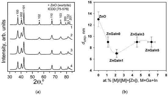
Figure 1.
(a) XRD patterns of Zn(Ga, In) powders: (1) ZnGaIn0, (2) ZnGaIn1, (3) ZnGaIn3, (4) ZnGaIn5; (b) The dependence of ZnO grain size dXRD calculated from the broadening of the (002) XRD peak on donor impurity content.
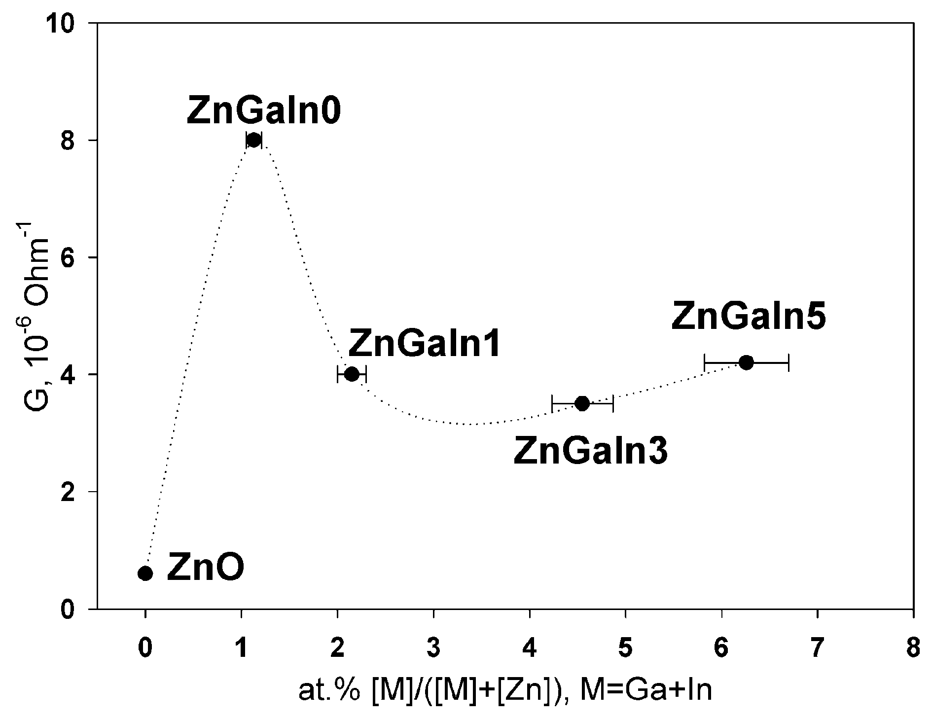
The dependence of ZnO(Ga, In) thick films conductance on impurity content is presented in Figure 2. The single doping with gallium (1.2 at.%) leads to the growth of ZnO conductance. Both Ga and In act as donor impurities in zinc oxide if occupy Zn cation sites in the ZnO lattice according to the quasi-chemical reaction (Kröger–Vink notation of point defects is used) [1]
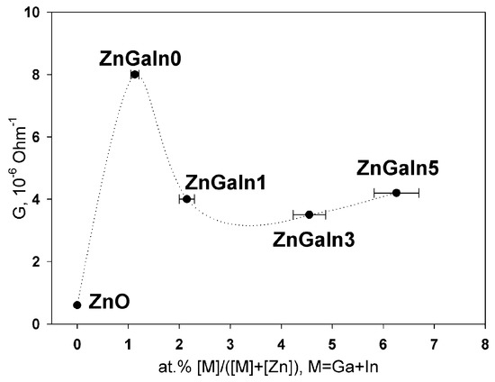
Figure 2.
The dependence of thick films conductance G as a function of donor impurity.
In the case of nanocrystalline ZnO(Ga, In) powders, an increase in the indium content leads to a slight decrease in the conductance of the material compared to the ZnGa1In0 sample. This dependence can be explained on the basis of the fact that at a donor impurity concentration of 1 at.%, the solubility limit of Ga and In in the ZnO structure is reached [13]. In cases when the total concentration of cations of Ga3+ and In3+ exceeds 1 at.%, the excess cations occupy other positions in the structure of zinc oxide (with the formation of neutral or acceptor complex defects) or form segregation of M-containing phases on the surface of ZnO(M) grains. The effective ionic radii of Zn2+, Ga3+ and In3+ for coordination number 4 in wurtzite structure are 0.60, 0.47 and 0.62 Å, respectively [5], the mismatches to Zn2+ radius are −22% for Ga3+ and +3% for In3+. So, one can expect a greater solubility of In3+ in ZnO crystal structure as compared with Ga3+. The increase in the resistivity of ZnO(Ga, In) in comparison with ZnO(Ga) with the same gallium content can be due to the fact that part of the cations of Ga3+ are dumped by In3+ cations in the joint doping. As has been shown for the ZnO(Ga) system [13], an increase in the Ga content, which is not included in the crystal structure, leads to an increase in the resistance. The absence of a significant change in the resistance with increasing indium content is due to the reasonably good conductivity of possible In-containing phases on the surface of ZnO grains. Thus, it can be assumed that both the gallium and indium enter the wurtzite crystal structure in the case of ZnO (Ga, In) samples, and they are distributed in a complex manner between the volume and the surface of the grains of nanocrystalline powders.
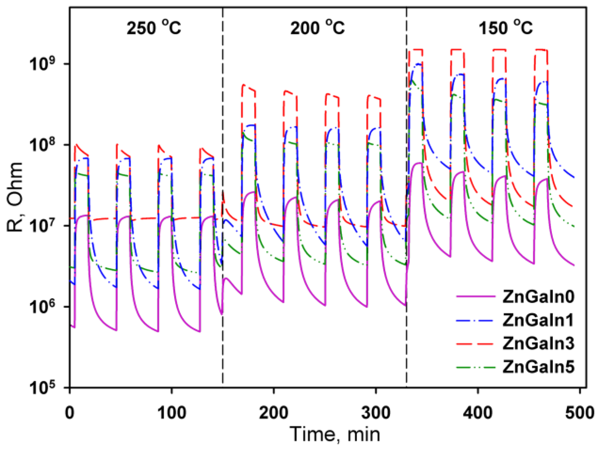
In the presence of NO2 in air, the sample’s resistance increases (Figure 3) due to acceptor gas adsorption
where is the NO2 molecule in the gas phase, is an electron from the conduction band of the semiconductor, is free surface site, is adsorbed form of NO2 (nitrite ion) on the semiconductor surface.

Figure 3.
The resistance response of ZnO(Ga, In) samples to 0.7 ppm NO2 at operating temperature 250–150 °C.
Using the law of acting masses, for the equilibrium (2) one can write
where is the total concentration of adsorption sites on the surface of the oxide (occupied and free), is NO2 partial pressure in the gas phase, is electron concentration in the near-surface layer, is concentration of adsorbed nitrite ions, is the rate constants of adsorption and desorption of nitrogen dioxide, respectively. Equation (3) shows the relationship between the concentration of NO2 in the gas phase, the degree of surface filling with chemisorbed nitrite ions, and the concentration of electrons in the near-surface layer that determines the resistance of the material. With a decrease in the concentration of NO2 in the atmosphere (in pure air), equilibrium (2) shifts to the left, which leads to a decrease in the concentration of surface nitrite ions and a decrease in the resistance of the semiconductor oxide.
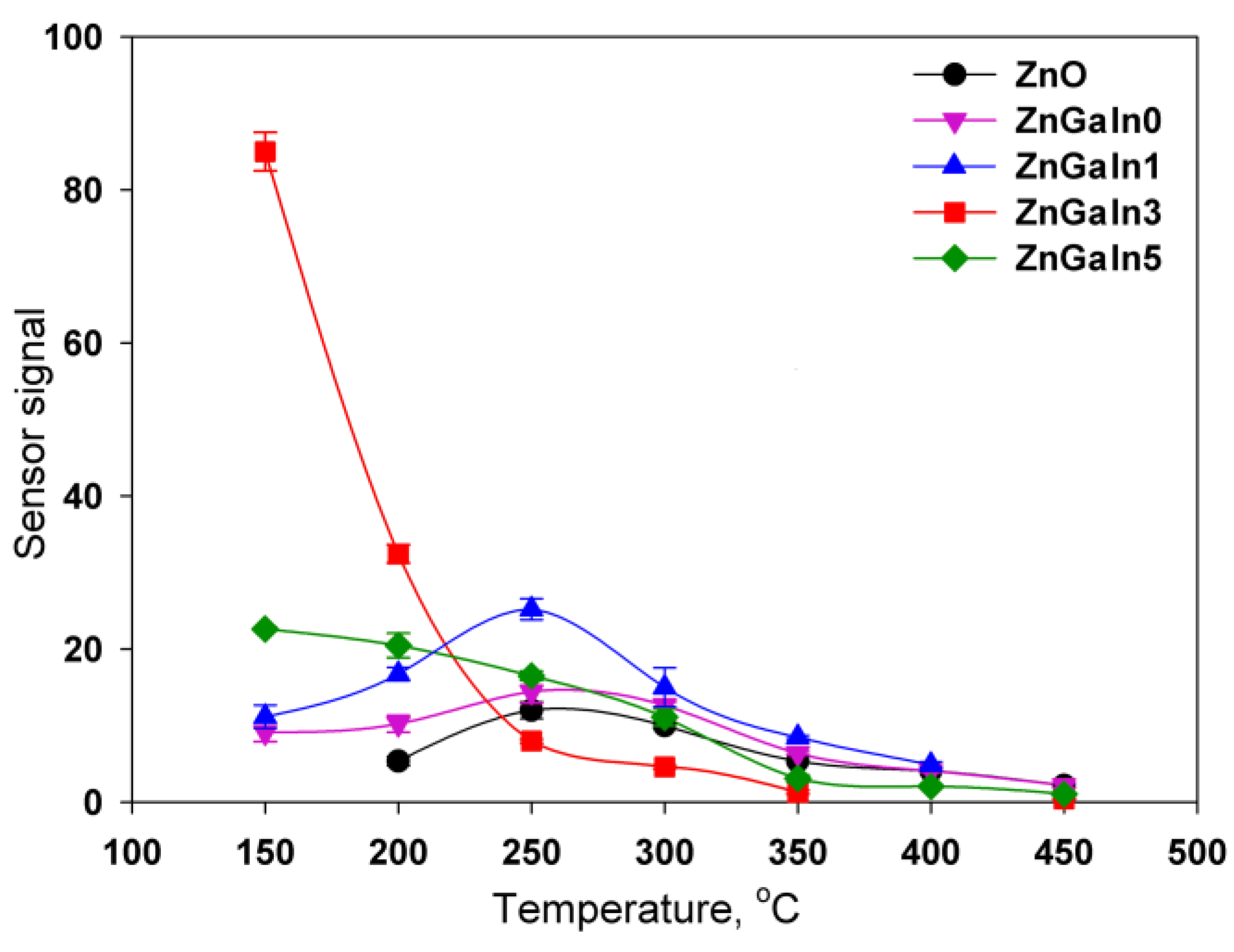
The temperature dependences of the sensor signal for all samples have a maximum. The increase in the sensor signal with decreasing temperature is due to the displacement of the adsorption–desorption equilibrium of nitrogen dioxide towards adsorption. The decrease in the signal with a further decrease in the measurement temperature is because of kinetic difficulties in the relaxation of the resistance to the initial value in the absence of NO2. For ZnO and ZnGaIn0 samples the maximum sensor signal was observed in the temperature interval 250–300 °C (Figure 4). The introduction of a minimum amount of indium (1.12 at.%) leads to the increase of sensor signal to NO2 while the form of the temperature dependence remains the same. An increase in the concentration of indium to 3.5 at.% is accompanied by the principal change in the form of the temperature dependence of the sensor signal: the maximum of the signal is shifted vs. lower temperatures, the signal value at T = 150 °C increases significantly. A further increase in the In concentration up to 5.3 at.% results in a decrease in the signal value at T = 150 °C, but the form of the temperature dependence as a whole does not change. Lowering the measurement temperature (<150 °C) leads to an increase in the resistance of the samples in the presence of NO2 up to 1.5 × 10⁹ Ohm, which is the limit of the measuring system. This made it impossible to unequivocally determine the temperature corresponding to the maximum sensor signal for ZnGaIn3 and ZnGaIn5 samples.
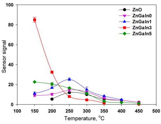
Figure 4.
Temperature dependencies of sensor signals to 0.7 ppm NO2 for ZnO(Ga, In) samples.
This situation can be explained by the distribution of indium and gallium between the crystal structure and the surface of ZnO grains, which influences the gas sensor properties through both electronic and chemical factors. As discussed above, in the case of indium, the higher solubility in zinc oxide could be expected as compared to gallium that leads to the displacement of gallium cations to the surface of zinc oxide grains. Gallium-containing phases are highly resistive semiconductors with the wide band gap Eg (4.4 ± 4.7 eV for ZnGa2O4 and 4.9 ± 5.0 eV for Ga2O3 [28]). The increase in indium concentration also results in the segregation of indium-containing amorphous phases In2O3, Zn5In2O8, and Zn3In2O6, which in contrast to Ga-containing phases, are more conductive than zinc oxide [29]. Finally, the surface of ZnO grains represents a complex composition formed by In–Ga–Zn–O layer, containing different n-n heterojunctions. These n-n junctions transfer electrons into the lower-energy conduction band, forming an “accumulation layer” in the corresponding phase [30]. The accumulation layer can be depleted by NO2 adsorption, increasing the potential energy barrier at the interface, and enhancing the sensor response (electronic factor).
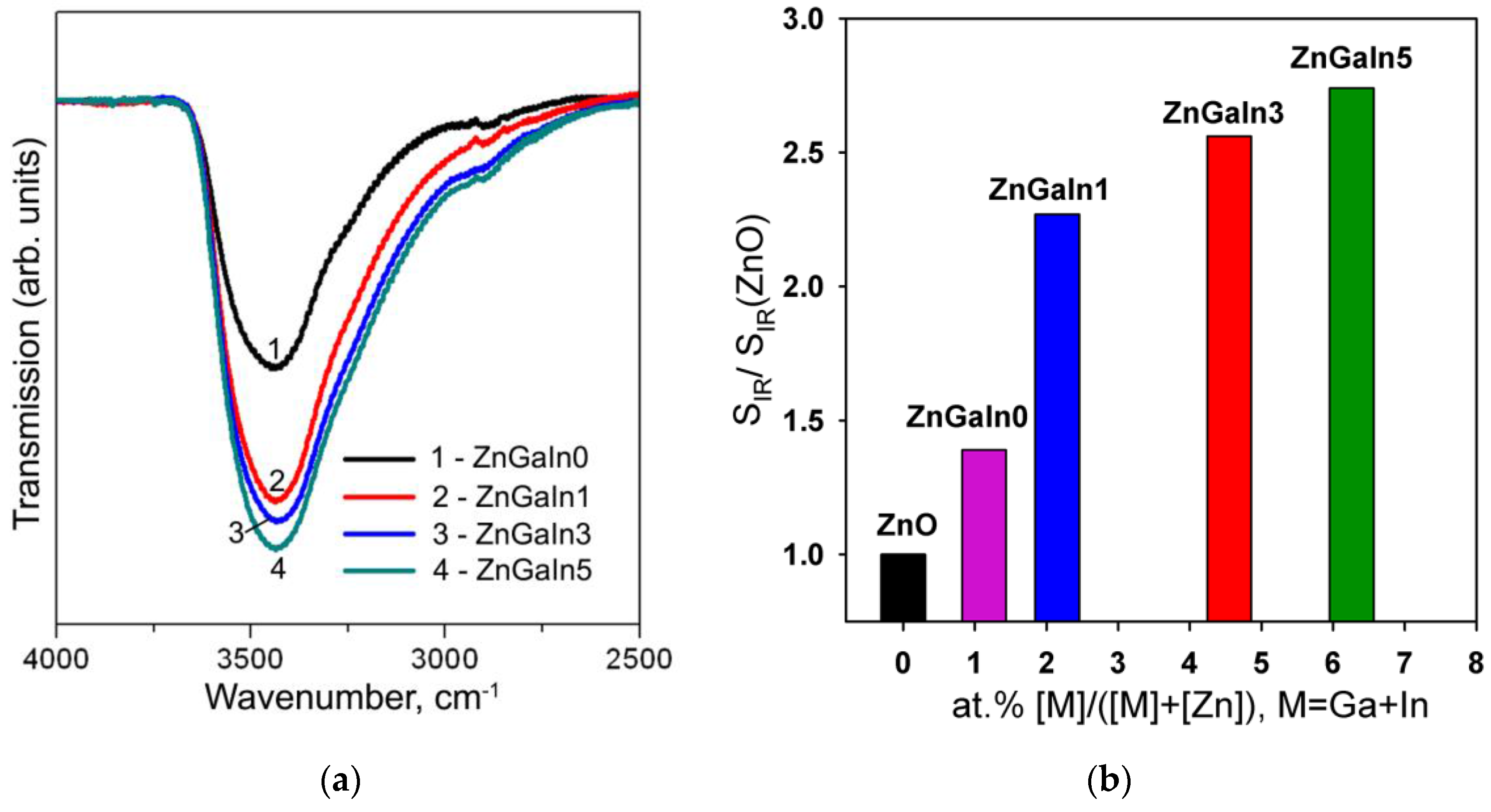
The influence of the chemical factor is manifested in a change in the concentration of surface hydroxyl groups and in the change in the predominant form of chemisorbed oxygen. The formation of surface hydroxyl groups is confirmed by IR spectroscopy. Figure 5a shows the IR spectra of investigated samples in the spectral region 2500–4000 cm−1 corresponding to the stretching vibrations of surface hydroxyl groups. For the convenience of comparing the intensities of the peaks, background lines were subtracted from the spectra, and the transmission coefficient was normalized to the peak of the lattice vibrations of the Zn–O bonds (420–460 cm−1, not shown on the figure). With increasing impurity concentration, an increase in the intensity of stretching vibrations of hydroxyl groups is observed (Figure 5b). The greatest increase in the number of hydroxyl groups occurs when a minimum amount of indium is introduced into the system. Taking into account that the Lewis acidity of the cations grows in the raw Zn2+ < In3+ < Ga3+ [31], the observed effect can be caused by the displacement of gallium on the surface of crystalline ZnO grains. As it was shown for the SnO2-based materials [6], the increase of surface acidity (e.g., in SnO2-V2O5 nanocomposites) results in the decrease in the sensor signal toward NO2.
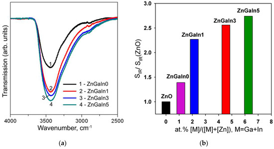
Figure 5.
(a) IR spectra of investigated samples in the spectral region 2500–4000 cm−1: (1) ZnGaIn0, (2) ZnGaIn1, (3) ZnGaIn3, (4) ZnGaIn5; (b) The dependence of the concentration of surface hydroxyl groups, represented as a peak area corresponding to OH stretching vibrations (SIR) normalized to the corresponding value for bare ZnO (SIR(ZnO)), on impurity content.
In addition to increasing the concentration of Brønsted acid sites (OH groups), the dopants contribute to a change in the route of oxygen chemisorption on ZnO surface in the temperature range 100–250 °C [8]. While, for bare ZnO, the predominant adsorbed species are atomic chemisorbates, the fraction of molecular form of chemisorbed oxygen on the sample surface increases with increasing dopant concentration, especially in the case of gallium. Since oxygen and NO2 compete on the surface of semiconductor oxides for the same adsorption centers, a change in the predominant form of chemisorbed oxygen will inevitably affect the NO2 adsorption and the corresponding value of the sensor signal. Thus, the simultaneous introduction of two impurities changes the composition of the surface of the nanocrystalline zinc oxide in a complex manner. This leads to a nonmonotonic change in the sensor properties of the materials depending on the concentration of the impurity introduced, including a change in the form of the temperature dependence of the sensor signal.
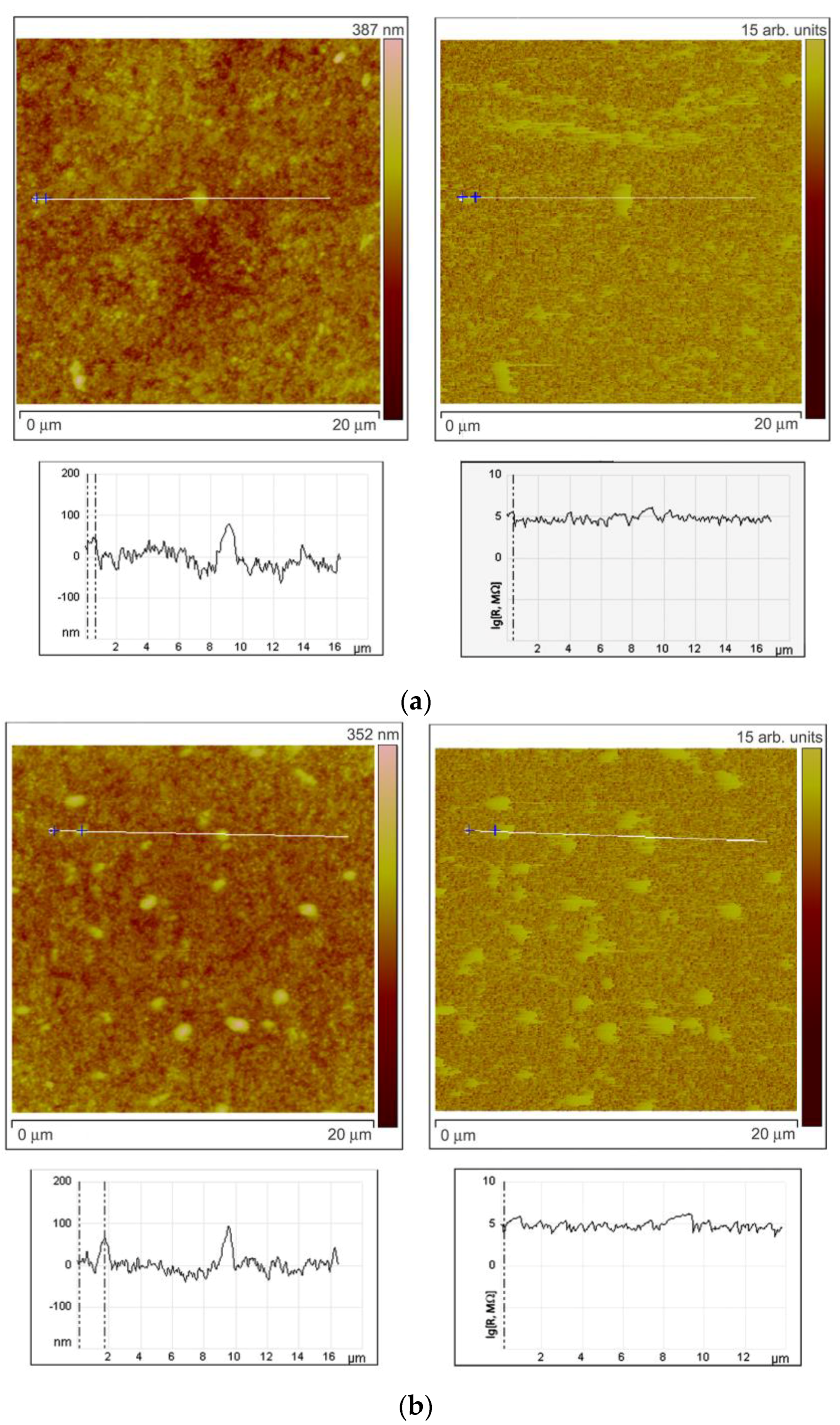
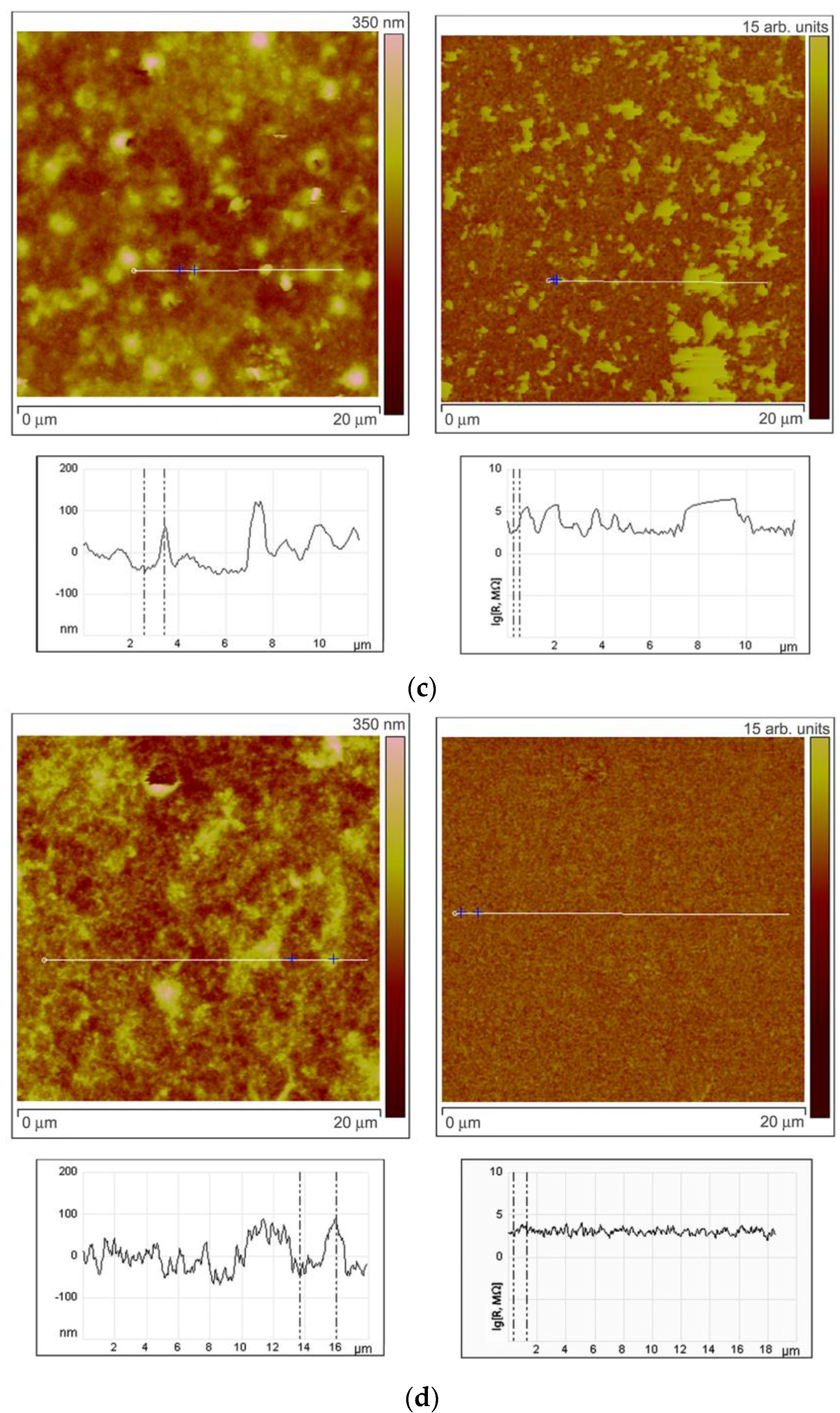
To investigate the character of element distribution on the surface of zinc oxide grains, the local resistance distribution of ZnO(Ga,In) films was studied by scanning spreading resistance microscopy (SSRM, Veeco Multimode-V scanning probe microscope). For this purpose, thin films ZnO(Ga,In) were synthesized by spin-coating technique [12]. The SSRM method enables us to measure variations in electrical conductivity or resistivity with a high spatial resolution. 1.0 V DC bias was applied between the sample and the conductive SPM tip, with the tip being on virtual ground. The sample was electrically connected to a standard sample stage using a conducting silver epoxy. Figure 6 represents the data obtained from the SSRM experiment for the ZnO(Ga,In) samples with various indium content. The sample surface topography is shown on the left side of each figure. One can see the topography image cross-section under each topographic image. The surface distribution of the local resistance is shown on the right part of each figure (SSRM images). The resistance is represented in arbitrary units on the images. The cross-section of the resistance surface distribution representing the real levels of SSRM is shown under each image.
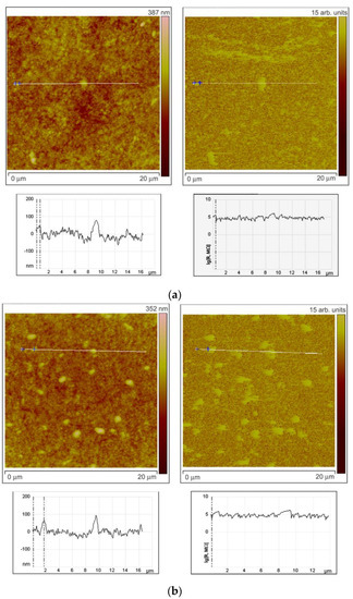
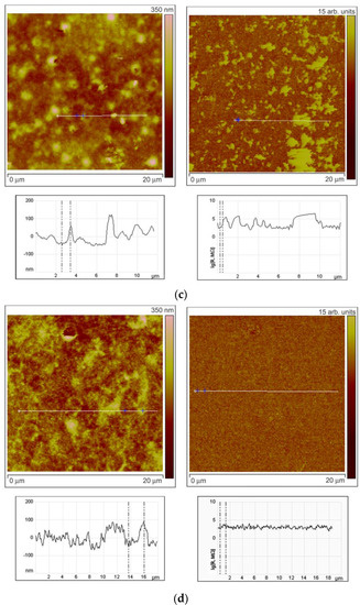
Figure 6.
Results of SSRM experiment. Surface topography with cross-sections (on the left side) and the surface distribution of the local resistance with cross-sections (on the right side) for the ZnO(Ga,In) samples containing 1.0–1.3 at.% Ga and (a) 0 at.%, (b) 0.74 at.%, (c) 3.4 at.%, and (d) 5.9 at.% In.
While the tip scans the sample in contact mode and captures data regarding the topography (left part of the figures), a current-measuring scheme senses the current passing through the sample allowing to obtain electrical information while simultaneously acquiring conventional topographical AFM data. The resulting current (I) is a measure for resistance (R) through the basic R = V/I relation (V, potential difference). The total resistance between the tip and the sample consists of a number of terms: the resistance of the small contact formed by the tip and sample (i.e., the contact resistance); the spreading resistance, which is related to the fact that the current has to spread out from the small contact into the bulk of the sample; and the resistance of the bulk material. The silicon SPM tip coated by Pt/Ir alloy was used to improve the contact. The ohmic nature of the contact was tested by the R(V) dependence measurements. To estimate the spreading resistance for the tested samples, the formula for an ideal ohmic, circular contact was used: R = ρ/4r, where r is the contact radius (25 nm for the used SPM tip), and ρ is the local sample resistivity. By measuring the resistance, one has access to the local sample conductivity (reverse resistivity).
Comparing surface topography and the SSRM images at Figure 6a,b, one can note that, at low In concentrations (0.74 at.%), the grains with high resistance can be observed on the surface as well as the lower resistance areas between the grains. The same brighter grains can be seen at the left and right images in this case and the cross-sections show that the resistance is growing more than 10 times on each mentioned grain. When In concentration was increased to 3.4 at.% the heterogeneity of the resistance surface distribution has increased (Figure 6c). Surface regions with high resistivity are observed in the images not repeating the grains distribution. At the same time, grains with high and low resistivity are also observed in this case. This situation corresponds to the highest sensor signal to NO2 at low measurement temperature of 150 °C. Figure 6d reveals the fact that the resistance of the surface becomes way more uniformly distributed at In an concentration of 5.9 at.%. The SSRM image is absolutely not repeating the surface topography in this case.
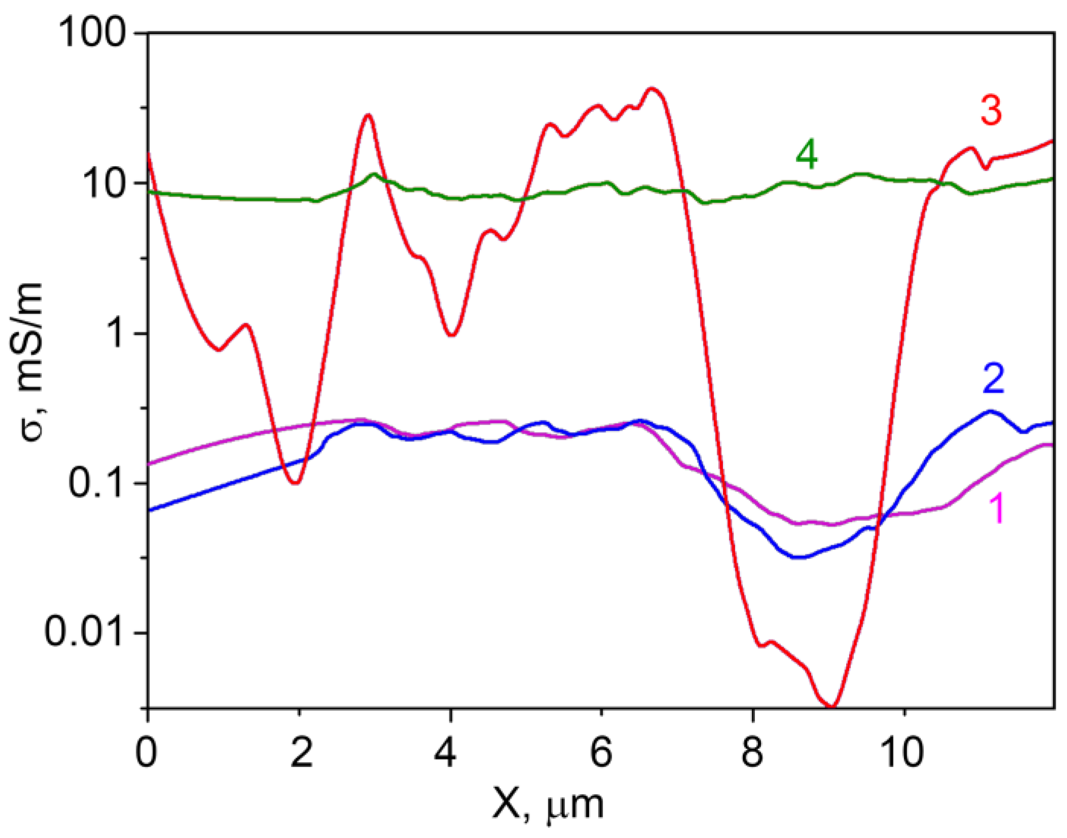
As it is seen from Figure 6, the SSRM images cross-sections contain some ‘noise’. This is due to the fact that the model used for SSRM calculation does not take into account the non-ideal contact of the microscope tip to the sample surface. When the tip shifts from the hummock to the hollow on the surface, the effective contact radius of the tip slightly changes adding some mistake to the calculations. The averaging helps to solve this problem. The distribution of averaged specific conductivity σ along the SSRM image cross-sections (calculated from the resistance cross-sections) is represented at Figure 7.

Figure 7.
Distribution of averaged specific conductivity σ along the SSRM image cross-sections of the samples containing 1.0–1.3 at.% Ga and (1) 0 at.%, (2) 0.74 at.%, (3) 3.4 at.%, (4) 5.9 at.% In.
From Figure 7, one can observe that the specific conductivity of the samples does not considerably change when concentration of indium in the sample increases from 0 at.% to 0.74 at.%, and that it is not uniformly distributed along the surface. For the sample with an In concentration of 3.4 at.%, the specific conductivity is changing along the surface much stronger than for the samples with lower indium concentrations. One can observe different regions of the sample surface with the conductivity changing more than three orders of magnitude at a distance of about 2 microns. This can be attributed to the non-uniform doping elements distribution in the sample at these concentrations. When the indium concentration in the sample is increased to 5.9 at.%, the specific conductivity distribution along the surface becomes much more uniform, indicating the increase in the homogeneity of the surface composition of zinc oxide grains. Obviously, the sensor properties in this case are determined by the In–Ga–Zn–O layer that forms on the ZnO surface.
4. Conclusions
Nanocrystalline ZnO(Ga, In) powder samples have been synthesized by co-precipitation technique. Introduction of indium into gallium doped ZnO results in nonmonotonous change in the resistivity due to the complex character of distribution of donor impurities between the crystal structure and the surface of ZnO grains. The change in the In concentration has the greatest effect on the sensor signal value at the lowest measurement temperature of 150 °C. The investigation of the local sample conductivity by scanning spreading resistance microscopy demonstrates that, at high indium content, the sensor properties are determined by the In–Ga–Zn–O layer that forms on the ZnO surface.
Acknowledgments
This work was supported by RFBR grant 15-03-03015. The authors acknowledge partial support from the Moscow State University Program of Development for the experimental support of FTIR investigations.
Author Contributions
N.V. and M.R. contributed equally to the experimental work (materials synthesis and characterization, gas sensor measurements) and discussion of the results; D.F. performed the analysis by ICP-MS; F.S. effectuated XRD characterization; V.Z. and A.Z. performed SSRM analysis; A.G. contributed greatly to the concept and discussion of the results.
Conflicts of Interest
The authors declare no conflict of interest.
References
- Ozgur, U.; Alivov, Y.I.; Liu, C.; Teke, A.; Reshchikov, M.A.; Dogan, S.; Avrutin, V.; Cho, S.-J.; Morkoc, H. A comprehensive review of ZnO materials and devices. J. Appl. Phys. 2005, 98, 041301. [Google Scholar] [CrossRef]
- Hagemark, K.I.; Toren, P.E. Determination of Excess Zn in ZnO. The Phase Boundary Zn-Zn1+xO. J. Electrochem. Soc. 1975, 122, 992–994. [Google Scholar] [CrossRef]
- Park, C.O.; Akbar, S.A. Ceramics for chemical sensing. J. Mater. Sci. 2003, 38, 4611–4637. [Google Scholar] [CrossRef]
- Ellmer, K. Transparent Conductive Zinc Oxide and Its Derivatives. In Handbook of Transparent Conductors; Ginley, D.S., Hosono, H., Paine, D.C., Eds.; Springer: New York, NY, USA, 2010; pp. 193–263. [Google Scholar]
- Shannon, R.D. Revised Effective Ionic Radii and Systematic Studies of Interatomic Distances in Halides and Chalcogenides. Acta Cryst. 1976, A32, 751–767. [Google Scholar] [CrossRef]
- Krivetskiy, V.V.; Rumyantseva, M.N.; Gaskov, A.M. Chemical modification of nanocrystalline tin dioxide for selective gas sensors. Russ. Chem. Rev. 2013, 82, 917–941. [Google Scholar] [CrossRef]
- Ginley, D.S.; Hosono, H.; Paine, D.C. Handbook on Transparent Conductors; Springer: New York, NY, USA, 2011. [Google Scholar]
- Vorobyeva, N.A.; Marikutsa, A.V.; Rumyantseva, M.N.; Kozlovskii, V.F.; Filatova, D.G.; Gaskov, A.M. Effect of Ga and In doping on acid centers and oxygen chemisorption on the surface of nanocrystalline ZnO. Inorg. Mater. 2016, 52, 578–583. [Google Scholar] [CrossRef]
- Kirby, S.D.; Van Dover, R.B. Improved conductivity of ZnO through codoping with in and Al. Thin Solid Films 2009, 517, 1958–1960. [Google Scholar] [CrossRef]
- Chirakkara, S.; Krupanidhi, S.B. Gallium and indium co-doped ZnO thin films for white light emitting diodes. Phys. Status Solidi RRL 2012, 6, 34–36. [Google Scholar] [CrossRef]
- Suresh, A.; Wellenius, P.; Dhawan, A.; Muth, J. Room temperature pulsed laser deposited indium gallium zinc oxide channel based transparent thin film transistors. Appl. Phys. Lett. 2007, 90, 123512. [Google Scholar] [CrossRef]
- Vorobyeva, N.A.; Rumyantseva, M.N.; Vasiliev, R.B.; Kozlovskiy, V.F.; Soshnikova, Y.M.; Filatova, D.G.; Zaytsev, V.B.; Zaytseva, A.V.; Gaskov, A.M. Doping effects on electrical and optical properties of spin-coated ZnO thin films. Vacuum 2015, 114, 198–204. [Google Scholar] [CrossRef]
- Vorobyeva, N.; Rumyantseva, M.; Filatova, D.; Konstantinova, E.; Grishina, D.; Abakumov, A.; Turner, S.; Gaskov, A. Nanocrystalline ZnO(Ga): Paramagnetic centers, surface acidity and gas sensor properties. Sens. Actuators B Chem. 2013, 182, 555–564. [Google Scholar] [CrossRef]
- Vorobyeva, N.; Rumyantseva, M.; Konstantinova, E.; Grishina, D.; Gaskov, A. Inversion of NH3 sensor signal and paramagnetic centers of nanocrystalline ZnO(Ga). Procedia Eng. 2011, 25, 296–299. [Google Scholar] [CrossRef]
- Cherng, I.; Lin, S.-S.; Lin, T.-J.; Hsu, C.-L.; Hsueh, T.J.; Shieh, T.-Y. The Assessment for Sensitivity of a NO2 Gas Sensor with ZnGa2O4/ZnO Core-Shell Nanowires—A Novel Approach. Sensors 2010, 10, 3057–3072. [Google Scholar]
- Kishimoto, S.; Akamatsu, S.; Song, H.; Nomoto, J.; Makino, H.; Yamamoto, T. Carbon monoxide gas sensing properties of Ga-doped ZnO film grown by ion plating with DC arc discharge. J. Sens. Sens. Syst. 2014, 3, 331–334. [Google Scholar] [CrossRef]
- Nisha, R.; Madhusoodanan, K.N.; Vimalkumar, T.V.; Vijayakumar, K.P. Effect of Indium doping on the Gas sensing behavior of Zinc oxide films obtained by Chemical spray pyrolysis method. In Proceedings of the 1st IEEE Xplore International Symposium on Physics and Technology of Sensors (ISPTS-1), Pune, India, 7–10 March 2012; pp. 204–207. [Google Scholar]
- Qi, J.; Zhang, H.; Lu, S.; Li, X.; Xu, M.; Zhang, Y. High Performance Indium-Doped ZnO Gas Sensor. J. Nanomater. 2015, 16, 74. [Google Scholar] [CrossRef]
- Hjiri, M.; Dhahri, R.; Omri, K.; El Mir, L.; Leonardi, S.G.; Donato, N.; Neri, G. Effect of indium doping on ZnO based-gas sensor for CO Materials. Sci. Semicond. Proc. 2014, 27, 319–325. [Google Scholar] [CrossRef]
- Pugh, D.C.; Luthra, V.; Singh, A.; Parkin, I.P. Enhanced gas sensing performance of indium doped zinc oxide nanopowders. RSC Adv. 2015, 5, 85767–85774. [Google Scholar] [CrossRef]
- Lin, C.-Y.; Fang, Y.-Y.; Lin, C.-W.; Tunney, J.J.; Ho, K.C. Fabrication of NOx gas sensors using In2O3–ZnO composite films. Sens. Actuators B 2010, 146, 28–34. [Google Scholar] [CrossRef]
- Chen, K.-L.; Jiang, G.-J.; Chang, K.-W.; Chen, J.-H.; Wu, C.-H. Gas sensing properties of indium–gallium–zinc–oxide gas sensors in different light intensity. Anal. Chem. Res. 2015, 4, 8–12. [Google Scholar] [CrossRef]
- Wu, C.-H.; Jiang, G.-J.; Chang, K.-W.; Lin, C.-W.; Chen, K.-L. Highly sensitive amorphous In–Ga–Zn–O films for ppb-level ozone sensing: Effects of deposition temperature. Sens. Actuators B Chem. 2015, 211, 354–358. [Google Scholar] [CrossRef]
- Jaisutti, R.; Kim, J.; Park, S.K.; Kim, Y.-H. Low-Temperature Photochemically Activated Amorphous Indium-Gallium-Zinc-Oxide for Highly Stable Room-Temperature Gas Sensors. ACS Appl. Mater. Interfaces 2016, 8, 20192–20199. [Google Scholar] [CrossRef] [PubMed]
- Cho, N.G.; Kim, I.-D. NO2 gas sensing properties of amorphous InGaZnO4 submicron-tubes prepared by polymeric fiber templating route. Sens. Actuators B 2011, 160, 499–504. [Google Scholar] [CrossRef]
- Yang, D.J.; Whitfield, G.C.; Cho, N.G.; Cho, P.-S.; Kim, I.-D.; Saltsburg, H.M.; Tuller, H.L. Amorphous InGaZnO4 films: Gas sensor response and stability. Sens. Actuators B 2012, 171–172, 1166–1171. [Google Scholar] [CrossRef]
- Filatova, D.G.; Alov, N.V.; Vorobyeva, N.A.; Rumyantseva, M.N.; Sharanov, P.Y.; Seregina, I.F.; Gaskov, A.M. Quantification of modifiers in advanced materials based on zinc oxide by total reflection X-ray fluorescence and inductively coupled plasma mass spectrometry. Spectrochim. Acta B 2016, 118, 62–65. [Google Scholar] [CrossRef]
- Robbins, J.J.; Fry, C.; Wolden, C.A. An interrogation of the zinc oxide–gallium oxide phase space by plasma enhanced chemical vapor deposition. J. Cryst. Growth 2004, 263, 283–290. [Google Scholar] [CrossRef]
- Kurz, A.; Aegerter, M.A. Novel transparent conducting sol–gel oxide coatings. Thin Solid Films 2008, 516, 4513–4518. [Google Scholar] [CrossRef]
- Miller, D.R.; Akbar, S.A.; Morris, P.A. Nanoscale metal oxide-based heterojunctions for gas sensing: A review. Sens. Actuators B 2014, 204, 250–272. [Google Scholar] [CrossRef]
- Zhang, Y. Electronegativities of Elements in Valence States and Their Applications. 2. A Scale for Strengths of Lewis Acids. Inorg. Chem. 1982, 21, 3889–3893. [Google Scholar] [CrossRef]
© 2017 by the authors. Licensee MDPI, Basel, Switzerland. This article is an open access article distributed under the terms and conditions of the Creative Commons Attribution (CC BY) license (http://creativecommons.org/licenses/by/4.0/).


