Article

Electrochemical Etching-Assisted Fabrication of Quantum Tunneling Sensing Probes with Controlled Nanogap Width

1
State Key Laboratory of Modern Optical Instrumentation, College of Optical Science and Engineering, Zhejiang University, Hangzhou 310027, China
2
Institute of Quantum Sensing, Interdisciplinary Centre for Quantum Information, Zhejiang University, Hangzhou 310027, China
*
Author to whom correspondence should be addressed.
These authors contributed equally to this work.
Chemosensors 2023, 11(9), 480; https://doi.org/10.3390/chemosensors11090480
Submission received: 30 June 2023 / Revised: 14 August 2023 / Accepted: 29 August 2023 / Published: 1 September 2023

Abstract

:
Quantum tunneling electrical probes, consisting of a pair of nanoelectrodes with a gap width of less than 5 nm, can be used as a robust electrical sensing platform for the detection of various nanoscale objects. To achieve this, stable and gap-width-controllable electrodes are essential. Although various methods, including lithography and electrochemical strategies, have been proposed for the fabrication of tunneling electrodes, the ability to precisely control the gap width and ensure reproducibility is still lacking. Here, we report a feedback-controlled electrochemical etching approach to fabricate the tunneling electrodes with a controlled nanogap. The connected nanoelectrodes, derived from a dual-barrel nanopipette, were subjected to a controlled electrochemical etching process from a short-circuited state to a tunneling gap. The resulting tunneling electrodes exhibited solvent-response current–voltage electrical behavior, which was well fitted with the Simons model, indicating the formation of tunneling electrodes. Overall, a success rate of more than 60% could be achieved to obtain the tunneling gaps. Furthermore, to verify the function of tunneling electrodes, we used the etched-tunneling electrodes for free-diffusing protein detection, showing the potential of etched-tunneling electrodes as single-molecule sensors.

1. Introduction

Single-molecule detection methods based on electrical signals can achieve direct, real-time, and label-free monitoring of the dynamic processes of molecular events at the single-molecule level [1]. It provides a platform for exploring the detailed information of chemical and biological reaction processes, including intermediate/transient states and stochastic processes, which usually drown in traditional ensemble-average experimental methods that are crucial to chemistry, biology, and medicine research [2,3]. Among these newly developed detection technologies, the method based on the quantum tunneling effect has excellent performance in the field of single-molecule detection due to its advantages of high spatial resolution, ultra-high sensitivity, and easy integration [4].
The quantum tunneling effect refers to the transport of microscopic particles such as electrons across the potential barrier, including a nanogap, a molecule, a nano-sized insulating layer, etc. It becomes increasingly pronounced as the gap width decreases to sub-5 nm [5]. Quantum tunneling sensors, which are composed of a pair of electrodes with a gap of sub-5 nm, have recently gained considerable attention due to their label-free direct in situ sensing ability in liquid environments and the potential for on-chip integrated platforms [4,5,6,7]. When a bias voltage is applied to the electrodes, electrons transport across the gap due to the tunneling effect, generating a tunneling current. The current is dependent on the applied bias, the gap width, and the medium between electrodes [4,8]. In a typical sensing system, if a specific molecule enters the tunneling region, the tunneling current will be modulated, producing a characteristic electrical signal. The acquired signal is normally superimposed on the tunneling current, with the featured current amplitude and dwell time. By extracting and analyzing these features, specific information about the target molecule can be revealed, including the sub-molecular structure and electronic structure [4].
The fabrication of tunneling electrodes with controllable gaps is the key to quantum sensing applications. In recent years, a variety of techniques have been developed for this purpose, including scanning tunneling microscope (STM) [9,10], breaking junctions [11,12,13,14], electrodeposition [5,15], electromigration [16], and advanced lithography [17,18,19]. According to the main methods used for nanogap formation, the techniques can be divided into three main categories, including additive, subtractive, and splitting methods. The additive methods, such as electrodeposition and shadow mask deposition, mainly form nanogaps by depositing electrode materials. In subtractive methods like electron beam lithography (EBL) and focused ion beam (FIB) lithography, the electrode material is removed to create a nanogap. For splitting methods including mechanically controllable break junctions (MCBJs) and crack-defined break junctions, the nanogap is generated by the fracture of electrode material. Typically, these methods have their own priorities in fabricating the tunneling gaps and cannot combine the advantages of controllability, reproducibility, stability, and mass production. For instance, shadow mask deposition produces nanogap electrodes by depositing electrode materials and local blocking suspended masks, while the grain-like growth phenomenon of metallic electrode material will cause instability and uncontrollability of electrode gap width [20]. FIB lithography generates sub-5 nm nanogaps by directly applying ion beams to electrode materials without the need for a resistance layer or a mask. It has the advantages of being maskless and having high reliability, but the ion sputtering process may cause contamination of the electrode surface. Besides the high cost, the long time consumed also influences reproducibility [18,19,21]. MCBJ allows for the formation of tunneling electrodes with an adjustable gap width by controlling the piezo actuator and is not suitable for large-scale preparation [11,21]. Moreover, most of these fabrication methods require state-of-the-art facilities, instruments, and sophisticated processes, which leads to high costs [21,22,23]. Therefore, it is essential to develop new strategies for fabricating tunneling electrodes with a more controllable gap width and reproducibility. Meanwhile, it is worth noting that a combination of manufacturing techniques is usually utilized to create nanogaps. Recently, some novel hybrid methods have been proposed to fabricate gap-width-controllable electrodes [24,25,26]. For instance, in situ adjustable metal nanogaps can be achieved by either a lateral expandable piezoelectric sheet or a stretchable membrane [26]. These nanogaps with angstrom resolution were developed into in-plane molecular break junctions and successfully applied to measure single-molecule conductance.
Recently, we reported feedback-controlled electrochemical deposition for efficiently fabricating standalone tunneling probes, which can be used directly in solution for single-molecule detection [5]. However, this electrodeposition approach tends to form narrow gaps, making it difficult to control the gap width from the atomic contact scale to a wider scale. Here, we demonstrate an electrochemical etching-assisted method for fabricating the tunneling electrodes with stable nanogaps, which can be used either independently or as a complementary method to the electrodeposition approach. Although electrochemical etching has been widely applied in STM probe fabrication with various materials such as gold (Au) [27,28,29], platinum (Pt) [30], and tungsten (W) [31], few studies have explored its capability to directly form the tunneling gap. We used a mixed solution of potassium chloride (KCl) and potassium thiosulfate (K2S2O3) as the electrolyte and a double-electrode potentiostatic electrochemical setup as the etching strategy. We achieved a success rate of approximately 60% in fabricating the tunneling probes. We further applied our tunneling electrodes to single-molecule detection. We conducted free diffusion detection on two different protein molecules (bovine serum albumin and glucose oxidase) and obtained evident single-molecule tunneling signals. Data analysis shows that there are differences in the distribution of conductance and signal dwell time between the two proteins. The results indicate that our etched-tunneling electrodes have reliable and sensitive sensing capability at the single-molecular level in liquid environments.

2. Materials and Methods

2.1. Chemicals and Materials

The Au-plating solution, consisting of 4.4 mmol/L NH4AuSO3 dissolved in 52 mmol/L (NH4)2SO3, was purchased from Tianyue (Shenzhen, China). Potassium thiosulfate (K2S2O3), with a purity of 98%, was purchased from Chentong Biochemical Technology Co., Ltd. (Hangzhou, China). All the other reagents not mentioned above used for device fabrication and characterization in this study were purchased from Sigma Aldrich (Burlington, MA, USA). All aqueous solutions should be prepared using ultrapure deionized water (18.2 MΩ·cm at 25 °C). Dual-barrel theta-shaped quartz capillaries (Friedrich & Dimmock, Inc. (Millville, NJ, USA), 1.2 mm outside diameter (OD), 0.90 mm inside diameter (ID), 75 mm long) were used for fabricating tunneling electrodes. Copper wires were 0.25 mm in diameter and purchased from Goodfellow (Shanghai, China). Silver wires (Agar Scientific, Stansted, UK, 0.25 mm OD) were made into silver/silver chloride (Ag/AgCl) electrodes in 1 mol/L potassium chloride (KCl) aqueous solution through an electrochemical workstation.

2.2. Apparatus and Characterization

The puller we used for pulling quartz capillaries was the P-2000 laser puller from Sutter Instrument (Novato, CA, USA). All electrochemical processes in this work were conducted on a CHI760c electrochemical workstation (Chenhua Instruments Shanghai Co., Ltd., Shanghai, China). All tunneling current measurements were performed using a MultiClamp 700B (Molecular Devices, San Jose, CA, USA) operated in voltage-clamp mode. The recorded signals were filtered using a four-pole Bessel filter at 10 kHz and digitized using an Axon Digidata 1550B (Molecular Devices, San Jose, CA, USA). Data analysis was performed using custom-written MATLAB code developed in-house. During tunneling current measurements, the tunneling electrode and the amplifier headstage were placed in a Faraday cage to shield external electrical noise. The setup was placed on stable support to minimize vibrational interference. In addition, short cables and electrode connecting wires were selected in priority to minimize electrical noise. The amplifier, Faraday cage, and supporting platform were connected to the same grounding point. Morphological characterization of the electrode tip was performed by a Zeiss ULTRA-55 field-emission scanning electron microscope (Oberkochen, Germany) under an operating voltage of 10 kV.

2.3. Fabrication of Dual-Barrel Au-Deposited Nanoelectrodes

The Au-deposited probes, consisting of two proximally addressable Au nanoelectrodes in a standalone double-barrel nanopipette, were obtained according to our previous work [5]. Briefly, a theta-shaped dual-barrel quartz capillary was first laser-pulled into a sharp nanopipette using a P-2000 laser puller with a custom two-line program (First line, Heat = 850, Filament = 4, Velocity = 30, Delay = 160, Pull = 100. Second line, Heat = 860, Filament = 3, Velocity = 20, Delay = 128, Pull = 160). The two nanopores formed at the probe tip were 20~60 nm in diameter and separated by a septum of about 20 nm. Next, both barrels were filled with carbon by the pyrolytic decomposition of butane, resulting in two coplanar carbon nanoelectrodes at the tip of the pipette. Copper wires were inserted from the end of the quartz capillary, in close contact with the deposited carbon, to provide the electrical connection to the instrumentation. Carbon etching was followed and formed a pit on the carbon electrode surface. This is beneficial for the subsequent electrochemical deposition of gold and improves the stability of the final prepared tunneling electrode. Then, gold was electrochemically deposited on the carbon electrodes in a bipotentiostatic configuration until it formed the connected electrodes (>4.75 μS in conductance).

3. Results and Discussion

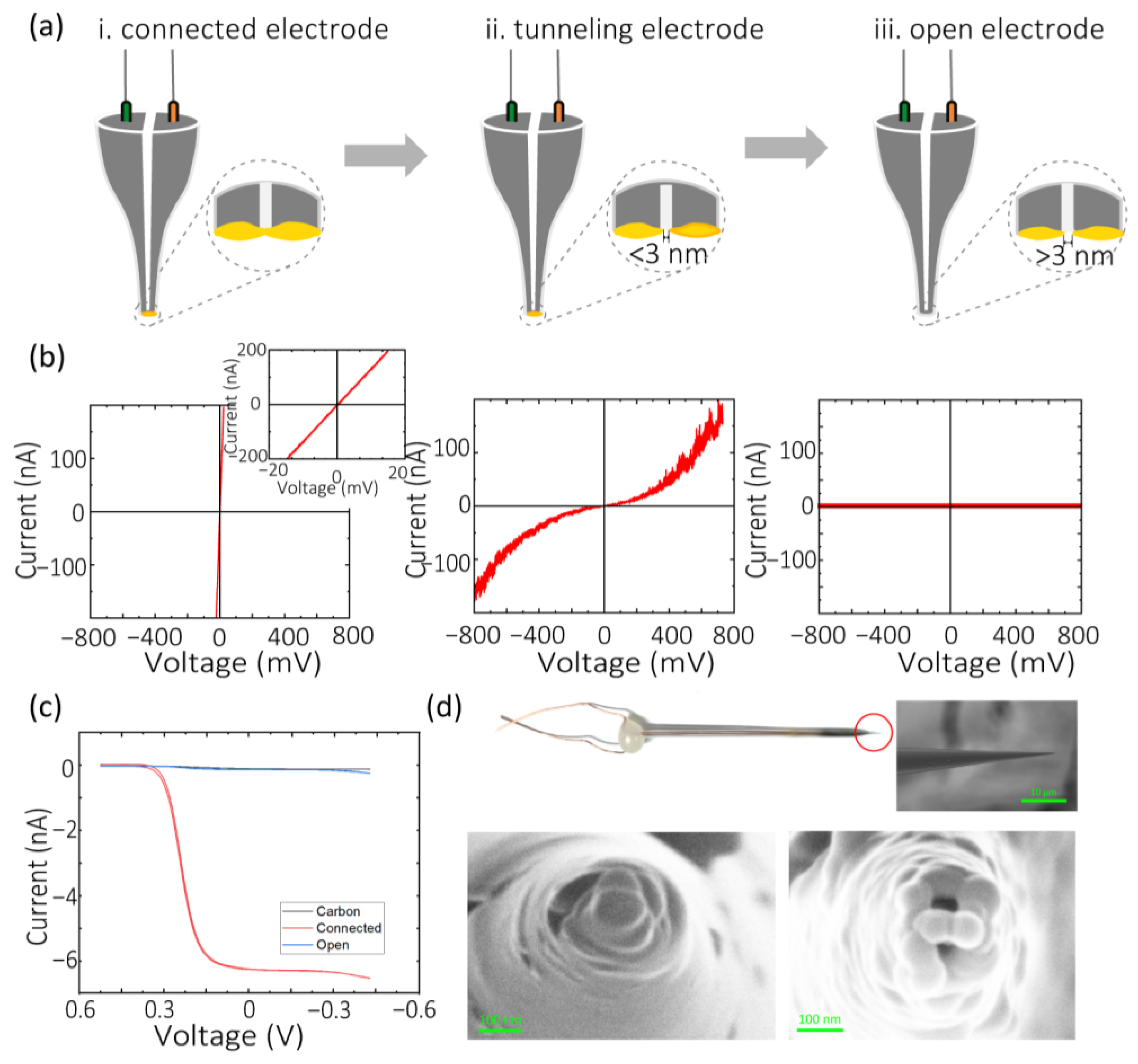
3.1. Electrochemical Etching Tunneling Electrodes Fabrication

The tunneling probes were obtained with an electrochemical etching strategy, as shown in Figure 1a. At first, the dual-barrel Au-deposited nanoelectrodes were fabricated via our previously reported method [5]. The detailed fabrication procedure has been shown above (see Section 2). Subsequently, the Au deposited on the electrodes was controllably removed to generate the tunneling gap in a double-electrode electrochemical etching configuration. In the potentiostatic electrochemical experimental setup, both of the connected electrodes were immersed in the etching electrolyte as the working electrodes (WE1 and WE2), and the silver/silver chloride electrode was used as the counter electrode and the reference electrode (CE and RE). In principle, under the presence of the etching agent potassium chloride (KCl), Au is dissolved in AuCl2 by reacting with Cl at a positive potential [32]. It should be noted that the formed AuCl2 will be partially transformed to Au (0) and AuCl4 in solution. The Au reduced by disproportionation will adhere to the electrode surface, roughening the electrode surface or even reconnecting the etched-open electrode. In order to increase the controllability of the etching process and to obtain a smooth electrode surface, we introduced the solvent potassium thiosulfate (K2S2O3) into the etching solution, which could efficiently react with the disproportionated Au and form the Au2S2O3 complex (Equation (1)) [15].
2 Au + S 2 O 3 2 Au 2 S 2 O 3 + 2 e
We further investigated the chemical composition of the etching electrolyte. The etching rate increases with the increase in the concentration of KCl. In order to control the etching rate in an appropriate range, we determined that a mixed solution containing 1 mol/L KCl aqueous solution and 2 mol/L K2S2O3 aqueous solution with a volume ratio of 4:1 is optimal.
The potentials we applied to the two working electrodes were selected based on the redox curve, as shown in Figure 1b. During the etching process, when the voltage exceeds 0.6 V, Au is oxidized to Au+ on the anode. In addition, the reaction becomes intense as the voltage increases. When the voltage reaches 1.4 V, the current oscillates due to the continuous dissolution and disproportionation reduction in Au [32], which increases the roughness of the electrode surface and makes the etching process more uncontrollable. Hence, a voltage range of 0.9 V to 1.2 V is preferred for etching. In order to obtain real-time feedback information from the current–time (It) curve and help determine the timing of etching cessation, a bias of 100 mV is set between two working electrodes. Due to the exponential correlation between tunneling current and the tunneling gap distance, the measured current containing tunneling current will sharply decrease as the gap broadens. Therefore, if a sharp decrease in measured current is observed, the etching can be stopped, which demonstrates the formation of the tunneling electrodes. Accordingly, we selected etching potentials of 1.1 V and 1.2 V for working electrode 1 (WE1) and working electrode 2 (WE2), respectively. The etching rate can be adjusted by changing the potentials of WE1 and WE2 during the etching process.
The real-time current monitoring at working electrodes revealed the etching process, as shown by the typical current curves shown in Figure 1c. Generally, the current measured at working electrodes is composed of conduction current (Iconduct, on the order of 10−6 A, under the set working potential, the same below), tunneling current (Itunneling, on the order of 10−9 A~10−6 A), and ion current (Iion, on the order of 10−10 A), such that Imeasure = Iconduct + Itunneling + Iion for WE1 and Imeasure = (−Iconduct) + (−Itunneling) + Iion for WE2. The positive and negative signs represent the direction of the current. The conduction current is generated by the directional flow of electrons between the two electrodes when they contact, and the tunneling current occurs when the electrode gap enters the tunneling range. The ion current is related to the directional flow of ions in an electrolyte solution. Due to the fact that the ion current is much smaller than the former two parts of the measured current, the currents of WE1 and WE2 exhibit symmetric changes in the curve. During the etching process, the current measured decreased with time. At the start of the etching process, the two electrodes are connected, and the conduction current is dominant under the potential difference applied to the two working electrodes. As the etching process progresses, when the electrodes are etched apart, the conduction current almost goes down to zero and the tunneling current becomes the dominant factor, which depends exponentially on the gap width. To obtain tunneling electrodes, the etching is stopped at this stage. If the etching continues, more Au will be etched away, resulting in wider gap-width electrodes.

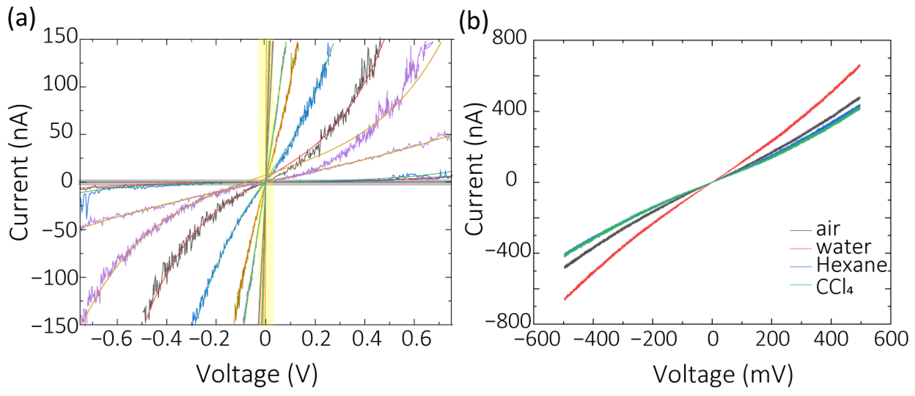
3.2. Characterization of Electrochemical Etching Electrodes

The schematic diagrams of the structure of connected electrodes, tunneling electrodes, and open electrodes are shown in Figure 2a. We performed current–voltage (IV) characterization on three types of electrodes separately. All the IV curves shown in Figure 2b had the same scale of horizontal and vertical coordinates. The connected electrodes had a large conductance (>4.75 μS), which showed up on the curve as a straight line with a very high slope. The tunneling junction showed a classical S-shape on the curve, which is the feature that represents tunneling, and the conductance typically ranged in 0.1~2 μS. The open electrode had a gap greater than 3 nm between electrodes, and the curve was almost a horizontal line on the order of 10−10 A.
Steady-state voltammetry is a reliable electrochemical method used to estimate the size of ultrasmall electrodes. This method calculates the effective radius of the electrode from the steady-state current of the electrode obtained by measuring the cyclic voltammetry curve of the redox pair. Assuming the electrode is hemispherical and the RG value (RG = rg/a, where rg is the radius of the insulator around the electrode and a is the effective radius of the electrode) is greater than 10, the effective radius can be estimated by steady-state current using Equation (2) [33].
I l i m = 2 π n e a F D c
where Ilim is the steady-state current, ne is the number of electrons transferred in electrochemical reactions, F is the Faraday constant, and D = 7.2 × 10⁻⁶ cm2 s−1 is the diffusion coefficient of [Fe(CN)6]3−. C is the concentration of the redox mediator, and a is the electrode radius. Here, we obtained the voltammograms in 10 mmol/L K3[Fe(CN)6] using the standard three-electrode system. Figure 2c shows typical curves of the same electrode in the carbon electrode state, connected state, and etched-open electrode state. The estimated effective radius of carbon electrodes, connected electrodes, and open electrodes is 23 nm, 1540 nm, and 25 nm, respectively. The size of the etched-open electrode is similar to the initial carbon electrode size, indicating that the gold on the electrode surface can be effectively etched away. The tips of the electrodes we fabricated are semi-elliptical in shape, with RG 1.5~2. Hence, the radius calculated by steady-state current is only an approximation of the actual electrode radius. The optical image of the tunneling electrode and SEM images of connected electrodes and open electrodes are shown in Figure 2d. The upper-right inset shows an enlarged SEM image of the tunneling electrode tip (inside the red circle). There is a lot of Au attached to the tip of the connected electrodes, and it has a relatively large area. As for open electrodes, we can see that Au on the tip has been etched away, exposing theta-shaped holes (about 50~100 nm in diameter).
We further characterized the etched-tunneling electrodes by IV curves and fitted them with the Simons model. To give an intuitive comparison, we present the typical IV curves of the connected, tunneling, and open electrodes in one graph, as shown in Figure 3a. The area on the yellow background is the typical curve of connected electrodes. The etched-open electrodes are displayed in the gray background area, and the remaining regions represent the etched-tunneling electrodes. The IV curves of the tunneling electrodes are fitted by the Simons model, and the fitted curve is represented by solid lines in the graph. Generally, the IV curves of electrodes with a smaller gap width tend to have steeper slopes and take on a more linear shape. The gap width can be obtained by fitting curves using the Simons model, and the gap width distribution of tunneling electrodes is shown in the Supplementary Materials (Figure S1). In total, 29 standalone etched-tunneling electrodes were fabricated with gap widths ranging from 1 nm to 3.5 nm.
To further confirm the functionality of the etched-tunneling electrodes, IV curves were measured in different materials with different barrier heights, including air, DI water, tetrachloromethane (CCl4), and hexane. The data for all four substances were collected by the same electrode. We measured 30 IV curves for each material. When switching electrodes from one material to another, we first dipped the electrodes in ethanol for 5 min to dissolve the residue and then kept them in the air for 2 min to evaporate the ethanol, which can reduce the impact caused by the residue on the electrode. The average IV curves fitted by the Simons model are shown in Figure 3b. According to Equation (3) [34], there is an exponential dependence between the square root of barrier height and the tunneling current.
I t u n n e l   ~   V b i a s z   exp ( A ϕ e f f z )
where Vbias is the bias potential between electrodes, A is the effective tunneling area, z is the gap width, and Φeff is the effective barrier height. That means, while using the same electrode and under the same voltage, the tunneling current is negatively correlated with the barrier height. From this point of view, the order of barrier height of hexane, DI water, and CCl4 determined by IV curves is consistent with the previous results [35], that is, ϕCCl4 > ϕhexane > ϕwater. It is worth mentioning that the Simons model fitting method can also be used to calculate the medium barrier height. However, due to cross-contamination of the electrodes, the fitting results are not accurate enough, so we chose the former method for analysis.

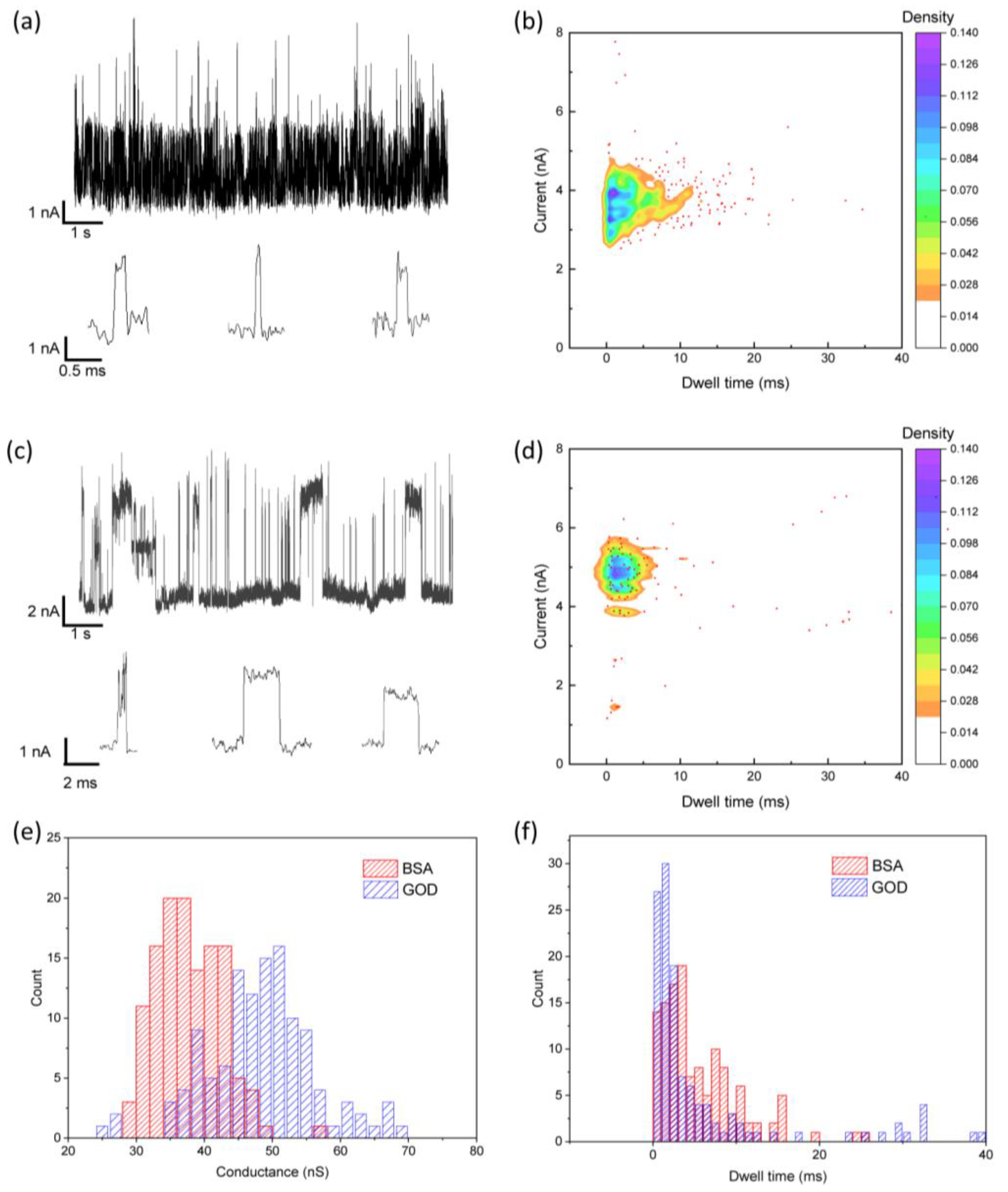
3.3. Single-Molecule Detection Using Etched-Tunneling Electrodes

In order to confirm the function of the etched-tunneling junctions, we applied the obtained quantum tunneling electrodes to single-molecule detection. Single-molecule tunneling detection methods can be divided into two categories based on whether the molecule is fixed to the electrodes: single-molecule junctions (SMJs) and molecular-free diffusion. SMJ methods bridge the molecules between two separate electrodes by chemical modification and obtain molecular conductance and other information by measuring the current. However, this method requires specific molecular modification systems, and the complexity of modification and measurements leads to low reproducibility and stability. For methods based on molecular free diffusion, the amplitude of tunneling current is related to the intrinsic properties of molecules and the interaction between electrodes and molecules [36,37]. We conducted free-diffusing single-molecule signal measurements on two protein molecules, bovine serum albumin (BSA) and glucose oxidase (GOD). BSA is the main component in bovine serum and is widely used in biochemical laboratories, with a molecular size of approximately 4 × 4 × 10 nm3. GOD is widely present in animals, plants, and microorganisms and is an important industrial enzyme in the food industry. Its molecular size is about 7 × 5.5 × 8 nm3. The size of both proteins is much larger than the gap width, so both of them cannot fully diffuse into the tunneling region.
BSA in 0.01 mol/L phosphate buffered saline (PBS, pH 7.4) with a concentration of 10 nmol/L was measured using an electrode with a gap distance of 2 nm by applying a constant voltage of 100 mV. The typical It curve and signal peak shape measured are shown in Figure 4a. The signal height that reflects the conductance of the electrode itself is about 5 nA. The pulse signal appearing indicates that BSA molecules were in or near the tunneling region, affecting electron transport and generating characteristic signals related to molecular characteristics in the measured current. The low-amplitude signals were attributed to the adsorption and desorption of small molecules by a single electrode. While the higher amplitude signals were likely caused by protein molecules bridging and binding to both electrodes, followed by desorption. For studying the conductivity of individual protein molecules, the higher-amplitude signals formed by bridging are believed to be effective, while low-amplitude adsorption signals are ignored. A statistical analysis was conducted on the signal curve with a time length of 120 s. The distribution of characteristic signal peaks and dwell time obtained is shown in Figure 4b. The signal peaks are concentrated around 4 nA, with a dwell time mostly less than 5 ms. The same experiments were conducted on 10 nmol/L GOD in a 0.01 mol/L PBS solution with an electrode with a 2.1 nm gap distance, and the typical current–time curve and signal peak shape are shown in Figure 4c. The signal height was about 2 nA. It is worth noting that the instability of the voltage applied during the measurement process can lead to a baseline offset. The signals with an apparently longer duration (>10 ms) in the figure are believed to be caused by the voltage instability between the two electrodes. Baseline fitting should be used to remove the influence of such signals during analysis. After statistical analysis, the distribution of peaks and dwell time of the signals is shown in Figure 4d, with a peak of about 5 nA and dwell time mostly below 5 ms. Figure 4e shows the histogram of the conductance distribution of BSA and GOD. The graph shows that the conductance of BSA is about 38 nS and the conductance of GOD is about 50 nS, which means the two protein molecules can be distinguished by the conductance distribution. The magnitude of the measured values of BSA conductivity is consistent with the data reported in previous reports [38,39], indicating the reliability of this method. In addition, the measured tunneling current signals of GOD obtained from the same electrode under different bias voltages (50~200 mV) were analyzed, and a predominately linear current dependence on voltage was observed with a slope of 25.77 ± 1.54 nS (Figure S2). Figure 4f shows the dwell time histograms of BSA and GOD, indicating differences in the dwell time distribution of the two proteins. The experiment results indicate the potential to differentiate proteins directly through specific tunneling signal characteristics and demonstrate the feasibility of applying this method to drug screening and biomarker detection.

4. Conclusions

In summary, we proposed and experimentally confirmed that electrochemical etching can be used independently for the fabrication of tunneling electrodes or as a complement to the electrodeposition method. We used various methods to characterize the obtained electrode, demonstrating the feasibility of the scheme. Electrochemical etching combined with electrodeposition greatly increases the success rate of electrode fabrication and improves electrode reusability. We verified the tunneling performance of the obtained electrodes by measuring the barrier heights of different substances. Moreover, we have demonstrated that the tunneling electrodes fabricated by electrochemical etching can be used in free diffusing protein molecule detection via tunneling current, which verifies the function of the fabricated quantum tunneling probes with nanogap width and shows a new strategy for developing quantum tunneling sensors.

Supplementary Materials

The following supporting information can be downloaded at: https://www.mdpi.com/article/10.3390/chemosensors11090480/s1, Figure S1: Histogram of gap width distribution for etched-tunneling electrodes; Figure S2: Tunneling current measurement of GOD under different bias voltages.

Author Contributions

Conceptualization, Q.H. and L.T.; methodology, B.S., Q.H., T.J. and L.T.; validation, B.S., Q.H. and B.Z.; formal analysis, B.S. and Q.H.; investigation, B.S. and Q.H.; resources, T.J. and B.Z.; writing—original draft preparation, B.S. and Q.H.; writing—review and editing, T.J., L.T., C.K. and X.L.; supervision, L.T., C.K. and X.L.; project administration, B.S., Q.H. and L.T.; funding acquisition, L.T. All authors have read and agreed to the published version of the manuscript.

Funding

This research was funded by the National Natural Science Foundation of China (grant nos. 62127818), the Natural Science Foundation of Zhejiang Province (grant no. LR22F050003), and the Fundamental Research Funds for the Central Universities.

Institutional Review Board Statement

Not applicable.

Informed Consent Statement

Not applicable.

Data Availability Statement

Any additional data in support of the findings of this study are available from the corresponding author upon reasonable request.

Conflicts of Interest

The authors declare no conflict of interest.

References

  1. Gu, C.; Jia, C.; Guo, X. Single-Molecule Electrical Detection with Real-Time Label-Free Capability and Ultrasensitivity. Small Methods 2017, 1, 1700071. [Google Scholar] [CrossRef]
  2. Wang, Y.; Shan, X.; Tao, N. Emerging Tools for Studying Single Entity Electrochemistry. Faraday Discuss. 2016, 193, 9–39. [Google Scholar] [CrossRef] [PubMed]
  3. Mathwig, K.; Aartsma, T.J.; Canters, G.W.; Lemay, S.G. Nanoscale Methods for Single-Molecule Electrochemistry. Annu. Rev. Anal. Chem. 2014, 7, 383–404. [Google Scholar] [CrossRef]
  4. Albrecht, T. Electrochemical Tunneling Sensors and Their Potential Applications. Nat. Commun. 2012, 3, 829. [Google Scholar] [CrossRef] [PubMed]
  5. Tang, L.; Nadappuram, B.P.; Cadinu, P.; Zhao, Z.; Xue, L.; Yi, L.; Ren, R.; Wang, J.; Ivanov, A.P.; Edel, J.B. Combined Quantum Tunneling and Dielectrophoretic Trapping for Molecular Analysis at Ultra-Low Analyte Concentrations. Nat. Commun. 2021, 12, 913. [Google Scholar] [CrossRef]
  6. Di Ventra, M.; Taniguchi, M. Decoding DNA, RNA and Peptides with Quantum Tunneling. Nat. Nanotech 2016, 11, 117–126. [Google Scholar] [CrossRef]
  7. Xin, N.; Guan, J.; Zhou, C.; Chen, X.; Gu, C.; Li, Y.; Ratner, M.A.; Nitzan, A.; Stoddart, J.F.; Guo, X. Concepts in the Design and Engineering of Single-Molecule Electronic Devices. Nat. Rev. Phys. 2019, 1, 211–230. [Google Scholar] [CrossRef]
  8. Simmons, J.G. Generalized Formula for the Electric Tunnel Effect between Similar Electrodes Separated by a Thin Insulating Film. J. Appl. Phys. 1963, 34, 1793–1803. [Google Scholar] [CrossRef]
  9. Xu, B.; Tao, N.J. Measurement of Single-Molecule Resistance by Repeated Formation of Molecular Junctions. Science 2003, 301, 1221–1223. [Google Scholar] [CrossRef]
  10. Li, X.-M.; Wang, Y.-H.; Seng, J.-W.; Zheng, J.-F.; Cao, R.; Shao, Y.; Chen, J.-Z.; Li, J.-F.; Zhou, X.-S.; Mao, B.-W. Z-Piezo Pulse-Modulated STM Break Junction: Toward Single-Molecule Rectifiers with Dissimilar Metal Electrodes. ACS Appl. Mater. Interfaces 2021, 13, 8656–8663. [Google Scholar] [CrossRef]
  11. Tsutsui, M.; Shoji, K.; Taniguchi, M.; Kawai, T. Formation and Self-Breaking Mechanism of Stable Atom-Sized Junctions. Nano Lett. 2008, 8, 345–349. [Google Scholar] [CrossRef] [PubMed]
  12. Xiang, D.; Jeong, H.; Lee, T.; Mayer, D. Mechanically Controllable Break Junctions for Molecular Electronics. Adv. Mater. 2013, 25, 4845–4867. [Google Scholar] [CrossRef]
  13. Vrouwe, S.A.G.; Van Der Giessen, E.; Van Der Molen, S.J.; Dulic, D.; Trouwborst, M.L.; Van Wees, B.J. Mechanics of Lithographically Defined Break Junctions. Phys. Rev. B 2005, 71, 035313. [Google Scholar] [CrossRef]
  14. Pan, R.; Yang, Y.; Wang, Y.; Li, S.; Liu, Z.; Su, Y.; Quan, B.; Li, Y.; Gu, C.; Li, J. Nanocracking and Metallization Doubly Defined Large-Scale 3D Plasmonic Sub-10 Nm-Gap Arrays as Extremely Sensitive SERS Substrates. Nanoscale 2018, 10, 3171–3180. [Google Scholar] [CrossRef] [PubMed]
  15. Missault, N.; Schwarzacher, W. Bridging the Nanogap: Au Electrodeposition at Parallel Electrodes with NM-Scale Spacing. J. Electrochem. Soc. 2021, 168, 082511. [Google Scholar] [CrossRef]
  16. Naitoh, Y.; Tani, Y.; Koyama, E.; Nakamura, T.; Sumiya, T.; Ogawa, T.; Misawa, G.; Shima, H.; Sugawara, K.; Suga, H.; et al. Single-Molecular Bridging in Static Metal Nanogap Electrodes Using Migrations of Metal Atoms. J. Phys. Chem. C 2020, 124, 14007–14015. [Google Scholar] [CrossRef]
  17. Manheller, M.; Trellenkamp, S.; Waser, R.; Karthäuser, S. Reliable Fabrication of 3 Nm Gaps between Nanoelectrodes by Electron-Beam Lithography. Nanotechnology 2012, 23, 125302. [Google Scholar] [CrossRef]
  18. Li, H.; Wani, I.H.; Hayat, A.; Jafri, S.H.M.; Leifer, K. Fabrication of Reproducible Sub-5 Nm Nanogaps by a Focused Ion Beam and Observation of Fowler-Nordheim Tunneling. Appl. Phys. Lett. 2015, 107, 103108. [Google Scholar] [CrossRef]
  19. Nagase, T.; Gamo, K.; Kubota, T.; Mashiko, S. Direct Fabrication of Nano-Gap Electrodes by Focused Ion Beam Etching. Thin Solid. Film. 2006, 499, 279–284. [Google Scholar] [CrossRef]
  20. Sun, L.F.; Chin, S.N.; Marx, E.; Curtis, K.S.; Greenham, N.C.; Ford, C.J.B. Shadow-Evaporated Nanometre-Sized Gaps and Their Use in Electrical Studies of Nanocrystals. Nanotechnology 2005, 16, 631–634. [Google Scholar] [CrossRef]
  21. Dubois, V.; Bleiker, S.J.; Stemme, G.; Niklaus, F. Scalable Manufacturing of Nanogaps. Adv. Mater. 2018, 30, 1801124. [Google Scholar] [CrossRef] [PubMed]
  22. Li, T.; Hu, W.; Zhu, D. Nanogap Electrodes. Adv. Mater. 2010, 22, 286–300. [Google Scholar] [CrossRef] [PubMed]
  23. He, Q.; Tang, L. Sub-5 Nm Nanogap Electrodes towards Single-Molecular Biosensing. Biosens. Bioelectron. 2022, 213, 114486. [Google Scholar] [CrossRef] [PubMed]
  24. Jeong, H.; Li, H.B.; Domulevicz, L.; Hihath, J. An On-Chip Break Junction System for Combined Single-Molecule Conductance and Raman Spectroscopies. Adv. Funct. Mater. 2020, 30, 2000615. [Google Scholar] [CrossRef]
  25. Zhang, S.; Guo, C.; Ni, L.; Hans, K.M.; Zhang, W.; Peng, S.; Zhao, Z.; Guhr, D.C.; Qi, Z.; Liu, H.; et al. In-Situ Control of on-Chip Angstrom Gaps, Atomic Switches, and Molecular Junctions by Light Irradiation. Nano Today 2021, 39, 101226. [Google Scholar] [CrossRef]
  26. Zhao, X.; Zhang, X.; Yin, K.; Zhang, S.; Zhao, Z.; Tan, M.; Xu, X.; Zhao, Z.; Wang, M.; Xu, B.; et al. In Situ Adjustable Nanogaps and In-Plane Break Junctions. Small Methods 2023, 7, 2201427. [Google Scholar] [CrossRef] [PubMed]
  27. Yang, B.; Kazuma, E.; Yokota, Y.; Kim, Y. Fabrication of Sharp Gold Tips by Three-Electrode Electrochemical Etching with High Controllability and Reproducibility. J. Phys. Chem. C 2018, 122, 16950–16955. [Google Scholar] [CrossRef]
  28. Wang, X.; Cui, Y.; Ren, B. Fabrication of Au tips for tip-enhanced Raman spectroscopy. Chem. J. Chin. Univ.-Chin. 2007, 28, 522–525. [Google Scholar]
  29. Ren, B.; Picardi, G.; Pettinger, B. Preparation of Gold Tips Suitable for Tip-Enhanced Raman Spectroscopy and Light Emission by Electrochemical Etching. Rev. Sci. Instrum. 2004, 75, 837–841. [Google Scholar] [CrossRef]
  30. Takami, T.; Kitamura, R.; Hiramoto, T.; Oki, S.; Yoshioka, K.; Aoyama, Y. Automatic Shutdown System of Alternating Current Electrochemical Etching for the Preparation of a Platinum/Iridium Tip for Scanning Tunneling Microscopy and the Investigation of the Byproduct of Platinum Chloride Particles. Jpn. J. Appl. Phys. 2019, 58, SIIC05. [Google Scholar] [CrossRef]
  31. Tahmasebipour, G.; Hojjat, Y.; Ahmadi, V.; Abdullah, A. Optimization of STM/FIM Nanotip Aspect Ratio Based on the Taguchi Method. Int. J. Adv. Manuf. Technol. 2009, 44, 80–90. [Google Scholar] [CrossRef]
  32. Mao, B.; Ren, B.; Cai, X.; Xiong, L. Electrochemical Oscillatory Behavior Under a Scanning Electrochemical Microscopic Configuration. J. Electroanal. Chem. 1995, 394, 155–160. [Google Scholar] [CrossRef]
  33. Penner, R.M.; Heben, M.J.; Lewis, N.S. Preparation and Electrochemical Characterization of Conical and Hemispherical Ultramicroelectrodes. Anal. Chem. 1989, 61, 1630–1636. [Google Scholar] [CrossRef]
  34. Hugelmann, M.; Schindler, W. Tunnel Barrier Height Oscillations at the Solid/Liquid Interface. Surf. Sci. 2003, 541, L643–L648. [Google Scholar] [CrossRef]
  35. Prokopuk, N.; Son, K.-A.; Waltz, C. Electron Tunneling through Fluid Solvents. J. Phys. Chem. C 2007, 111, 6533–6537. [Google Scholar] [CrossRef]
  36. Taniguchi, M. Single-Molecule Analysis Methods Using Nanogap Electrodes and Their Application to DNA Sequencing Technologies. Bull. Chem. Soc. Jpn. 2017, 90, 1189–1210. [Google Scholar] [CrossRef]
  37. Zwolak, M.; Di Ventra, M. Electronic Signature of DNA Nucleotides via Transverse Transport. Nano Lett. 2005, 5, 421–424. [Google Scholar] [CrossRef]
  38. Ron, I.; Sepunaru, L.; Itzhakov, S.; Belenkova, T.; Friedman, N.; Pecht, I.; Sheves, M.; Cahen, D. Proteins as Electronic Materials: Electron Transport through Solid-State Protein Monolayer Junctions. J. Am. Chem. Soc. 2010, 132, 4131–4140. [Google Scholar] [CrossRef]
  39. Ron, I.; Pecht, I.; Sheves, M.; Cahen, D. Proteins as Solid-State Electronic Conductors. Acc. Chem. Res. 2010, 43, 945–953. [Google Scholar] [CrossRef]
Figure 1. Fabrication of tunneling electrodes by electrochemical etching. (a) Schematic diagram of experimental setup. A double-electrode potentiostatic electrochemical system is used for Au etching. The potentials applied to working electrode 1 (WE1) and working electrode 2 (WE2) are 1.1 V and 1.2 V, respectively. A local enlargement of the etching process at the electrode tip is shown on the right. (b) Redox curves measured in 1 mol/L potassium chloride (KCl) aqueous solution and 2 mol/L potassium thiosulfate (K2S2O3) aqueous solution with a volume ratio of 4:1. (c) Three typical current–time (It) curves measured during the etching process.
Chemosensors 11 00480 g001
Figure 2. Characterization of electrochemical etching electrodes. (a) Schematics of connected electrodes, tunneling electrodes, and open electrodes. (b) IV curves of connected electrodes, tunneling electrodes, and open electrodes. (c) The steady-state current curves of the same electrode in the carbon electrode state, connected electrode state, and etched-open electrode state. (d) The optical image of the tunneling electrode and SEM images of connected electrodes or open electrodes. Inset: the magnified SEM image of the electrode tip (inside the red circle).
Chemosensors 11 00480 g002
Figure 3. Graph of statistical results of electrodes fabricated by electrochemical etching. (a) Typical IV curves of connected electrodes (yellow background), tunneling electrodes, and etched-open electrodes (gray background) measured in air. (b) IV curves of the same etched-tunneling electrodes in air, DI water, tetrachloromethane (CCl4), and hexane. The curves from top to below in panel b: water, air, hexane and CCl4.
Chemosensors 11 00480 g003
Figure 4. Free-diffusing protein detection using the etched-tunneling electrodes. (a) The It curve and typical signal peak figure of bovine serum albumin protein (BSA). (b) Scatter plot of peak amplitude and dwell time distribution of BSA detection signals. (c) The It curve and typical signal peak figure of glucose oxidase (GOD). (d) Scatter plot of peak amplitude and dwell time distribution of GOD detection signals. (e) Histograms of conductance distribution for BSA and GOD. (f) Histograms of dwell time distribution for BSA and GOD.
Chemosensors 11 00480 g004
Disclaimer/Publisher’s Note: The statements, opinions and data contained in all publications are solely those of the individual author(s) and contributor(s) and not of MDPI and/or the editor(s). MDPI and/or the editor(s) disclaim responsibility for any injury to people or property resulting from any ideas, methods, instructions or products referred to in the content.

