Abstract
This paper introduces a method for the reconfiguration of a transformer-based cascaded multilevel inverter (CT-MLI), which allows the use of alternative switching patterns when individual inverter stages cease to operate as a result of a failure in the circuit switches. Different possibilities of reconfiguration of the inverter stages to provide the output voltage signal are analyzed and optimal switching patterns are determined. The results obtained from the simulation in the PSIM software are provided to validate the proposal.
Keywords:
multilevel inverters; transformer-based cascade multilevel inverters; fault tolerant operation; automatic reconfiguration MSC:
93-10
1. Introduction
Nowadays, the use of inverters is very common in renewable energy, motor control and uninterruptible power supply applications. Among the existing topologies, multilevel inverters (MLI) have become attractive because they provide high power quality and high efficiency compared to traditional pulse width modulated inverters. However, it is worth mentioning that their advantages come at the price of higher complexity, mainly represented by an increased number of components. For the latter reason, MLIs are mainly used in medium and high-power applications [1,2].
Multilevel inverter topologies are configured by cascading semiconductors on the inverter legs, as in the case of flying capacitors and diode-clamped topologies, or by cascading H-bridges. In the latter case, each bridge is fed by an isolated DC source or, in an alternative configuration, using a single DC source, the output side or each bridge is isolated by a low-frequency transformer. The latter topologies are referred to as transformer cascaded MLI (TBC) and are advantageous because of the simplicity of the power electronic circuitry compared to other MLI topologies [3].
In TBC-MLI topologies, each inverter stage uses an H-bridge consisting of four MOSFETs or IGBTs. Therefore, in a single-phase inverter with four stages, at least 16 power semiconductor elements are required. The more stages that make up the inverter, the more components are needed and, consequently, the greater the probability of inverter failure. Hence, fault-tolerant control strategies are of great importance to provide alternative operating modes to ensure the continuous operation of the inverter [4,5,6].
The development of fault tolerance techniques in multilevel inverters has made it possible to maintain the main operating characteristics of the inverter even when it is under some form of fault, showing partial or very similar operation to when it is operating in normal mode. Existing fault tolerance techniques have been developed using changes to the control algorithm or hardware architecture, either using redundancy strategies or additional components. Open-circuit and short-circuit faults of switches are the most common faults found in multilevel inverters, although faults in other power devices can also be encountered. Tolerance to open-circuit faults are the most commonly discussed in the literature [7,8,9,10,11] and to a lesser extent short-circuit faults [12]. These faults are treated separately but there are techniques to tolerate both types of faults [13,14,15,16,17].
Literature recognize techniques applied to multilevel inverters to preserve a desired behavior in certain variables or parameters after the occurrence of a fault. Depending on the application, different methods are used to try to reduce the harmonic content [7,18], improve the power factor [16], maintain the nominal load torque in a motor [13], minimize the distortion in the input current [19], recover the levels lost after a fault [7], among others. This can be achieved in various ways depending on the inverter topology and the modulation technique used. One of the most commonly used techniques in the literature is to remove the faulty device or module, so that the inverter auto-tunes itself with the remaining healthy modules or devices. For example, in [5,14], where a cascaded H-bridge topology is studied, when an open-circuit fault occurs in one of the switches on the high side of a bridge, the switch in front of it is turned off and the switches below it are kept on. Conversely, when a short-circuit fault occurs, the switch in front of it is turned on and the lower switches are turned off. Another technique is to avoid using the inverter module where the fault has occurred, regardless of which of its devices has stopped working.
The literature concerning the application of fault-tolerant methods in transformer-based cascaded multilevel inverters is very scarce. In [20], a fault-tolerant system for a single-phase inverter consisting of three H-bridge stages isolated through low-frequency transformers is presented. The three inverter stages are fed by a common DC source and produces voltages following the asymmetrical progression (1:2:4) under normal conditions. Two of the transformers have multiple secondary windings while the other has only one secondary winding. The output voltage is obtained from the series connection of the secondaries of the three transformers. The reconfiguration of the inverter during a fault event is conducted through bidirectional switches that allow changing the connection tap in the multi-winding transformers. Using this method of reconfiguration, when a fault occurs, the number of levels is reduced from 15 to 13, producing an increase in THD of less than 4%. A disadvantage of this method is that the RMS voltage of the output voltage can vary in the range of ±20%. In [21], a fault-tolerant system for a three-stage inverter using a low-frequency transformer at the output of each stage is presented. The difference with the previous method is that only one of the three transformers is multi-winding and the additional windings are on the primary side of the transformer. The connections between the H-bridge and the transformer taps can be changed using bidirectional switches. Under normal operating conditions, the three inverter stages follow the asymmetrical (1:3:9) progression. In case of failure of the 1:1 ratio stage or the 3:1 ratio stage, the remaining stage comes in to replace it. The number of levels of the resulting signal is reduced from 27 to 9 and in consequence, the THD increases significantly.
This paper presents the analysis of possible reconfiguration strategies for a four-stage MLI using the particular asymmetrical 6:7:8:9 ratio. The study focuses on the possible decommissioning of one of the inverter stages. Two main methods are proposed to reconfigure the inverter to produce the output signal: (i) using pulses containing information of the absent levels in the duty cycle and (ii) optimally adjusting the firing angles of the existing levels. Different alternatives for each method are also studied. The results show that the minimum THD is obtained using the second method. The rest of the paper is organized as follows: Section 2 develops the topology studied and the principle of operation. Then, the effect of possible faults is characterized in Section 3. The inverter reconfiguration alternatives are discussed in Section 4 and the simulation results are presented in Section 5. Finally, conclusions are presented in Section 6.
2. Studied Multilevel Inverter and Control
The transformer-based cascaded multilevel inverter shown in Figure 1 is composed of four full-bridge converters, which perform the DC-AC conversion from the control applied to their semiconductors [1]. Each of the inverter stages is isolated from the others by a low-frequency transformer. In this way, adding the signals in the secondaries of the transformer gives the different output levels to produce a steeped signal with properties close to those of a pure sinusoidal signal. The more levels the multilevel inverter is capable of producing, the greater the similarity to the pure sinusoidal signal and the lower the total harmonic distortion (THD). When using a common power supply, the inverter can be symmetrical or asymmetrical depending on whether the turns ratios of the transformers are the same or different, respectively.
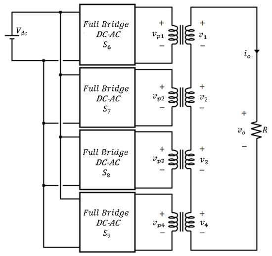
Figure 1.
Schematic diagram of the four-stage multilevel inverter based on a single-phase transformer.
The particularity of the asymmetrical configuration studied in this work is that the transformation ratios are not the same for each transformer, nor do they follow a geometric progression. The ratio (6:7:8:9) allows two main advantages: (1) a low harmonic distortion achieved with a signal of 31 levels (2.6 %) and (2) a balanced power distribution between the four DC-AC stages (25.61% : 25.24% : 24:70% : 24:45%) [6]. Although the concept developed in this paper can be extended to inverters with other asymmetric ratios, it is relevant to see that the redundancy provided by the ratio of 6:7:8:9 is a special case. In the previously mentioned work, for a normal operation of the inverter, redundancy is exploited to enforce balance in the power distribution among the inverter stages. In this new proposal, redundancy allows to provide alternative switching patterns to operate the inverter in a degraded mode when one of the stage goes out of service and maintain an acceptable quality.
To build the output signal depicted in blue color in Figure 2, the switches of the H-bridges of the inverter stages are commuted according to a switching pattern. Each level is held during a time interval in which we can define two time instants (firing angles), the time at which the interval starts and the time at which the interval ends. In consequence, the instant corresponding to the end of one interval is the same as the one in which the next interval starts. As a result of the symmetry of the produced signal, there are intervals with the same time duration. Considering the first quarter-cycle of the waveform in which the levels are increasing following a positive sequence (1, 2, 3…, M), it is possible to identify two sinusoidal envelopes, one above the square signal (external) and another below (internal). In the context of the work presented in this paper, if a pulse is aligned with the external envelope, it is considered that the pulse has outward alignment. Contrarily, if a pulse is aligned with the internal envelope, it is considered that the pulse has inward alignment. In Figure 2, the red color signal is the ideal sinusoidal reference to produce the output voltage.
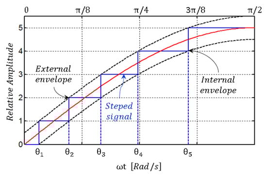
Figure 2.
A quarter of cycle of a multilevel signal showing relation of time intervals with external and internal envelopes.
The control of the inverter can be divided into two parts, one corresponding to operation in normal conditions and another corresponding to operation in faulty conditions. Integration of these two parts implies the implementation of a fault detection logic which provides information to the generator of the control signals of the H-bridges of the inverter and also to a complementary logic dedicated to imposing the isolation to the fault condition. Both the normal operation switching pattern and the faulty operation switching patterns are implemented by using lookup tables which are reproduced into a digital controller according to the fault detection logic. A block diagram containing the above described blocks for one of the stages of the inverter is shown in Figure 3. When a fault is detected, the isolation logic inhibits the control signals of the faulty stage and enforces a short circuit in the output using the same power semiconductors of the bridge or using an additional bidirectional switch connected at the output on the H-bridge. In a previous work, we proposed a method for the detection of inverter faults by means of machine learning techniques [22].
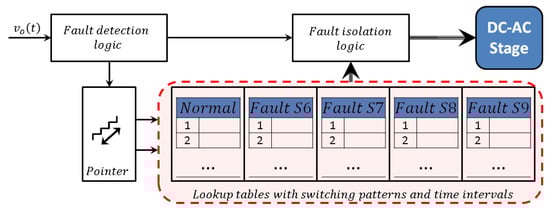
Figure 3.
Description of steeped signal along with external and internal envelopes.
3. Inverter Stage Failure Characterization
Given its operation, when a fault occurs in one of the inverter stages, the THD of the output voltage increases considerably, which can lead to an undesired increase in the circuit currents and deterioration of the components, among other inconveniences. Figure 4 shows the effect on the output signal in the presence of a fault due to an out-of-service failure of any of the inverter stages. For ease of graphical analysis, the output signal in the presence of a given fault is compared to an ideal sinusoidal signal with an amplitude value of 15. Please note that in the example, it is considered that one of the stages is in short circuit.
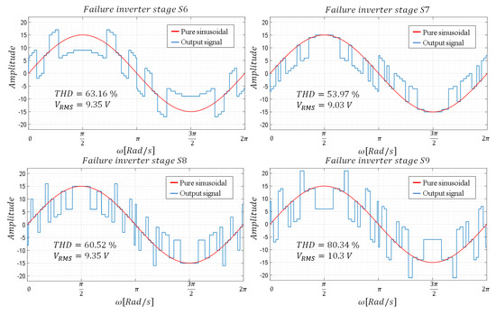
Figure 4.
Output waveforms for a failure in one of the inverter stages (short circuit).
As can be seen, the output signals present a clear deformation, modifying their effective voltage values, but above all, presenting a very high THD. Therefore, a new switching pattern is necessary to reconfigure the inverter when an anomaly is detected in the operation, thus reducing the THD to admissible levels. Table 1 presents the harmonic content of the output signal together with the THD, considering the presence of a short-circuit fault in one or two of the inverter stages.

Table 1.
THD, RMS voltage and amplitude of harmonic components for different inverter failures.
When one of the inverter stages fails, the system loses the ability to produce the full sequence of levels in the output signal. Table 2 shows the levels that can still be produced despite the failure of one of the stages. As can be seen, when the inverter stage fails, there are seven levels that cannot be produced (marked with X), when a failure occurs in the or stages, there are four levels that cannot be produced, and, when the inverter stage fails, there are five levels that cannot be produced.
Table 2.
Switching patterns to produce the output voltage levels in the event of a failure in one of the inverter stages.
4. Alternatives for Inverter Reconfiguration
To propose alternatives for the generation of the output signal in the absence of one of the stages, two reconfiguration methods are discussed below: One that uses pulses for the generation of each of the missing levels and one that produces a single pulse between the existing levels. For the first method, the use of one or two pulses and the alignment of these pulses in or out of the time interval of each of the missing levels is presented. For the second method, aligning the pulse in or out of the total time interval of consecutive levels and optimizing the THD based on the firing angles to reconstruct the missing levels are presented as variants.
4.1. Generation of Each Missing Level Using a Single Pulse
From what is presented in Table 2, an alternative is proposed to produce the missing levels based on the use of existing level pulses, considering that the level information is contained in the pulse duration. For example, when the inverter stage S6 fails (see cells with gray background color in Table 2), it is not possible to produce level 11. The realizable levels before and after are levels 10 and 15, respectively. Then, level 11 is replaced by a pulse between levels 10 and 15 with a duty cycle calculated by the following expression:
where Ni is the immediately preceding lower realizable level, Ns is the next higher realizable level, Na is the level to replicate, and D is the duty cycle to calculate. For the other levels in the same example (failure at inverter stage S6), the duty cycles are:
With the duty cycles obtained, two alternatives are proposed. The first one consists of aligning the pulse with the external part of the range of the level to be produced (outward alignment) and the second one aligning the pulse with the internal part of the range (inward alignment). As can be seen in Figure 5 and Figure 6, the inward alignment offers a lower THD in the signal obtained.
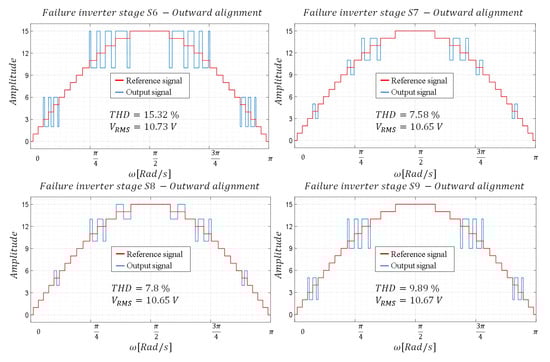
Figure 5.
Waveforms—Configuration with a pulse and outward alignment.
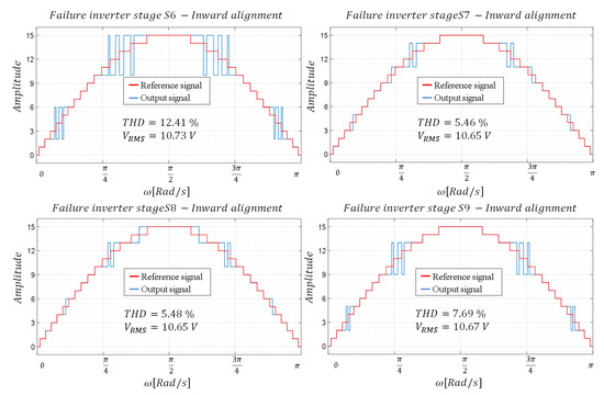
Figure 6.
Waveforms—Configuration with a pulse and inward alignment.
4.2. Generation of Each Missing Level Using Two Pulses
To produce the missing levels in the inverter using two pulses, the time interval corresponding to the desired level is divided into two equal time intervals, applying the same duty cycle determined for the one-pulse case to each of them. As in the case of a pulse, inward and outward alignment is considered to analyze its effect on THD. As can be seen in Figure 7 and Figure 8, similar to what happens in the case of a pulse, inward alignment favors a decrease in THD. A decrease in THD is also observed with respect to the case where only one pulse is used.
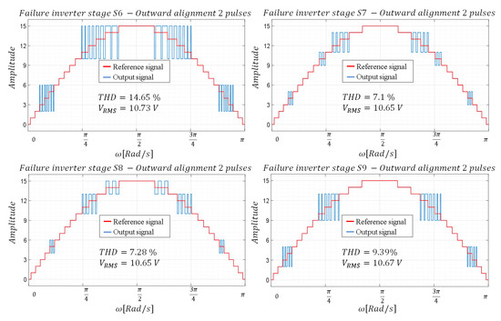
Figure 7.
Waveforms—configuration with two pulses and outward alignment.
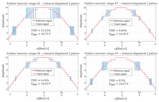
Figure 8.
Waveforms—configuration with two pulses and inward alignment.
4.3. Generation of Consecutive Missing Levels Using a Single Pulse
In this method, an equivalence is made between the areas of the missing levels and the area of a single pulse used to replace them. Hereafter, this alternative is referred to as the “base configuration”. Taking as an example the failure of the inverting stage , the consecutive levels 3, 4 and 5 are not reproducible, then, as represented in Figure 9, the areas corresponding to each of these levels are added to define the area of the pulse that will represent them in the signal.
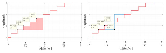
Figure 9.
Area of non-replicable levels (3, 4 and 5) with in failure.
The shadow zone in Figure 9 is defined as . The pulse used to replace the missing levels has an amplitude “h” (four levels in the example) and a base “b” calculated as indicated in Expression (2).
In this way, the duration of the pulse is obtained, which can be located from the beginning of the interval of the first consecutive non-realizable level or finish at the end of the interval of the last of the non-realizable levels. Following the aforementioned logic, the results shown in Figure 10 and Figure 11 are obtained.
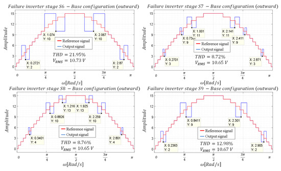
Figure 10.
Waveforms—Base configuration with outward alignment.
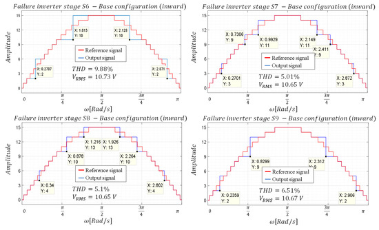
Figure 11.
Waveforms—Base configuration with inward alignment.
As can be seen when comparing Figure 10 and Figure 11, the inward aligned configuration is the most favourable for THD. However, it is not known whether the method used corresponds to the optimal one to obtain the lowest THD, so it is proposed to perform a complete sweep of the firing angles used to replace the missing consecutive levels. Consequently, each group of consecutive levels maintains a degree of freedom in the optimization. For example, in the case of a failure in inverter stage , there are two degrees of freedom, one corresponding to the angle to substitute levels 3 and 4, and another corresponding to the angle to substitute levels 11, 12 and 13. The range to perform the variation of the angles for the first interval (degree of freedom 1) is defined by the end angle of the interval producing the level two and the start angle of the interval producing the level five. Similarly, the range to perform the variation of the angles for the second interval (degree of freedom 2) is constrained between the ends of the interval corresponding to the level ten and the start angle corresponding to level 14. It is worth recalling that firing angles was computed following the procedure developed in [6]. All the degrees of freedom and the ranges of angles for the different inverter stages that fail are summarized in Table 3.
Table 3.
Degrees of freedom for optimization.
Considering the intervals presented in Table 3 and a resolution of 0.5°, a complete sweep of the angles is performed for each of the cases. To organize the results, Figure 12 shows the resulting THD as a function of the angle of one of the degrees of freedom.
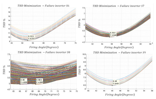
Figure 12.
Minimization of the THD for different failed inverter stages.
Table 4 presents the comparison of the THD obtained with the different methods, verifying that the optimization provided the best possible result. As can be seen, the most favorable THDs correspond to the failures of inverter stages and while the worst case corresponds to the failure of inverter . Figure 13 shows the waveforms obtained with the proposed optimization.
Table 4.
Comparison of THD (%) for different methods studied.
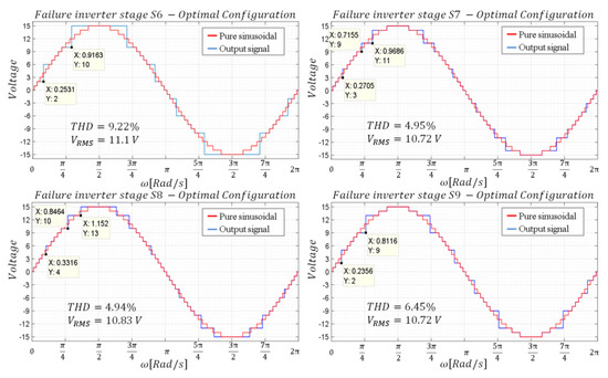
Figure 13.
Waveforms—Base configuration with optimization.
5. Simulation Results
To validate the results obtained for the best configuration, the simulation shown in Figure 14 was built using PSIM software. The simulation considers that the inverter has an input voltage of 48 V, produces an output voltage of 220 V and feeds an output load of 110 Ω. This implies that the isolation transformer of the inverter stages has the following turns ratios: 1:2.592725, 1:3.024846, 1:3.456966 and 1:3.889087. Power semiconductors and transformers are considered ideal (parasitic resistances are equal to zero). The step time of the simulation is defined as 0.9982 μs. The obtained signals are depicted in Figure 15.
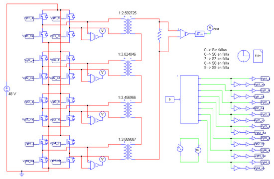
Figure 14.
PSIM simulation used to obtain validation results.
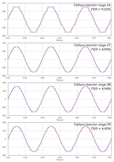
Figure 15.
Simulated results for possible failures in one of the inverter stages.
6. Conclusions
In this work, different methods have been developed to produce the output signal in the failure modes of the asymmetrical multilevel inverter with 6:7:8:9 ratio. Based on the results, it can be concluded that the use of a suitable firing angle to replace consecutive levels is more effective than the use of pulses with absent level information in the duty cycle. Results show that, in any failure case, the inverter would operate with an output voltage THD of less than 10 percent. Current work is devoted to the implementation of a laboratory prototype of the system integrating the detection, isolation and reconfiguration stages of the control. The corresponding results will be included in a subsequent publication.
Author Contributions
Conceptualization, O.L.-S.; Formal analysis, M.A.I.-O. and O.L.-S.; Investigation, M.A.I.-O., O.L.-S. and Y.A.A.-R.; Methodology, O.L.-S. and M.G.F.; Validation, M.A.I.-O. and O.L.-S.; Writing—original draft, M.A.I.-O., O.L.-S. and Y.A.A.-R.; Writing—review & editing, O.L.-S. and M.G.F. All authors have read and agreed to the published version of the manuscript.
Funding
This research received no external funding.
Data Availability Statement
The relevant data of this study have been included into the article. Additional information can be requested to the corresponding author.
Conflicts of Interest
The authors declare no conflict of interest.
References
- Rodriguez, J.; Lai, J.; Peng, F.Z. Multilevel inverters: A survey of topologies, controls, and applications. IEEE Trans. Ind. Electron. 2002, 49, 724–738. [Google Scholar] [CrossRef]
- Panda, A.; Suresh, Y. Performance of cascaded multilevel inverter by employing single and three-phase transformers. IET Power Electron. 2012, 5, 1694–1705. [Google Scholar] [CrossRef]
- Farakhor, A.; Reza Ahrabi, R.; Ardi, H.; Najafi Ravadanegh, S. Symmetric and asymmetric transformer based cascaded multilevel inverter with minimum number of components. IET Power Electron. 2015, 8, 1052–1060. [Google Scholar] [CrossRef]
- Barriuso, P.; Dixon, J.; Flores, P.; Moran, L. Fault-Tolerant Reconfiguration System for Asymmetric Multilevel Converters Using Bidirectional Power Switches. IEEE Trans. Ind. Electron. 2009, 56, 1300–1306. [Google Scholar] [CrossRef]
- Khomfoi, S.; Tolbert, L.M. Fault Diagnosis and Reconfiguration for Multilevel Inverter Drive Using AI-Based Techniques. IEEE Trans. Ind. Electron. 2007, 54, 2954–2968. [Google Scholar] [CrossRef]
- Lopez-Santos, O.; Jacanamejoy-Jamioy, C.A.; Salazar-D’Antonio, D.F.; Corredor-Ramirez, J.R.; Garcia, G.; Martinez-Salamero, L. A Single-Phase Transformer-Based Cascaded Asymmetric Multilevel Inverter with Balanced Power Distribution. IEEE Access 2019, 7, 98182–98196. [Google Scholar] [CrossRef]
- Sarwar, M.I.; Sarwar, A.; Farooqui, S.A.; Tariq, M.; Fahad, M.; Beig, A.R.; Alamri, B. A Hybrid Nearest Level Combined with PWM Control Strategy: Analysis and Implementation on Cascaded H-Bridge Multilevel Inverter and Its Fault Tolerant Topology. IEEE Access 2021, 9, 44266–44282. [Google Scholar] [CrossRef]
- Do, D.T.; Nguyen, M.K.; Quach, T.H.; Tran, V.T.; Blaabjerg, F.; Vilathgamuwa, D.M. A PWM Scheme for a Fault-Tolerant Three-Level Quasi-Switched Boost T-Type Inverter. IEEE J. Emerg. Sel. Top. Power Electron. 2020, 8, 3029–3040. [Google Scholar] [CrossRef]
- Amini, J.; Moallem, M. A Fault-Diagnosis and Fault-Tolerant Control Scheme for Flying Capacitor Multilevel Inverters. IEEE Trans. Ind. Electron. 2017, 64, 1818–1826. [Google Scholar] [CrossRef]
- Pires, V.F.; Foito, D.; Silva, J.F. Fault-Tolerant Multilevel Topology Based on Three-Phase H-Bridge Inverters for Open-End Winding Induction Motor Drives. IEEE Trans. Energy Convers. 2017, 32, 895–902. [Google Scholar] [CrossRef]
- Druant, J.; Vyncke, T.; De Belie, F.; Sergeant, P.; Melkebeek, J. Adding Inverter Fault Detection to Model-Based Predictive Control for Flying-Capacitor Inverters. IEEE Trans. Ind. Electron. 2015, 62, 2054–2063. [Google Scholar] [CrossRef]
- Chen, W.; Hotchkiss, E.; Bazzi, A. Reconfiguration of NPC multilevel inverters to mitigate short circuit faults using back-to-back switches. CPSS Trans. Power Electron. Appl. 2018, 3, 46–55. [Google Scholar] [CrossRef]
- Reddy, B.P.; Rao A, M.; Sahoo, M.; Keerthipati, S. A Fault-Tolerant Multilevel Inverter for Improving the Performance of a Pole–Phase Modulated Nine-Phase Induction Motor Drive. IEEE Trans. Ind. Electron. 2018, 65, 1107–1116. [Google Scholar] [CrossRef]
- Kim, S.M.; Lee, J.S.; Lee, K.B. A Modified Level-Shifted PWM Strategy for Fault-Tolerant Cascaded Multilevel Inverters with Improved Power Distribution. IEEE Trans. Ind. Electron. 2016, 63, 7264–7274. [Google Scholar] [CrossRef]
- Zhou, L.; Smedley, K.M. Postfault Control Strategy for the Hexagram Inverter Motor Drive. IEEE Trans. Ind. Electron. 2010, 57, 2719–2729. [Google Scholar] [CrossRef]
- Zhao, W.; Chen, Z.; Xu, D.; Ji, J.; Zhao, P. Unity Power Factor Fault-Tolerant Control of Linear Permanent-Magnet Vernier Motor Fed by a Floating Bridge Multilevel Inverter with Switch Fault. IEEE Trans. Ind. Electron. 2018, 65, 9113–9123. [Google Scholar] [CrossRef]
- Nguyen, L.V.; Tran, H.D.; Johnson, T.T. Virtual Prototyping for Distributed Control of a Fault-Tolerant Modular Multilevel Inverter for Photovoltaics. IEEE Trans. Energy Convers. 2014, 29, 841–850. [Google Scholar] [CrossRef]
- Aleenejad, M.; Mahmoudi, H.; Ahmadi, R. Multifault Tolerance Strategy for Three-Phase Multilevel Converters Based on a Half-Wave Symmetrical Selective Harmonic Elimination Technique. IEEE Trans. Power Electron. 2017, 32, 7980–7989. [Google Scholar] [CrossRef]
- Ouni, S.; Zolghadri, M.R.; Khodabandeh, M.; Shahbazi, M.; Rodriguez, J.; Oraee, H.; Lezana, P.; Schmeisser, A.U. Improvement of Post-Fault Performance of a Cascaded H-bridge Multilevel Inverter. IEEE Trans. Ind. Electron. 2017, 64, 2779–2788. [Google Scholar] [CrossRef]
- Biberoğlu, M.; İnce, K.; Karaosmanoğlu, F. Design of fault-tolerant cascaded H-Bridge multilevel inverter with output-side transformers using bidirectional switches. In Proceedings of the 2015 International Conference on Renewable Energy Research and Applications (ICRERA), Palermo, Italy, 22–25 November 2015; pp. 98–103. [Google Scholar] [CrossRef]
- Dixon, J.; Barriuso, P.; Ortuzar, M.; Moran, L.; Pontt, J.; Rodriguez, J. Fault tolerant reconfiguration system for asymmetric multilevel converters using bi-directional power switches. In Proceedings of the IECON 2007—33rd Annual Conference of the IEEE Industrial Electronics Society, Taipei, Taiwan, 5–8 November 2007; pp. 2124–2129. [Google Scholar] [CrossRef]
- Salazar-Dantonio, D.; Meneses-Casas, N.; Forero, M.G.; López-Santos, O. Automatic fault detection in a cascaded transformer multilevel inverter using pattern recognition techniques. In Iberian Conference on Pattern Recognition and Image Analysis; Springer: Cham, Switzerland, 2016; pp. 378–385. [Google Scholar] [CrossRef]
Publisher’s Note: MDPI stays neutral with regard to jurisdictional claims in published maps and institutional affiliations. |
© 2022 by the authors. Licensee MDPI, Basel, Switzerland. This article is an open access article distributed under the terms and conditions of the Creative Commons Attribution (CC BY) license (https://creativecommons.org/licenses/by/4.0/).