Article

Methods of Deployment and Evaluation of FPGA as a Service Under Conditions of Changing Requirements and Environments

by
Artem Perepelitsyn
* and
Vitaliy Kulanov
Department of Computer Systems, Networks and Cybersecurity, National Aerospace University “KhAI”, 17, Chkalov Str., 61070 Kharkov, Ukraine
*
Author to whom correspondence should be addressed.
Technologies 2025, 13(7), 266; https://doi.org/10.3390/technologies13070266
Submission received: 27 March 2025 / Revised: 26 April 2025 / Accepted: 29 April 2025 / Published: 23 June 2025

Abstract

Applying Field Programmable Gate Array (FPGA) technology in cloud infrastructure and heterogeneous computations is of great interest today. FPGA as a Service assumes that the programmable logic device (PLD) is used as a remote (available over the Internet) service with an FPGA silicon chip on board. During the prototyping of FPGA-based projects within modern design flow, it is necessary to consider the processing delays caused by various factors, including the delay of data transfer between the kernel and host computer, limited clock frequency, and multiple parallel-running FPGA accelerator cards. To address these challenges, three techniques are proposed to reduce the required modification efforts and improve project performance. Based on the proposed models, the analytical evaluation of the functioning process of FPGA as a Service is performed to determine possibilities of improving productivity and reducing the response time. The practical experience of porting FPGA projects to new integrated environments is considered. The evaluation of the response time of FPGA as a Service using the queueing theory is proposed. It is shown that scaling and parallelization at the top level of project hierarchy, pipelining, and parameterization allow for the effective deployment of such FPGA systems for data centers and cloud infrastructures. The proposed techniques and models allow for an evaluation of the performance and response time of FPGA as a Service for formulating recommendations to improve technical characteristics.

1. Introduction

In today’s rapidly evolving technological landscape, the importance of scientific advancements and technological innovations in engineering cannot be overstated. The transition toward new solutions in projects built on the programmable logic device platform directly impacts numerous critical application domains [1,2].
Recent changes in FPGA technology have significantly improved their performance, flexibility, and power efficiency [3]. Key advancements in the FPGA market include enhanced design tools, like Vivado and Quartus Prime, which simplify the creation of complex designs and enable the development of System on Chip (SoC) and System on Programmable Chip (SoPC) solutions [4].
Next-generation FPGA architectures, incorporating 3D transistors and Silicon on Insulator (SOI) technology, improve performance by increasing bandwidth and reducing power consumption [5].
Advanced routing algorithms and optimization techniques allow precise latency prediction, ensuring critical systems consistently meet performance requirements [6]. Low-power technologies, such as FinFETs and neuromorphic cores, have significantly reduced power consumption while maintaining high performance [7].
Recent improvements have also integrated robust security features directly into FPGA architectures, enabling secure cryptographic functions and data processing capabilities essential for safety-critical applications where data integrity and protection against malicious attacks are vital [8]. Modern optical interfaces on such FPGA accelerator cards significantly improve network capabilities [9] and the performance of image processing using neural network implementation.
Introducing new paradigms, approaches, and architectures is crucial for effectively addressing challenges associated with prototyping complex FPGA-based safety-critical systems and components [10,11].
Changes in requirements during the product lifecycle and short time to market necessitate continuous improvement in technical approaches and flexibility in responding to evolving needs. Nowadays, developing new projects may consume a timeframe comparable to the lifespan of the products they are intended to serve [12]. It is crucial to conduct a thorough evaluation when selecting manufacturers, toolchains, and hardware platforms. This decision is essential, as investments in projects built around a specific hardware–software platform may face the risk of obsolescence within just a few years.
Also, a manufacturer may discontinue support for a previously prevalent family of chips [13,14] or software tools [15], replacing them with a newer [16], more advanced generation and, as a result, significantly influence the project’s infrastructure or architecture through functional constraints or other technology-related factors. Additionally, companies producing programmable logic silicon chips often find it exceedingly challenging to support multiple toolchains concurrently [17,18]. Sometimes, their policy imposes restrictions on the involvement of legacy versions of their tools [19].
An alternative approach for designing FPGA-based projects is to apply the FPGA as a Service paradigm, wherein access to hardware platforms is provided through cloud service providers [20]. This strategy allows developers to create projects without incurring substantial costs for procurement and maintenance of physical hardware. Engineers can lease FPGA resources [21] on demand and scale them [22] according to project requirements. This methodology also mitigates the vendor lock-in problem [23], enabling access to the latest FPGA silicon chip families in a cloud environment.
Utilizing FPGA as a Service can be particularly advantageous when rapid prototyping and the capacity to scale a project are critical success factors. Among the core benefits is access to high-performance computing resources without expensive on-premises self-maintained infrastructure or specialized hardware. It is also the way to achieve redundancy and fault tolerance by harnessing the capabilities of cloud services, including storage and analytics.
Recent industry trends force the growing momentum of FPGA adoption in cloud-based and adaptive computing environments. For example, AMD’s Versal AI Core series exemplifies a shift toward adaptative SoCs that integrate artificial intelligence (AI) engines, digital signal processing (DSP), and programmable logic to support heterogeneous workloads with low latency [24].
In the cloud domain, AWS EC2 F1 instances, Microsoft Azure’s NP-series VMs, and Alibaba Cloud [12] highlight the practical deployment of FPGAs at scale, allowing developers to accelerate ad hoc workloads. Amazon Web Services provides FPGA resources within Amazon EC2 F1 that are used for various tasks, including big data processing and machine learning using the possibility of creating of own FPGA hardware accelerators with VHDL and Verilog languages.
Microsoft Azure also offers FPGA acceleration through the Azure FPGA Platform for large-scale computing and intensive computing as a part of scientific research with the support of various frameworks, including Intel oneAPI Toolkits and OpenCL [12].
Alibaba Cloud offers FPGA acceleration through the FPGA Elastic Compute Service that is widely used to develop and deploy solutions for artificial intelligence, finance, and other industries with the use of its own tools for prototyping projects.
While such efforts demonstrate the scalability of FPGA resources, challenges remain in ensuring efficient dynamic resource allocation and maintaining quality of service (QoS) to meet changing system requirements.
When managing remote operations with FPGA boards, it is crucial to consider shared access, which involves configuring permissions and establishing an organized queue system [20,25].
This model ensures QoS by adhering to critical performance metrics, including response time, to evaluate the risks. To initiate interaction with FPGA as a Service, clients request to lease dedicated resources such as FPGA boards, RAM, CPU cores, and corresponding software applications and tools. Provisioning FPGA as a Service enables users to create a host machine equipped with connected FPGA boards. These devices can be accessed remotely using various interfaces, such as Peripheral Component Interconnect Express (PCIe) [26].
Service-oriented software is utilized along with an integrated system for processing and control processes for data loading and firmware configuration to set up programmable logic [20,27]. Developers interact with the server for data sharing and collection. They can provide a bitstream configuration file (software) for the programmable device.
But the specifics of the continuous updating of versions of communication framework involved in service creation, as well as compatibility problems between versions of software tools for the creation of projects, and the drop of performance of systems in newer versions of integrated environment require a comprehensive methodological solution.
The goal of this study is to improve engineering experience in developing FPGA-based projects by enhancing existing methods, technologies, and tools for deploying and evaluating FPGA as a Service.
To achieve this goal, it is necessary to perform the following tasks:
1.
to analyze the history of product changes of the leading vendors and manufacturers of programmable logic devices;
2.
to conduct a comparative analysis of modern development FPGA boards and accelerator cards;
3.
to analyze the dynamics of changes in the functionality of integrated environments for FPGA-based systems considering the existing requirements and restrictions of different versions of software and hardware platforms and components;
4.
to propose the techniques for the creation and optimization of high-performance systems based on FPGA that are tolerant to project requirement changes;
5.
to analyze the delays in communications between the host computer and FPGA kernels;
6.
to propose the technique for evaluation and reduce the response time delay for FPGA as a Service, depending on the number of involved resources (FPGA cards).
The article is organized as follows. Section 2 analyzes challenges arising from changing requirements and integrated environments. Section 3 details techniques for creating and optimizing FPGA as a Service. Section 4 proposes models for evaluating QoS and a technique for reducing delays of FPGA as a Service. Section 5 and Section 6 discuss the results and conclude this study correspondingly.

2. Analysis of Technology Stack for the Creation of FPGA as a Service

2.1. Evolution and Competitive Landscape of PLD Manufactures

Among the foremost manufacturers of programmable logic devices, four prominent companies can be underscored: Intel, AMD (Xilinx), Microsemi, and Lattice Semiconductor. Lattice and Microsemi are specialized in fabricating silicon chips that can be programmed for various applications. These firms provide straightforward solutions, enabling a comprehensive analysis of their microcircuits for embedded devices and identifying defects.
These products are utilized in constructing critical systems globally, with their functional capabilities facilitating robust project implementation. The software tools supplied by these manufacturers exhibit certain limitations in their functionalities. Nevertheless, they remain adequate for modern project creation and bear many resemblances to the tools offered by leading companies with over three decades of experience.
Xilinx and Altera are two companies that may be deemed flagships within the industry. The competition between the two giants of microelectronics (Intel and AMD) continues to extend into the realm of programmable logic chip manufacturing. AMD produces Xilinx families [21], while Intel previously acquired Altera, which now operates under the new brand Intel-Altera. The emergence of new types of processors, including the M1, which is based on ARM architecture, also reflects the dynamism in the semiconductor market. This architecture is utilized in FPGAs as a processing core, providing a balance between performance and low power consumption for embedded solutions. The presence of competition catalyzes price reduction and can accelerate the implementation of new ideas. This research primarily focuses on the products of Xilinx, as the programmable solutions from Intel-Altera have already been analyzed in previous studies.
In addition to Intel and AMD (Xilinx), smaller yet innovative companies are carving out their niche in the programmable logic industry. Companies like Achronix and Efinix have introduced unique FPGA architectures tailored for specific high-performance and low-power applications. Achronix, for instance, focuses on high-speed data processing with its Speedster line of FPGAs, while Efinix emphasizes efficiency and adaptability for edge computing scenarios. These emerging players bring fresh perspectives to the market, often targeting specialized applications that may not align with the broad product strategies of larger competitors. Their contributions diversify the ecosystem and stimulate innovation, challenging established FPGA design and functionality standards.
Building an FPGA as a Service necessitates strategically integrating the diverse offerings and competitive advantages presented by major manufacturers with the innovative solutions of emerging players in the field. FPGA as a Service is positioned to meet users’ evolving and expanding needs across various sectors by addressing various applications and providing cost-effective services.

2.2. Analysis of Capabilities of Modern FPGA Silicon Chips and Cards

Modern FPGA accelerator cards have emerged as reconfigurable platforms for various applications. Developers can implement their projects by configuring the parameterized architecture of existing FPGA cores according to specific requirements, which often results in higher performance than products with predefined architectures [20,22].
The increasing demand for higher data exchange speeds between system components has expedited the transition to High Bandwidth Memory (HBM) technology. This trend facilitates the consolidation of various bridges and substrates within the chip, enabling microchip integration into a single package. As a result, this integration contributes significantly to reductions in energy consumption and performance improvements. HBM technology includes multiple versions, including HBM2e. The company Hynix has initiated the production of ultra-fast HBM2e dynamic memory chips. Within a single silicon chip of 16 GB memory, the bandwidth can reach up to 460 gigabytes per second [21]. Achieving such speeds is often unattainable in many practical implementations, as they are calculated based on interface capacity. In linear read mode, achievable speeds may reach 400 gigabytes per second, while random read conditions may yield about 260 to 280 gigabytes per second. The core of these development kit boards is an FPGA chip from the UltraScale category, which offers a substantial array of resources at a high financial cost. An alternative option involves the utilization of engineering sample (ES) models, which allow operational access to the board before it enters the market. However, this approach does not guarantee that the final version will use the same components, and ongoing support for firmware remains an open issue.
In response to market conditions, developers are exploring ways to cut production costs, which could lead to lower prices for development boards. One strategy involves creating products that function similarly to flagship models, incorporating specific hardware optimizations that might compromise performance up to three times in some situations and by 1.5 times in others.
This means that such boards may operate at just a quarter of their full productivity potential. The performance can be boosted by implementing active cooling solutions, significantly raising output without adding extra costs. As a result of corporate policies, many boards soon lose support despite having extensive hardware capabilities and being widely adopted and often costly. These products may receive no further support from development tools; for example, an earlier version of an integration development environment might not allow project compilation at a specified clock frequency for a specific board. A newer version might permit this but could drop support for that board, even while the core functionality has stayed the same. Consequently, these boards frequently struggle to achieve mass adoption and are typically used only during prototyping phases.
Analyzing changes in development environments entails reviewing the historical evolution of these tools from their inception to the present day. Investigation of data center and development board technologies for creating data processing systems, including FPGA as a Service, reveals a state of continuous transformation [20].
Currently, numerous alternatives to FPGA boards exist. One notable example is the VCU1525, a powerful board without HBM designed for various classical processing tasks, such as video conversion. Other boards, like U200 and U250, have been introduced, allowing integration with expandable DDR4 memory. U25 is a card for network tasks.
U50 [21] and U280 [28] are cards with 8 GB of HBM. U55C is one of the most powerful FPGA accelerator cards with 16 GB of HBM [29]. However, the disadvantage of this U55C card is that the number of independent memory channels that connect the project to the exact memory block is the same as that in U280 and U50. The VHK158 board also contains HBM2E memory of 32 GB, but this evaluation kit is designed for machine learning and implemented in another form [30]. The UL3524 [31] accelerator card is designed without HBM and is targeted at implementing custom algorithms and artificial intelligence-enabled trading strategies.
AMD and Alveo provide various FPGA accelerator cards with different resources. They can be grouped in a chassis [32] to mount in data centers with proper centralized cooling. One host machine can contain many slots for cards. They can be programmed independently or as a single dedicated “task”. These boards are typically designed as standard (PCIe) extensions, often including additional power supplies, active cooling, and supplementary external communication interfaces. Simpler implementation alternatives are also available, serving as cost-effective options by minimizing additional hardware peripherals and resources (e.g., available memory volume, type of user/host system interaction interface).

2.3. Analysis of Software Platforms and Designing Tools

The first toolset from Xilinx for handling the entire design flow, including Vivado, was the SDAccel design environment [33]. Such integration simplifies the interaction between designers and the input/output configurations of FPGA chips while expanding the supported methods for project descriptions.
This automation entails the presence of an embedded firmware module within each project. This immutable firmware, the shell, facilitates data transfer from the host application on the computer to the user-defined modules within the FPGA over the PCI Express interface.
Within the standard development process using SDAccel, an iterative loading of the required pre-compiled configuration into the FPGA is anticipated in the form of a completed kernel or a collection of kernels. From the perspective of a host application written in C or C++, interaction with the kernel appears as a function call that includes the passing of parameters.
If the kernel embodies an OpenCL solution, its syntax on the FPGA side closely resembles that of a function in a programming language. In contrast, if the kernel is described using register transfer level (RTL) in Verilog, System Verilog, or VHDL, the set of blocks for supporting the standard bus for connection of modules inside FPGA projects known with the name Advanced eXtensible Interface (AXI) must be integrated into the project to enable interaction with the Xilinx Runtime (XRT) framework [34]. This specific characteristic opens significant potential for utilizing the entire suite of described solutions to provide FPGA as a Service using XRT-managed (or controlled) kernels.
The development process with this toolkit has several key features, such as describing both the host application and the FPGA project within one cohesive environment, and variations of implementation efficiency across C, C++, OpenCL, VHDL, Verilog, and System Verilog. The operation is confined to specific Linux versions, including Ubuntu, within an environment that disallows updates. Windows is generally unsupported. Also, there are many undocumented and yet-to-be-explored issues that impede a standard development process [23].
Such applications consist of a host component and a kernel for deployment in FPGAs. FPGA boards and system emulation on a processor during development can be utilized. If the project is implemented in OpenCL, C, or C++, the potential exists for high-speed software simulation of the system’s operation. Practical experience with SDAccel tools and rapid prototyping methodologies indicates that implementing a complex computational system based on FPGAs has become a routine engineering task.
The capability for high-speed data exchange with FPGA boards not only ensures high throughput during system operation but also significantly enhances the effectiveness of testing processes throughout the product’s lifecycle. Complex implementations can utilize actual datasets, often measured in gigabytes, as test cases, which helps validate the system’s performance and robustness under realistic operating conditions.
One of the primary objectives for developers is to reduce labor-intensive costs during the product design phase. The vast majority strive to achieve this goal, so the available tools and strategies are enormous. Among these strategies is incorporating “redundant” resources, which can be made possible by increasing the available memory for development tools. Such enhancements significantly lessen the complexity of the development process for engineers, demonstrating an overarching trend in development environments toward greater automation in project creation.
Xilinx invested considerable time in its ISE development environment at various stages of its evolution. In contrast, during the same period, Altera’s popular solution was the Quartus II development environment, which, even after rebranding, retained the same name in Intel’s product lineup. Xilinx ultimately phased out ISE in 2014.
Since then, it has been succeeded by the Vivado design environment, which later became part of a portfolio of more robust products [35]. The Vivado environment facilitates the synthesis of design solutions, allowing the integration of traditional FPGA design processes with more advanced high-level entities.
These include programming languages such as C and C++, OpenCL, and support for other technologies that meet contemporary automation demands. From 2016 to 2018, the market also featured the SDx package, which included SDAccel. This powerful solution for programming FPGA-based programmable logic leverages all its advantages, incorporating a new programming paradigm of runtime reprogramming of FPGA using the XRT framework.
The relationships among integrated environments during their transition reveal that multiple development environments can coexist simultaneously, yet projects do not remain compatible (Figure 1).
Along with the development of the SDAccel environment, Xilinx spent five years creating the Vitis development environment [36], which incorporates most features, including SoPC functionalities, platforms for artificial intelligence development, and support for various programming languages that are transformed into RTL descriptions for programming FPGAs [22]. After the preparation and release of the Vitis environment, support for the SDAccel development environment and compatible development packages was discontinued. This swift transition to new development environments necessitated the adaptation of all existing projects, indicating the need for preparation for subsequent changes.
Despite the promised integration of Git and support for version control systems, both environments have been found lacking, according to Xilinx’s technical support. While SDAccel and Vitis theoretically offer such tools, they need to function more effectively in practice. Transitioning projects between these two development environments is only possible by completely recreating them step by step. There is no capability for export and import that would allow a project to be compiled afterward.
Despite the external differences being minimal (with similar graphical interfaces), the manufacturer claims backward compatibility, which, in practice, does not hold up. The lack of true backward compatibility significantly complicates the maintenance of existing projects. Therefore, considering the dynamic changes in the design environments, developing a clear strategy for managing the development and project support process is essential. This requires continuous monitoring of existing solutions to ensure readiness for possible modifications.
Another product from Xilinx is the Xilinx Runtime framework [34]. XRT facilitates communication with FPGAs and direct programming. This is a significant part of the Vitis design flow and the key element for XRT-managed kernels. Namely, the use of XRT simplifies for engineers the process of the creation of FPGA as a Service. This framework serves as an interface between FPGA solutions in PCIe accelerator card format and host solutions based exclusively on specific versions of Ubuntu or CentOS operating systems.
The Vitis development environment does not assume the possibility of working with Windows, but its components, including Vivado, still allow such use. This framework monitors all processes associated with the FPGA board, including temperature monitoring and access control (firewall). Its primary function pertains to data exchange operations and runtime reprogramming, which shifts the focus away from traditional FPGA systems.
With runtime reprogramming, the most complex FPGA accelerator can be represented as a C-like language function invoked directly from a running host application. The entire system’s interaction is encapsulated in a single line of code where parameters are passed. For the programmer, interacting with the FPGA becomes a simple function call, followed by waiting for a readiness flag for the processed data and the ability to read it from buffers.
This mode of interaction is convenient. However, a correct understanding of the FPGA’s role within such a system is required. XRT allows for near-instantaneous programming. Preparing a set of pre-compiled IP cores (directly prepared binary files of the necessary projects for FPGA loading) is recommended for runtime reprogramming. These cores can be specified as parameters in the host program and invoked in any sequence almost instantaneously. The execution duration of instructions on each IP core depends on the tasks being addressed, closely aligning with the familiar paradigm of FPGA operation. It is worth mentioning that the characteristics of PCIe interaction limit the execution of cores to just a few seconds. Therefore, data processing should be conducted in batches.
Transitioning to development using these new development environments necessitates a paradigm shift in how developers perceive the role of FPGAs within the designed system. For many experienced developers, this transition from consideration of the FPGA system as the center of prototyping to just a function can be unexpectedly challenging.
Having spent years honing their expertise using traditional approaches, these developers may have developed ingrained habits and workflows that are difficult to alter. New environments often introduce different methodologies, programming languages, and conceptual frameworks that require developers to expand their skill sets and embrace a broader perspective on system architecture.
But, the XRT framework is also developing in parallel with integrated environments and demonstrates similar compatibility problems involving FPGA solutions from the releases of different versions.
For each supported version of the operating system and for each modification of the integrated environment, a specific version of XRT is created [37]. This software component must be installed considering the version of Vitis and the version of the shell firmware in a target Alveo FPGA card. There is a strong correlation between the supported versions of XRT for each version of a board shell [38].
Updating firmware for such FPGA accelerator cards is a complicated procedure that requires access to each board with a power cycle. This procedure cannot be performed remotely or in the data center without access.
Furthermore, each FPGA board has a limited number of supported XRT versions. For example, for Alveo U280-ES1, there are only two supported XRT versions. At the same time, only one installed version of XRT is allowed at a time in the operating system. It makes parallel work on the same computer with FPGA accelerator cards with different shell versions impossible, even within virtual machines or dockers, as well as the development of projects installed in parallel with different Vitis versions. These compatibility problems must be taken into account during the maintaining of projects.

3. Method of Deployment of FPGA as a Service

3.1. Steps for FPGA Project Development Within FPGA as a Service Flow

Based on the analysis, measures can be proposed to facilitate prototyping and support of long-term projects. These measures should be accompanied by explicit guidance for FPGA as a Service developers who utilize tools from prominent manufacturers.
Formulating these solutions based on the following recommendations is imperative. Adhere to best practices to ensure that the implementation of the FPGA project is independent of the specifics of any development tool (vendor lock-in).
This principle will facilitate future modifications and transitions across various tools and third-party libraries. Then, prepare a plan to design generic parts of a system to ensure the potential for changes within the components and the ability to port these solutions (simplified porting) to updated and modified development environments. Designing with flexibility in mind will enhance the systems’ durability and adaptability. Use command-line interface (CLI) to organize project maintenance processes without relying on the development environment’s graphical user interface (GUI). Instead, leverage command-line interface that ensure backward compatibility among various development tools and environments.
This approach can streamline project handling and reduce dependencies on graphical aspects that may change over time. Maintain continuous feedback mechanisms to establish a constant feedback loop with IDE developers and resolve issues related to compatibility between current and upcoming tool releases. This proactive communication ensures that developers can obtain insights about new commands or updates in the tools before they are publicly available in specifications or incorporated into newly released development environments.

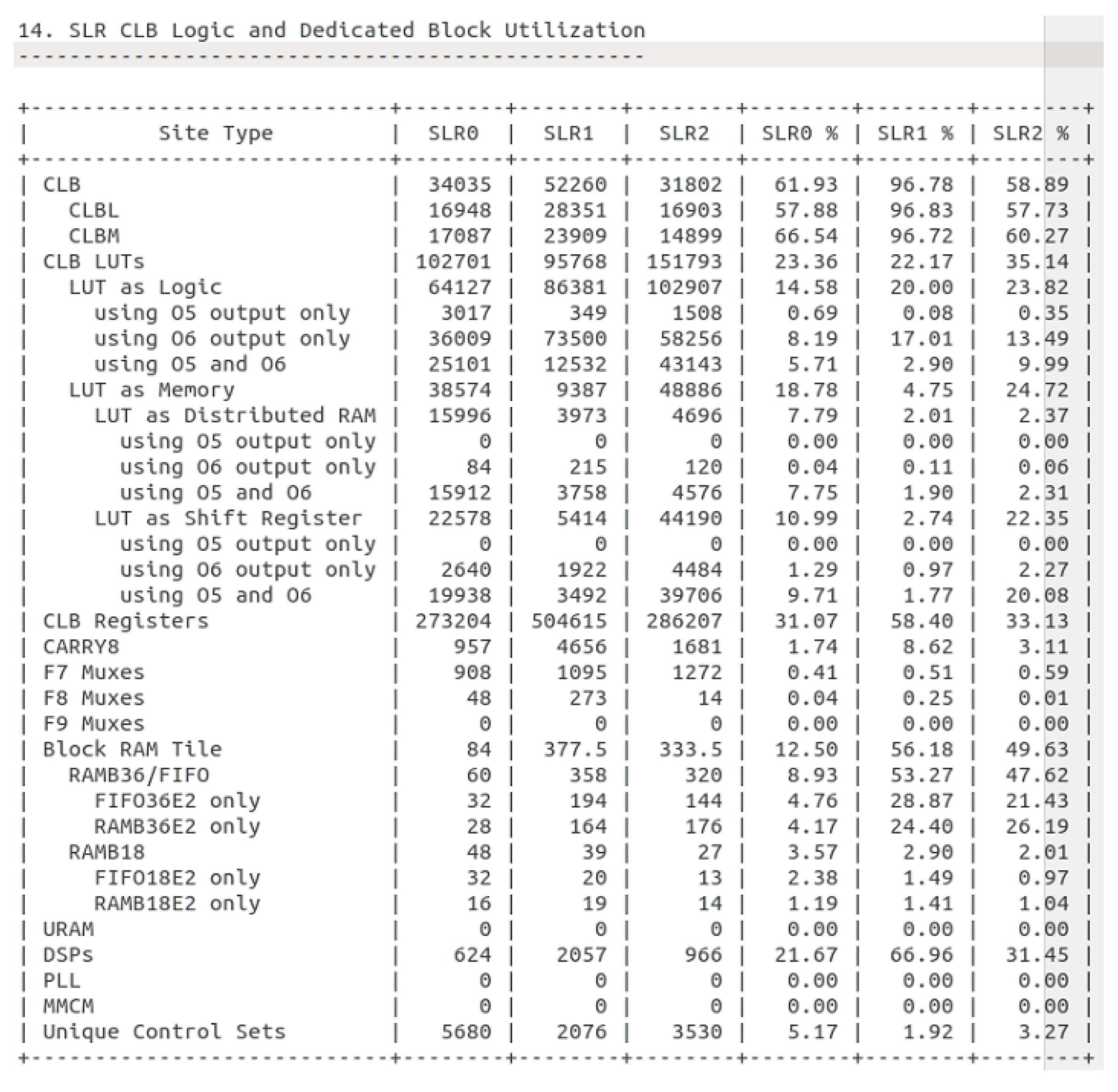
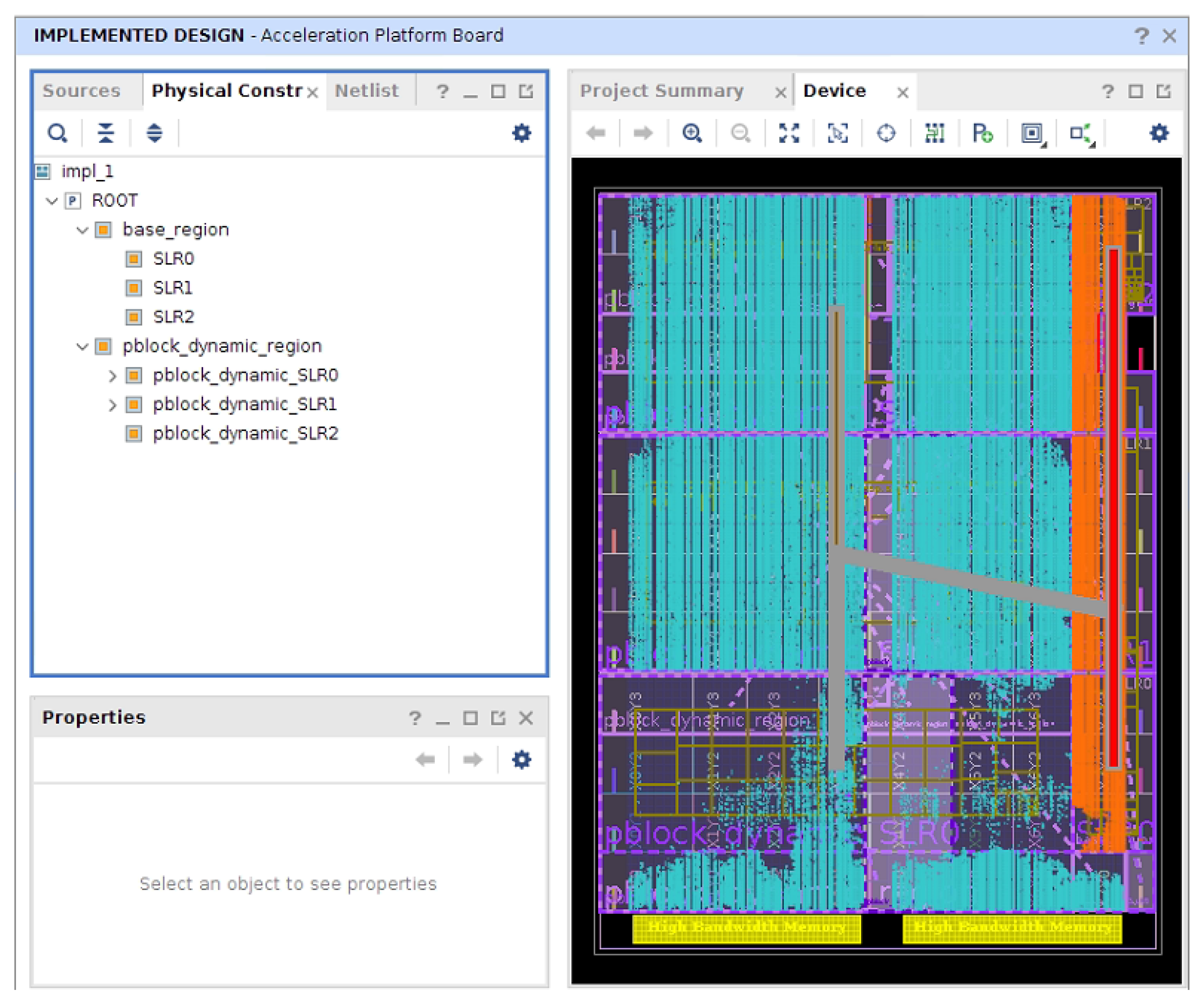
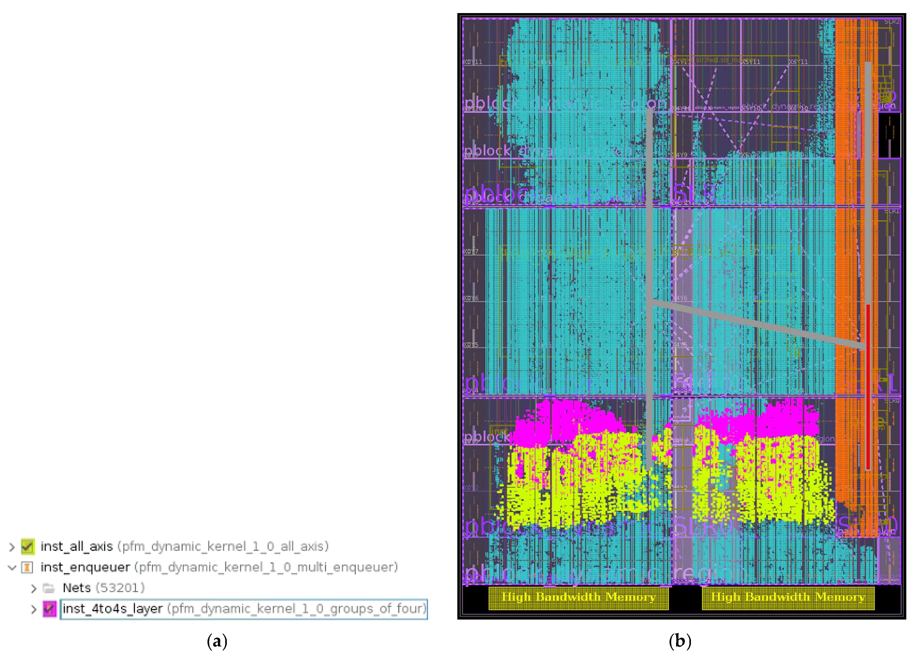
3.2. SLR Placement Optimization Strategy

FPGA projects during the Place&Route phase have a challenge related to associating resources with specific regions of the chip [39], referred to as Super Logic Regions (SLRs). Think of SLRs as “neighborhoods” on the FPGA chip—placing critical modules in the right neighborhood reduces “commute time” for signals, boosting overall efficiency. These regions contain a fixed set of interconnections [40], which allows for binding certain implementations to specific SLRs based on project requirements [35]. For instance, one development environment version enables binding distinct project components to regions on the SLR chip.
However, this functionality may be present in one FPGA but absent in another, even though both are of the same board version. The fundamental reason for this discrepancy is that one of the boards is an “engineering sample”, while the other is a standard mass-produced unit.
Since the primary project is developed on an engineering version, transitioning it to the main board allows for long-term support and the ability to bind specific sections or elements of a region to parts of the chip. However, the limitations of using the tool during the design stage often hinder this capability, necessitating redesign efforts for optimization solutions.
Considering these constraints, the following strategy can be proposed to enhance performance and simplify routing for FPGA as a Service. Implementing node splitting along with a selection of registers, as advised by the manufacturer, will enhance the trace routing of these solutions using the available tools. Incorporating a set of two or three sequentially connected buffers facilitates data processing through their utilization of pipelining.
Adding a tag to the data being processed, which can be represented as a link between a unique identifier and the dataset, based on a compact representation of this data using several bits in the case of processing large data arrays, significantly simplifies the process of pipelining and allows full binding and association of data with a unique identifier. Finally, map the project modules and their parts by moving the most reasonable blocks on the chip to another SLR. This approach facilitates the synchronization of processed data at the final processing nodes with the addition of an arbitrary number of intermediary steps in the form of a set of registers, which can simplify the routing process for such solutions to achieve the desired frequency and thus enhance performance while streamlining routing.
Adhering to these recommendations can reduce compilation time for such projects on the one hand and increase the chances of achieving the desired final frequency upon compilation on the other hand.
Furthermore, it is essential to highlight the ability to limit the number of concurrently processed projects within a single dataset to reduce the dimensionality of individual solutions due to the limited number of input and output physical connection lines within individual SLR regions. Following these recommendations may lower labor costs when transferring a project to new boards or new FPGA cards without incurring additional expenses for modifying such projects. Sometimes, the requirements of integrated environments and target boards change, leading to clarifications in client specifications.

3.3. Application of Proposed Techniques for FPGA as a Service

The research results were applied in designing an image processing service utilizing Alveo U280 FPGA accelerator cards within the SDAccel 2018 development environment. Subsequently, the project was migrated to the Vitis 2019 development environment and then to Vitis 2020. All three environments are incompatible, and a typical migration requires a step-by-step redesign of all project components and compiler parameter adjustments. The project was then migrated to Vitis 2021 and Vitis 2022 accordingly.
Changes in the development environment can significantly impact the ability to implement individual elements, potentially altering their functionality and integration within the overall system. Such variations may arise due to differences in available tools, compatibility issues, or updates in software frameworks, necessitating careful consideration and adjustments to maintain optimal performance.
For example, if specific boards allowed for a parallel bus width of 2048 bits, on another board, the inability to transfer such solutions from one SLR area to another necessitated either changing the number of modules that would process data in parallel to free up a certain number of communications lines or reducing the bus width to 1024 or 512 bits. This change in project requirements can arise from alterations in the development environment or the target chip.
The FPGA project’s performance depends on the kernel’s resulting frequency after compilation. Moving to newer versions of XRT frameworks associated with the new Vitis version requires the new shell version for FPGA accelerator cards [37,38]. Each version adds the number of commands for transferring static kernel parameters over the AXI bus, making the additional components of the static region more complicated from version to version. If an existing project consumes many chip resources, any extra components can turn it into a borderline state and reduce the final frequency or placement problems. In this case, the iterative process of selecting the specified frequency parameters makes it possible to obtain a higher final frequency while parameter -O02 is specified (Figure 2).
To improve the probability of project placement with the desired final frequency specified with --kernel_frequency for each clock source, the additional parameters vivado_prop can be added to the v++ chain (Listing 1). These parameters force Vivado to make multiple placement attempts with additional strategies. They can significantly increase the duration of the entire compilation process in Vitis, especially with compiler parameters -O02 and -O03. Avoiding generating the project cache with the parameter --no_ip_cache can save up to a quarter of the compilation time.
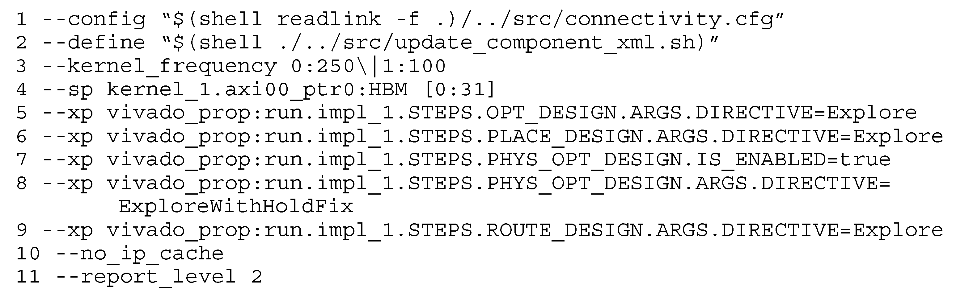
Listing 1. An example of v++ parameters for the improvement of the final clock frequency of XRT-managed kernels in the Vitis design flow. The --kernel_frequency 0:250|1:100 parameter indicates that two clock domains are specified: the first is 250 MHz for the AXI kernel interface and the second is 100 MHz for part of the internal logic inside the kernel. These values are chosen as the reasonable parameters to obtain near the higher possible final frequencies of the AXI kernel bus in new versions of Vitis and the balance of high-throughput requirements of HBM interfaces (which benefit from higher frequencies) with lower power and thermal constraints for processing logic (implemented in parallel with pipelining to ensure the same computations with lower frequencies).
Technologies 13 00266 i001
The v++ parameter also provides the file with connectivity information, where stream connect and SLR mapping can be performed. The requirements for this file also change in different versions of Vitis, and the Xilinx OpenCL Compiler (XOCC) parameters in SDAccel are turned into v++ parameters in Vitis.
To perform any automation in the project before the start of compilation, the possibility of using the --define parameter by specifying the bash file from the project in the Linux shell command was found. The automation running the code from Listing 1 allows one to make a copy of the combined kernel.xo file, extract the XML file from it with text modification, and update the archive before compilation. It saves the compatibility of the kernel with the graphical design flow in Vitis and allows modifications to be performed inside the built kernel.xo files that are compatible only with CLI flow. However, it is also possible to modify the parameters of the configuration files of Vitis itself to make things in graphical design flow impossible by default, such as creating any number of AXI master interfaces in the kernel. From version to version, the kernel creation wizard in Vitis changes allowed several parameters that require consideration during project porting between versions.
The U280 chip includes three distinct SLR areas. SLR0 is connected to two HBM chips through 16 ports, each 256-bit wide. If the interfaces are utilized in the project intensively, the automated placement can result in a reducing of the maximum possible clock frequency for the project that in most cases connected with reducing the system performance. This process can utilize nearly all available resources of certain SLRs, whereas the vendor suggests using just over half. To obtain the detailed log of FPGA resource utilization within Vivado or Vitis design flow, the v++ parameter with verbose output command --report_level 2 should be specified.
The path to report files and the names of files can vary in different versions of integrated envinroments, but the names impl_1_full_util_placed.rpt and impl_1_full_util_routed.rpt are valid for the mentioned versions. Section 14 (SLR CLB Logic and Dedicated Block Utilization) in the obtained report (Figure 3) shows that CLBs in SLR2 are approximately 98.7%, significantly exceeding AMD’s recommendation. To address this issue, two groups of modules associated with HBM were placed in SLR0 to enhance performance (Listing 2).
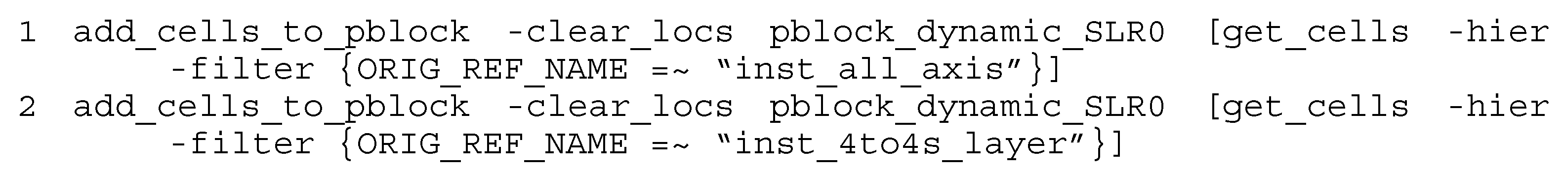
Listing 2. Commands in the TCL file for the Vitis design flow in the new format for the mapping of two groups of modules with names inst_all_axis and inst_4to4s_layer to SLR0.
Technologies 13 00266 i002
The utilization report after applying TCL commands (Figure 4) shows a rebalancing of part of the FPGA resources from SLR1 and SLR2 to SLR0. This action allowed to increase the achievable final clock frequency of the system from 200 MHz to 230 MHz. The opening of Design Checkpoint (DCP) files of a synthesized project in Vivado allows to evaluate the resulting placement of the dynamic region with color highlighting (Figure 5 and Figure 6).
The use of DCP for analysis allows to locate the placement of each module in the project on the FPGA chip. This process requires iterations of attempts of compilation for the specified frequency. After an iteration of compilation, it is possible to check the updated placement and amount of resources for each SLR.

4. Method of Evaluation of FPGA as a Service

4.1. Model of Quality of Service of FPGA as a Service

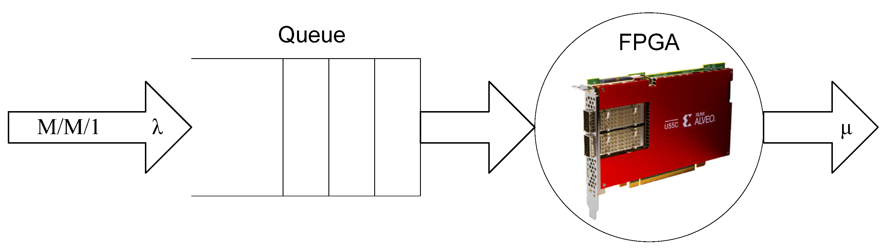
4.1.1. Applying a Queueing Theory for the Modeling of FPGA as a Service

FPGA as a Service allocates resources according to client requirements, utilizing software deployment practices that involve Continuous Integration/Continuous Delivery (CI/CD) pipelines [20]. This methodology facilitates the quick rollout of new features and updates, decreasing the time clients take to bring products to market. FPGA as a Service infrastructure can be built on containerization technology, where each software element is deployed in its container, separated from other applications yet functioning within the same operation systems of a host machine [41]. The cloud service performance metrics include response time, throughput, and network utilization [42,43]. A queuing theory approach utilizing a fork-join queuing system can be employed for QoS cloud environments evaluation [42].
The modeling approach that employs parallel M/M/1 blocks to assess mean response time [43] is mainly the scenario involving two parallel M/M/1 systems. It facilitates in-depth analysis of potential delays and bottlenecks. On the other hand, different techniques for approximating response time can be explored [44], enriching the analysis with alternative perspectives and outcomes.
The response time distribution can be precisely extracted from the resulting model, offering insights into how different parameters influence system performance over time [45]. The overarching system model is depicted as an open M/M/m network if arrival and service times exhibit an exponential distribution. By applying these response time distributions, researchers have discerned the optimal service levels for various scenarios and elucidated the intricate relationship between the maximum number of concurrent tasks that can be handled and the minimum number of virtual machines with the resources required to do so efficiently.
Relying solely on a single queue to represent server performance is insufficient because it overlooks task dependencies. A better strategy considers the system’s response time as a Jackson network. In this model, the server’s performance and the network’s efficiency are vital elements that significantly influence the overall response time of the system [46]. This approach accurately depicts cloud systems by identifying client, server, and network component dynamics.
The analyses provide valuable examples of various modeling architectures and implementations in cloud Platform-as-a-Service (PaaS) systems. This suggests that a similar methodological approach can be applied to the FPGA as a Service domain. Furthermore, to enhance performance and resource utilization, consideration should be given to optimizing how service-oriented cloud applications are situated in relation to virtual machines (VMs) [46]. The findings indicate that queuing theory is a widely adopted framework for constructing models that measure various QoS service metrics (Figure 7).
Given that FPGA as a Service operates under core principles, like those found in traditional cloud services, it is recommended that queuing theory be employed for its modeling and analysis. This approach can accurately simulate the dynamics within an FPGA as a Service system, encompassing the interactions between the clients, servers, and available computing resources. By integrating queuing theory models into their operations, cloud service providers can drive performance, reliability, and scalability improvements, ultimately enhancing the overall service experience for their clients.

4.1.2. Building of FPGA as a Service Model

The request processing within the FPGA as a Service can be observed as a queue consisting of several service blocks, each functioning as separate independent service channels. These channels are consistently prepared to manage incoming requests, facilitating a dynamic task flow. However, the unpredictable nature of requests, combined with variable service times, presents challenges that may lead to significant congestion at the entrance of the queue. In such scenarios, requests may become either excessively queued or may exit the system without adequate oversight.
This can create inefficiencies, as the queue may experience periods of underutilization or complete idleness at different periods of time. Furthermore, if the duration for processing requests increases, there is a risk that a considerable number of sub-requests may accumulate within the synchronization buffer, potentially surpassing acceptable thresholds. This accumulation could result in service failures or a deterioration in service quality. To effectively address and analyze the complexities associated with the operation of the FPGA as a Service system, we propose utilizing a queuing model represented as an open Jackson network.
Let examine an open queue network consisting of K nodes, where each node represents an M/M/n queuing system. The k-th node has nk serving devices. Clients arrive at the k-th node from the external environment according to a Poisson process with an arrival rate of λk. Additionally, requests may also be routed from other nodes to the k-th node, and clients can visit the same node multiple times.
The network features a single inbound server that serves as the entry point. This server functions as a load-balancing device, directing user requests to the processing servers, which are represented as nodes in the system (i = 1, 2, …, m). The load balancer is modeled as an M/M/1 queue, with arrival and service rates that follow an exponential distribution, characterized by parameters λ (arrival rate) and L (service rate), where it is ensured that λ < L. The processing servers are modeled as an M/M/m queuing system, with a service speed denoted as μ, where μ = μi for each processing node (i = 1, 2, …, m).
The output server (OS) represents a component of cloud architecture responsible for transmitting response data to clients that have submitted requests. Conversely, the client server (CS) issues exponentially distributed queries with a parameter λ to the incoming input server (IS) and receives responses from the cloud architecture. The CS continues to receive files or fragments of files until the client’s request is entirely fulfilled. Both the OS and CS can be effectively modeled using the M/M/1 queue framework, which characterizes connections to the servers through exponential arrival and service distributions that operate independently [47]. This model provides a viable representation of the capacity distribution for clients departing from the server.
According to Jackson’s theorem, the overall average arrival rate can be computed by aggregating the response time of the external system with the response times of the internal nodes. By utilizing Jackson’s theorem, we can derive γ, the arrival rate of the exponential distribution at both nodes, expressed mathematically as follows:
γ = λ 1 p   ,
where p is the state distribution of probability for the node for the Poisson process.
The subsequent formula outlines the response time (T) of the cloud architecture as follows:
T = T I S + T P S + T O S + T C S   ,
where TIS, TPS, TOS, and TCS are the components of the total response time for parameters of the input server, process service (PS), output server, and client server, respectively.
TIS represents the response time of the input server, which functions as a load-balancing device/service. The input server is modeled using an M/M/1 queue. Therefore, the formula for determining the queue model for the cloud system is based on the response time for the M/M/1 queue as follows:
T I S = 1 L 1 λ L ,
where λ represents the arrival rate, while L denotes the service speed of the input server.
TPS reflects the response time of process service nodes responsible for managing user requests. These nodes are modeled using an M/M/M queue framework. The associated formula is employed to accurately calculate the response time of the queue as follows:
T P S = 1 μ + C ( m , ρ ) m λ γ ,
where m is the number of processing elements, while γ and μ = μi, i = 1 … m denote the arrival and service rates for each processing element, respectively.
A fundamental element of Jackson’s theorem is the independence of each node in relation to others. The use of the Erlang formula facilitates the calculation of state probabilities, resulting in a significant simplification of the processes involved in determining state-space probabilities. In this case, the process of work can be represented as the simple chain.
The term C ( m , ρ ) represents the Erlang formula, which calculates the probability of a new client joining the M/M/m queue. The Erlang formula is defined as follows:
C m , ρ = m ρ m m ! · 1 1 ρ k = 0 m 1 m ρ k k ! + m ρ m m ! · 1 1 ρ ,
ρ = γ μ .
TOS refers to the response time of the output server, which sends data back to a client. Its operation can be modeled as an M/M/1 queue. The service speed of this server is defined as O/F, where O represents the OS’s average bandwidth speed (measured in bytes per second) and F denotes the average size of the system response files. This formula is used to determine the response time as follows:
T O S = F O 1 γ O F ,
T O S = F O γ F ,
TCS signifies the response time of a client server (CS) system involved in data reception. This operation is effectively modeled using an M/M/1 queue framework. In this scenario, the service speed is expressed as C/F, where C represents the average bandwidth rate of the client server in bytes per second and F indicates the average size of the system’s response files in bytes. The definition of the response time is articulated as follows:
T C S = F C 1 γ C F ,
T C S = F C γ F ,
The service’s performance should be tailored to meet the specific needs of its application area. The uniqueness of this model is the consideration of the form of processing requests at the side of the host computer within the interaction with FPGA. This process of interaction with accelerator cards also adds to the delay of interaction over the XRT framework.

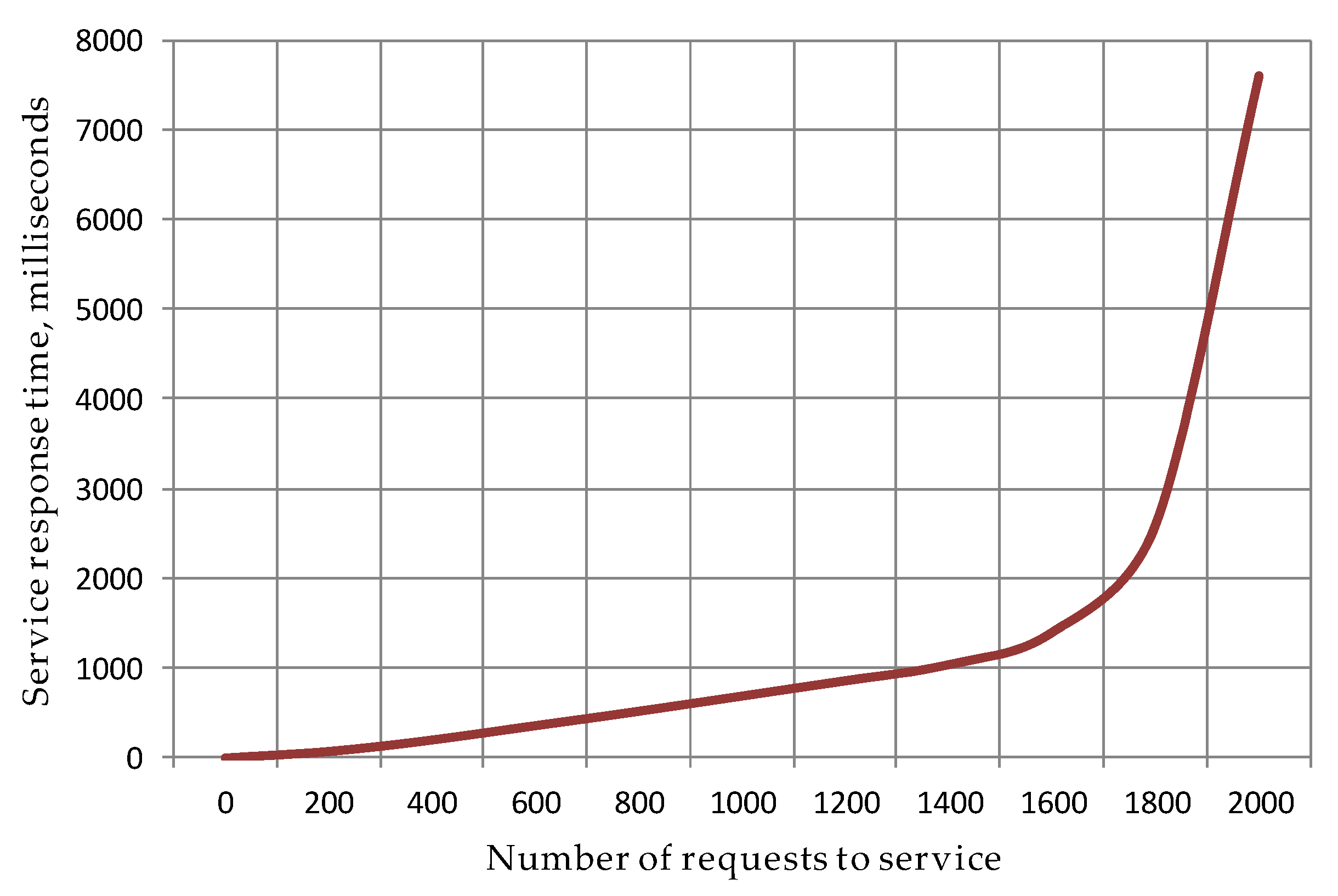
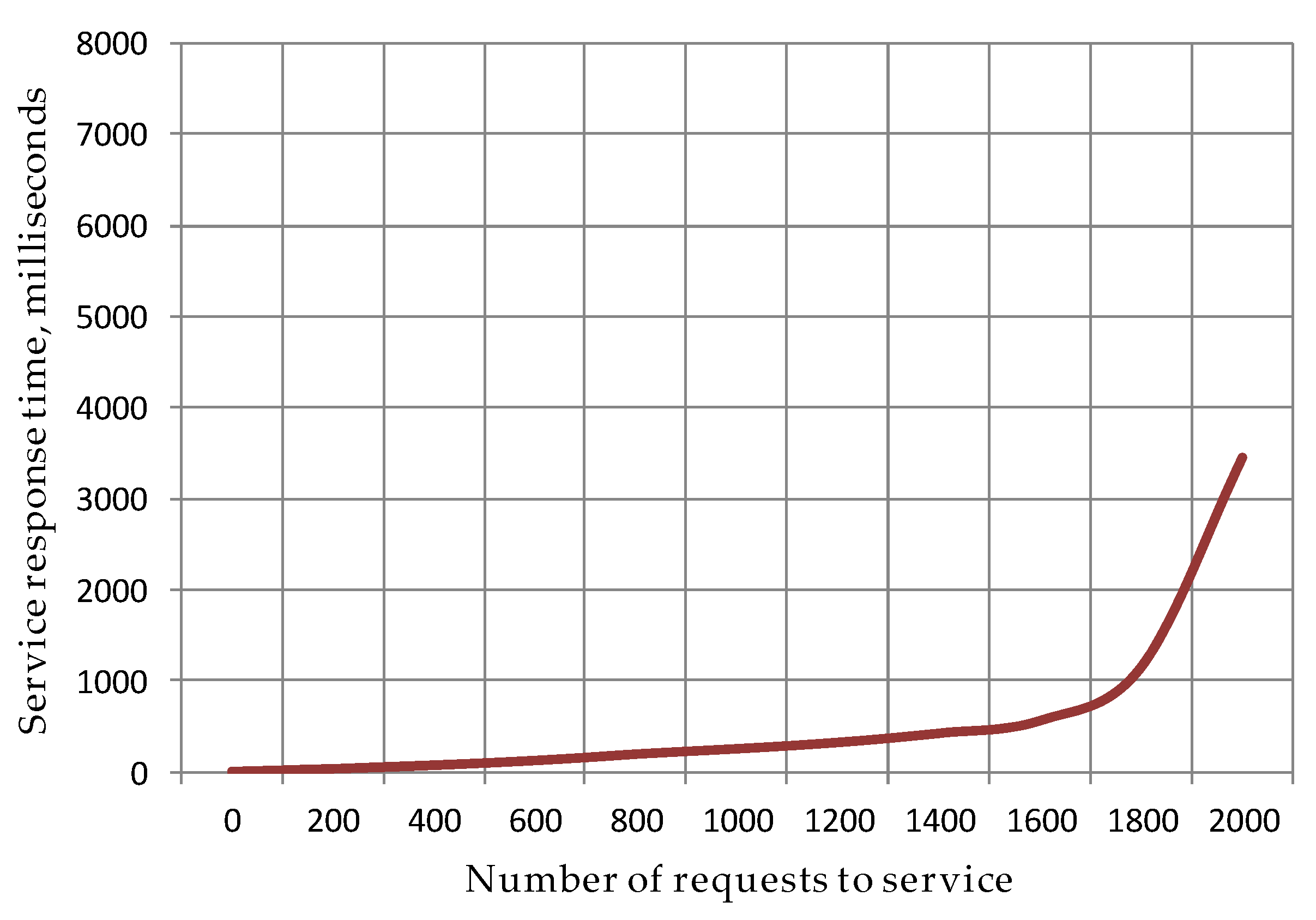
4.1.3. Evaluation of Response Time of FPGA as a Service

Data processing throughput is a key performance indicator for a service’s end users. Additionally, the response time of individual service elements is crucial. Assessing latency response metrics alongside throughput metrics allows for better forecasting of system performance based on request volume.
This evaluation identifies potential bottlenecks early on and provides valuable insights for creating or optimizing services. The proposed FPGA as a Service model enables the evaluation of service components by assigning specific values to their individual parameters. For this test case, the architecture included servers built from both virtual and host machines, which comprised an input server, an output server, and a client server. VMAccel provided virtual machines with the same U50 cards as those installed on the main machine.
According to the simulation results, the most significant improvement was observed when transitioning from one to two virtual machines (see Figure 8 and Figure 9). Adding one server resulted in a quicker response time. This enhancement is particularly valuable in FPGA applications for 5G network infrastructure, where such performance gains would enable telecommunications equipment to process twice the number of network packets before experiencing significant latency issues. For network operators, this translates to more efficient bandwidth allocation during peak usage periods, reducing the need for costly infrastructure expansion while maintaining quality of service standards.
Based on the model, the response time is influenced by various parameters, including the communication latency of the XRT-controlled kernel with the host application. To find a way to reduce delays, it is necessary to investigate the dependence of the coefficient of the interaction delay from a number of installed parallel FPGA accelerator cards.

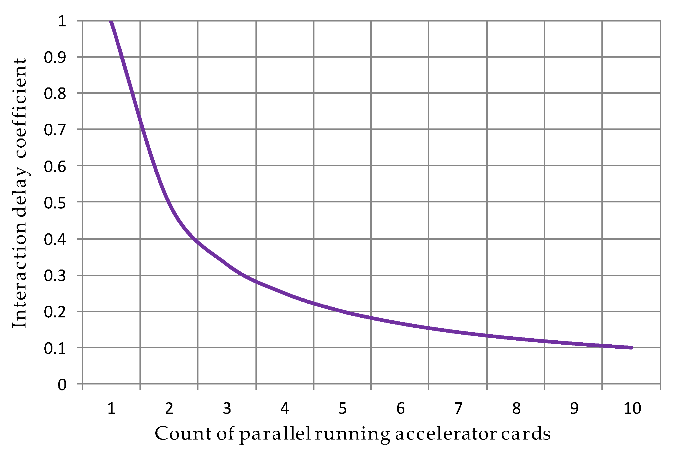
4.2. Model of Delays of FPGA as a Service

The response time latency can be reduced by changing the communication method with the kernel or through the penalty of acceleration by utilizing multiple cards for a single task. If the host application requests tasks using multiple FPGAs in parallel, the latency for the user will be equivalent to that of a single chip. However, in this scenario, the number of processed datasets will be multiplied by the number of cards operating in parallel.
This indicates that the kernel communication delay’s contribution to the total data processing delay depends on the number of concurrently operating FPGA accelerator boards. A coefficient must be applied to obtain an accurate measure of latency per dataset. This k d e l a y coefficient is derived from dividing one by the number of the cards as follows:
k d e l a y = 1 n F P G A ,
where n F P G A is the number of installed FPGA accelerator cards controlled by the same host application.
The simulation results indicated that for two parallel cards, the kernel communication delay for one dataset is half its value when using a single card. Increasing the number of cards enhances FPGA as a Service synchronization and diminishes the impact of kernel communication delay (see Figure 10). This enhancement reduces total response time, which could be critical for real-time applications, such as financial trading platforms, where millisecond advantages translate to significant competitive edges. For enterprise cloud deployments, this optimization could reduce operational costs for a typical mid-sized application stack through more efficient resource utilization. Additionally, in data-intensive research environments, such improvements enable processing larger datasets without proportional increases in computation time, potentially accelerating research timelines by weeks.
This finding underscores the importance of organizing parallel processing of a single task across all available FPGA accelerator cards to mitigate the effects of communication delay. This implies that if there are n cards and n tasks, organizing a single processing stream using n accelerators is advantageous rather than creating n parallel streams. The remaining tasks wait in a queue while the current one is processed in parallel on n cards. This concept is based on and operates effectively for FPGA projects managed by XRT.
These iterative evaluations of delay and throughput results for the service enable adjustments to the parameter values of individual components according to the proposed steps. Optimizing the system with appropriate parameter values can reduce service response time and enhance throughput.

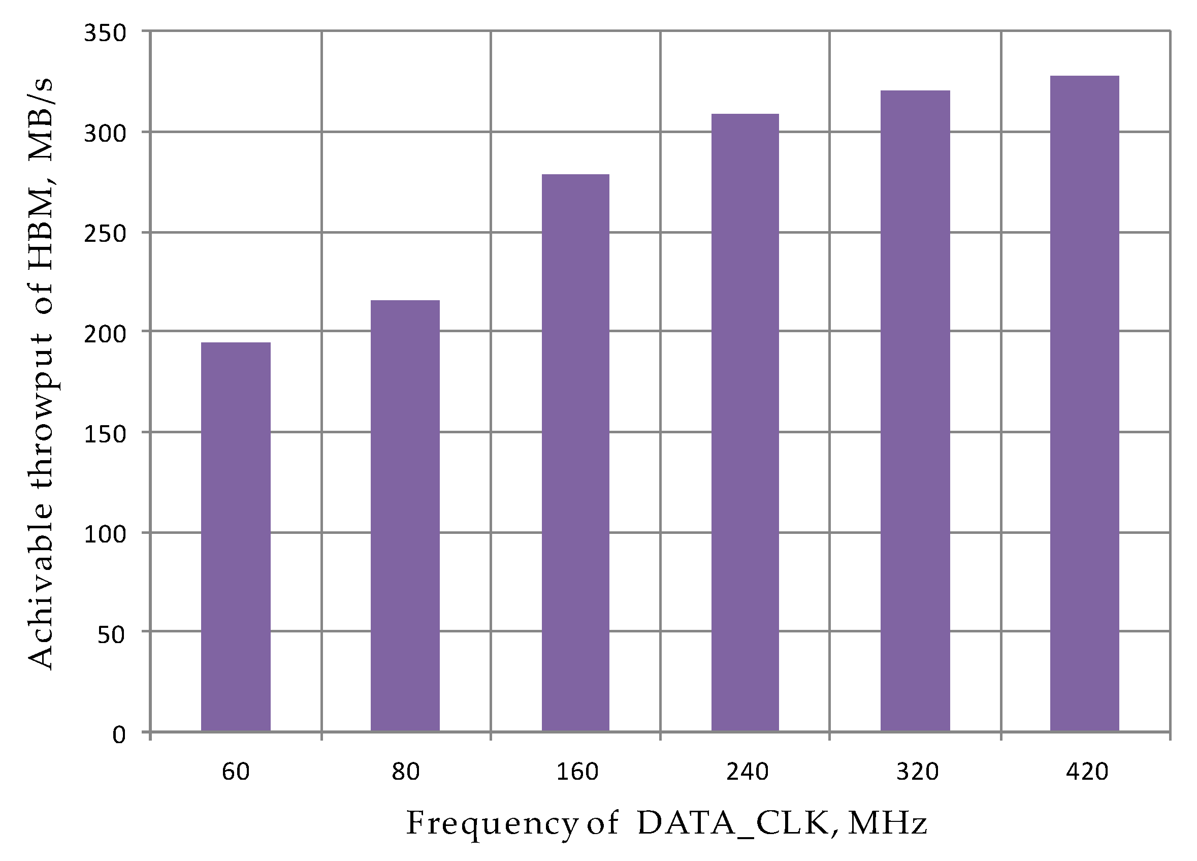
4.3. Evaluation of Memory Throughput of FPGA as a Service

The performance of HBM memory influences the entire performance of memory-intensive projects. The known clock frequency of AXI interfaces with the connection of buses to each memory controller port allows the throughput to be predicted for the linear reading of a block of data. But, at the same time, increasing the frequency also increases the power consumption and the requirements for the project during movement to new versions of the shells, XRT frameworks, and integrated environments.
A significant part of practical tasks requires out-of-order processing of requests to memory in a random manner. It turned out that the throughput of the memory, in this case, does not linearly depend on the frequency of CLK of the AXI bus (Figure 11).
The obtained throughput measurement results consider the work with all available HBM channels. The rising frequency shows the saturation for random readings not described directly in the chips’ documentation. The vendor over the official support mechanism proves that the behaviors of the throughput in random and out-of-order manners of reading can be very nonlinear. It is necessary to consider selecting a reasonable final frequency for the project to maintain the power consumption and heating of the FPGA accelerator at a practically reasonable point. In this project, the 230–240 MHz frequency allows obtaining 94 percent of the maximum achievable throughput in this reading mode. This means that it is unreasonable to increase the frequency any higher if no other logic influences the performance system.

4.4. Steps for Reducing Delays of FPGA as a Service Built on the Xilinx Platform

The service latency based on FPGA includes delays in its various components. Projects implemented using the XRT framework demonstrate latency during kernel execution, which is influenced by the method of communication between the kernel and the host application. This communication process is essential for transferring data and parameters to the kernel and executing the functions that must be accelerated by FPGA.
The percentage of communication phase time relative to the kernel’s overall execution time can vary, depending on the duration of a single kernel iteration. The longer the computation time, the lesser the contribution of communication to the total kernel execution time. Typically, this duration does not exceed a few seconds, a characteristic influenced by the nature of system-level communication implemented with the FPGA accelerator board [23].
However, Xilinx provides various communication modes with XRT-controlled kernels [48]. A pipelined communication mode can mitigate the impact of request delays on overall execution time, though developers must put in additional effort.
Enhancing the FPGA implementation performance is crucial to reducing computation or kernel startup times. This performance is contingent upon the kernel’s clock frequency, which can be set as a parameter (v++) in the Vitis project [36]. However, the final clock frequency after compilation depends on project optimization and may be lower than the specified value. Adhering to timing closure techniques is advisable to improve synchronization parameters in the FPGA project [35].
The proposed response time model for FPGA as a Service can be utilized to evaluate delays in service implementation and optimize requests and processing. Given the assessment results of latency across the FPGA as a Service component, the following steps can be applied to enhance timing. Increase the dataset size (packet) for a single data processing iteration to reduce the number of kernel launches, which is one of the most labor-intensive operations. Use a pipelined execution model rather than a sequential one for the XRT kernel’s second item. Also, follow synchronization closure as the primary recommendation from Xilinx (also detailed in UG949 [35]) to improve the final clock frequency of the project and, consequently, overall performance. Utilize multiple FPGA accelerator cards in parallel for the same host application to distribute data processing and alleviate request delays.

5. Discussion

This study examines FPGA as a Service, a model in which FPGA resources are delivered over the network using hardware and software tools. The proposed methodology for modeling services based on FPGAs facilitates the representation of requests within these systems through a mathematical formulation framework. This capability enables the identification of bottlenecks and the assessment of their impact on the overall throughput of FPGA-based services.
It is demonstrated that the total delay in implementing such kind of systems comprises two factors: the delay within the silicon chip itself, including the communication delay between individual kernels and the host computer, and the aggregation delay in the server rack with the set of accelerator cards, along with additional latency introduced by the network. The suggested steps for minimizing overall delay and improving system throughput offer a reliable decrease in latency for both the silicon chip and the host machine. These steps also encompass increasing the system’s clock frequency by optimizing the design within the accelerator itself. This is particularly important for implementing resource-intensive AI applications based on various types of neural networks [22].
Due to rapid technological advancements and intense market pressure, the lifecycles of specific projects can be shorter than a few years. Therefore, it is essential to factor in the evolving development environments during the initial planning stages of FPGA projects to minimize risks associated with shifting software and hardware contexts. Utilizing runtime reprogramming techniques significantly streamlines the establishment of FPGA as a Service and the development and validation of artificial intelligence systems and components.
Scaling and parallelization on the architecture level, as well as pipelining and parameterization at the RTL level, allow for the effective deployment of FPGA systems based on resources from commercial cloud infrastructures and data centers. Using the proposed sequence to create scalable pipelined systems reduces the required efforts and the duration of the development process of similar projects for high-performance FPGAs.
An experimental study of the paradigm of continuous runtime reprogramming of software was carried out, which made it possible to formulate the elements of a new sequence of creating projects as a service for cloud infrastructures and data centers. Following the proposed sequence of SLR placement for the movement of the part of the project components from one SLR to another allowed for the increase of the system clock frequency of the prototyped system from 200 MHz to 230 MHz. The proposed method’s practical application reduces project modification efforts when switching to a new version of the development environment or continuously specifying the requirements for such a system.

6. Conclusions

The concept of developing cloud services utilizing FPGA-based services to enhance computational performance has been described and discussed. The analysis demonstrated that implementing FPGA acceleration for compute-intensive workloads performed better than CPU and GPU implementations while retaining less power consumption.
An analytical review of the history of product development by leading manufacturers of programmable logic devices has been observed, including an analysis of the dynamics of changes in development environments. A comparative assessment of development and testing boards has also been carried out. Practical experience in transitioning to new solutions for developing programmable logic systems driven by the rapid growth of technology has been examined. The process of porting projects to new development environments for programmable logic devices has been addressed, showing that the pace of technological advancement drives the need for this transition. It has been demonstrated that dynamic in-system programming significantly simplifies the development process of FPGAs as a Service.
The stages of building projects for artificial intelligence systems utilizing programmable logic devices have been explored, covering the development tools, analyzing the essential elements, and reviewing the available components for their support. It has been established that the dynamics of changing development environments should be considered when planning FPGA projects to mitigate risks. The analysis revealed that the programming process for FPGA-based projects using accelerator boards introduces delays caused by various factors, including data transfer latency between the kernel and the host computer, limited project clock frequency, and a fixed number of cards operating in parallel.
A modeling-based evaluation approach is proposed to improve the deployment time of FPGA as a Service. Using queuing theory, analytical models were developed to describe the operation of FPGA as a Service. Key parameters for a service organization, including the number of requests, server processing speed, and internal service performance, were analyzed. Based on the proposed model, the response time of FPGA as a Service was assessed to identify opportunities for performance enhancement. The differences in response time and internal delays for varying numbers of installed FPGA accelerator boards were demonstrated.
To improve service delivery times for FPGA-based systems, a set of optimization steps was proposed that can be applied to systems in the development stage and to existing projects that allow for modification and optimization. The suggested steps include increasing the size of data blocks processed in the FPGA by each kernel, changing the communication model with the kernel from sequential to pipelined, adhering to timing closure techniques, and utilizing more FPGA accelerator cards in parallel to distribute request latency.
A key contribution to this research is the model for designing the cloud computing architecture for FPGA as a Service. It considers the possibility of using elements of queuing theory to analyze the performance and reliability of FPGA as a Service and FPGA technology. Queuing theory and Jackson networks were selected to evaluate performance from a response time perspective, formulating recommendations for improving technical characteristics.
The methodology proposed in this paper for calculating cloud service performance parameters can simplify identifying bottlenecks in service implementation. This enhances the reliability of such systems and improves overall system performance by reducing delays at various stages of request processing. Another aspect of this outcome is the reliability factor, which is based on the modified operation of the service when utilizing the proposed optimization steps. This improves request processing for FPGA as a Service.
The study’s contribution signifies a step forward in modeling FPGA-based services suitable for AI applications. Advancement of this methodological and technological foundation will guide future research and development. Further research may strengthen the methodological base for describing the constituent parameters of such systems with CI/CD, providing an analytical opportunity to perform a numerical evaluation of characteristics based on priority parameters.

Author Contributions

Conceptualization, A.P. and V.K.; methodology, A.P. and V.K.; software, A.P.; validation, V.K.; formal analysis, A.P. and V.K.; investigation, A.P. and V.K.; resources, A.P. and V.K.; data curation, A.P. and V.K.; writing—original draft preparation, A.P. and V.K.; writing—review and editing, V.K.; visualization, A.P. and V.K.; supervision, A.P.; project administration, A.P. All authors have read and agreed to the published version of the manuscript.

Funding

This research received no external funding.

Institutional Review Board Statement

Not applicable.

Informed Consent Statement

Not applicable.

Data Availability Statement

The original contributions presented in the study are included in the article; further inquiries can be directed to the corresponding author.

Acknowledgments

The authors are grateful to all teachers who helped obtain knowledge and aspiration for the study of and interest in fundamental science.

Conflicts of Interest

The authors declare no conflicts of interest.

References

  1. Yu, K.; Kim, M.; Choi, J.R. Memory-Tree Based Design of Optical Character Recognition in FPGA. Electronics 2023, 12, 754. [Google Scholar] [CrossRef]
  2. Perepelitsyn, A. Methodology of deployment of dependable FPGA based Artificial Intelligence as a Service. Radioelectron. Comput. Syst. 2024, 3, 156–165. [Google Scholar] [CrossRef]
  3. Mao, N.; Yang, H.; Huang, Z. An Instruction-Driven Batch-Based High-Performance Resource-Efficient LSTM Accelerator on FPGA. Electronics 2023, 12, 1731. [Google Scholar] [CrossRef]
  4. Faizan, M.; Intzes, I.; Cretu, I.; Meng, H. Implementation of Deep Learning Models on an SoC-FPGA Device for Real-Time Music Genre Classification. Technologies 2023, 11, 91. [Google Scholar] [CrossRef]
  5. Lattice Unveils First FPGAs on FD-SOI. Available online: https://www.eetimes.com/lattice-unveils-first-fpgas-on-fd-soi/ (accessed on 30 October 2024).
  6. Barkalov, A.; Titarenko, L.; Krzywicki, K.; Saburova, S. Improving Characteristics of FPGA-Based FSMs Representing Sequential Blocks of Cyber-Physical Systems. Appl. Sci. 2023, 13, 10200. [Google Scholar] [CrossRef]
  7. FinFET FPGA Market Size, Growth and Forecast from 2023–2030. Available online: https://www.linkedin.com/pulse/finfet-fpga-market-size-growth-forecast-from-2023-2030-1i3ve (accessed on 30 October 2024).
  8. Tetskyi, A. Penetration testing of FPGA as a Service components for ensuring cybersecurity. Aerosp. Tech. Technol. 2023, 6, 95–101. [Google Scholar] [CrossRef]
  9. Song, X.; Lu, R.; Guo, Z. High-Performance Reconfigurable Pipeline Implementation for FPGA-Based SmartNIC. Micromachines 2024, 15, 449. [Google Scholar] [CrossRef]
  10. Goz, D.; Ieronymakis, G.; Papaefstathiou, V.; Dimou, N.; Bertocco, S.; Simula, F.; Ragagnin, A.; Tornatore, L.; Coretti, I.; Taffoni, G. Performance and Energy Footprint Assessment of FPGAs and GPUs on HPC Systems Using Astrophysics Application. Computation 2020, 8, 34. [Google Scholar] [CrossRef]
  11. Kolasiński, P.; Poźniak, K.T.; Wojeński, A.; Linczuk, P.; Kasprowicz, G.; Chernyshova, M.; Mazon, D.; Czarski, T.; Colnel, J.; Malinowski, K.; et al. High-Performance FPGA Streaming Data Concentrator for GEM Electronic Measurement System for WEST Tokamak. Electronics 2023, 12, 3649. [Google Scholar] [CrossRef]
  12. Kulanov, V.; Perepelitsyn, A. Method of creation and deployment of FPGA projects resistant to change of requirements and development environments for cloud infrastructures. Aerosp. Tech. Technol. 2023, 5, 87–97. [Google Scholar] [CrossRef]
  13. Vivado Design Suite Reference Guide, Model-Based DSP Design Using System Generator, UG958 (v2020.2). 18 November 2020. Available online: https://docs.amd.com/r/en-US/ug958-vivado-sysgen-ref (accessed on 29 October 2024).
  14. UltraScale Architecture Memory Resources User Guide, UG573 (v1.13). 24 September 2021. Available online: https://docs.amd.com/v/u/en-US/ug573-ultrascale-memory-resources (accessed on 29 October 2024).
  15. Vivado Design Suite Properties Reference Guide, UG912 (v2022.1). 8 June 2022. Available online: https://www.xilinx.com/support/documents/sw_manuals/xilinx2022_1/ug912-vivado-properties.pdf (accessed on 29 October 2024).
  16. Vitis High-Level Synthesis User Guide, UG1399 (v2024.1). 3 July 2024. Available online: https://docs.amd.com/r/en-US/ug1399-vitis-hls (accessed on 29 October 2024).
  17. Choi, S.; Yoo, H. Approaches to Extend FPGA Reverse-Engineering Technology from ISE to Vivado. Electronics 2024, 13, 1100. [Google Scholar] [CrossRef]
  18. Taj, I.; Farooq, U. Towards Machine Learning-Based FPGA Backend Flow: Challenges and Opportunities. Electronics 2023, 12, 935. [Google Scholar] [CrossRef]
  19. Alveo U280es1: How to Update SC Version on System Shell? Adaptive SoC & FPGA Support. Available online: https://adaptivesupport.amd.com/s/question/0D52E00006hpFyRSAU/alveo-u280es1-how-to-update-sc-version-on-system-shell (accessed on 29 October 2024).
  20. Perepelitsyn, A.; Kulanov, V.; Zarizenko, I. Method of QoS evaluation of FPGA as a Service. Radioelectron. Comput. Syst. 2022, 4, 153–160. [Google Scholar] [CrossRef]
  21. Alveo U50 Data Center Accelerator Card Data Sheet, DS965 (v1.8). 23 June 2023. Available online: https://docs.amd.com/r/en-US/ds965-u50 (accessed on 29 October 2024).
  22. Perepelitsyn, A.; Fesenko, H.; Kasapien, Y.; Kharchenko, V. Technological Stack for Implementation of AI as a Service based on Hardware Accelerators. In Proceedings of the 2022 IEEE 12th International Conference on Dependable Systems, Services and Technologies DESSERT, Athens, Greece, 9–11 December 2022; 5p. [Google Scholar] [CrossRef]
  23. Perepelitsyn, A.; Kulanov, V. Technologies of FPGA-based projects Development Under Ever-changing Conditions, Platform Constraints, and Time-to-Market Pressure. In Proceedings of the 2022 12th International Conference on Dependable Systems, Services and Technologies DESSERT, Athens, Greece, 9–11 December 2022; 5p. [Google Scholar] [CrossRef]
  24. AMD. Versal AI Core Series Product Selection Guide, XMP452 (v1.15). Available online: https://docs.amd.com/v/u/en-US/versal-ai-core-product-selection-guide. (accessed on 24 April 2025).
  25. Di Mauro, M.; Liotta, A.; Longo, M.; Postiglione, F. Statistical Characterization of Containerized IP Multimedia Subsystem through Queueing Networks. In Proceedings of the 2020 6th IEEE Conference on Network Softwarization, NetSoft, Ghent, Belgium, 29 June–3 July 2020; pp. 100–105. [Google Scholar] [CrossRef]
  26. Pilz, S.; Porrmann, F.; Kaiser, M.; Hagemeyer, J.; Hogan, J.M.; Rückert, U. Accelerating Binary String Comparisons with a Scalable, Streaming-Based System Architecture Based on FPGAs. Algorithms 2020, 13, 47. [Google Scholar] [CrossRef]
  27. Regoršek, Ž.; Gorkič, A.; Trost, A. Parallel Lossless Compression of Raw Bayer Images on FPGA-Based High-Speed Camera. Sensors 2024, 24, 6632. [Google Scholar] [CrossRef]
  28. Alveo U280 Data Center Accelerator Card, UG1314 (v1.1). 15 June 2023. Available online: https://docs.amd.com/r/en-US/ug1314-alveo-u280-reconfig-accel (accessed on 29 October 2024).
  29. AMD. AMD Alveo™ U55C Data Center Accelerator Card. Available online: https://www.amd.com/en/products/accelerators/alveo/u55c.html (accessed on 29 October 2024).
  30. AMD. VHK158 Evaluation Board User Guide, UG1611 (v1.0). Available online: https://docs.xilinx.com/r/en-US/ug1611-vhk158-eval-bd (accessed on 28 October 2024).
  31. AMD. Alveo UL3524 Ultra Low Latency Trading Data Sheet, DS1009 (v1.1). Available online: https://docs.xilinx.com/r/en-US/ds1009-ul3524 (accessed on 29 October 2024).
  32. AMD. Alveo Portfolio Product Selection Guide, XMP451 (v2.1). Available online: https://docs.amd.com/v/u/en-US/alveo-product-selection-guide (accessed on 29 October 2024).
  33. Xilinx. SDAccel Environment User Guide, UG1023 (v2019.1). Available online: https://www.xilinx.com/support/documents/sw_manuals/xilinx2019_1/ug1023-sdaccel-user-guide.pdf (accessed on 29 October 2024).
  34. Xilinx. XRT Controlled Kernel Execution Models. Available online: https://xilinx.github.io/XRT/master/html/xrt_kernel_executions.html (accessed on 29 October 2024).
  35. Xilinx. UltraFast Design Methodology Guide for the Vivado Design Siute, UG949 (v2019.2). Available online: https://docs.xilinx.com/v/u/2019.2-English/ug949-vivado-design-methodology. (accessed on 29 October 2024).
  36. Xilinx. Vitis Unified Software Platform Documentation: Application Acceleration Development, UG1393 (v2019.2). Available online: https://docs.xilinx.com/r/en-US/ug1393-vitis-application-acceleration. (accessed on 28 February 2020).
  37. Xilin. Xilinx_Base_Runtime Release Notes. Available online: https://github.com/Xilinx/Xilinx_Base_Runtime (accessed on 29 October 2024).
  38. Xilinx. List of Corresponding Versions of XRT and Supported Board Shell Versions for Alveo FPGA Cards. Available online: https://github.com/Xilinx/Xilinx_Base_Runtime/blob/master/conf/spec.txt (accessed on 29 October 2024).
  39. Goswami, P.; Bhatia, D. Congestion Prediction in FPGA Using Regression Based Learning Methods. Electronics 2021, 10, 1995. [Google Scholar] [CrossRef]
  40. Gabrielli, A.; Alfonsi, F.; Annovi, A.; Camplani, A.; Cerri, A. Hardware Implementation Study of Particle Tracking Algorithm on FPGAs. Electronics 2021, 10, 2546. [Google Scholar] [CrossRef]
  41. Containerizing Alveo Accelerated Applications with Docker. Available online: https://xilinx.com/developer/articles/containerizing-alveo-accelerated-application-with-docker.html (accessed on 27 January 2020).
  42. Tsimashenka, I.; Knottenbelt, W.J. Reduction of Subtask Dispersion in Fork-Join Systems. In Computer Performance Engineering. EPEW 2013; Lecture Notes in Computer Science; Springer: Berlin/Heidelberg, Germany, 2013; Volume 8168, pp. 325–336. [Google Scholar] [CrossRef]
  43. Gorbunova, A.V.; Zaryadov, I.S.; Samouylov, K.E. A Survey on Queuing Systems with Parallel Serving of Customers. Part II. Discret. Contin. Models Appl. Comput. Sci. 2018, 26, 13–27. [Google Scholar] [CrossRef]
  44. Gaidamaka, Y.; Sopin, E.; Talanova, M. A Simplified model for performance analysis of cloud computing systems with dynamic scaling. In Distributed Computer and Communication Networks: Control, Computation, Communications; Springer: Berlin/Heidelberg, Germany, 2015; pp. 75–86. [Google Scholar]
  45. Kothandaraman, D.; Kandaiyan, I. Analysis of a Heterogeneous Queuing Model with Intermittently Obtainable Servers under a Hybrid Vacation Schedule. Symmetry 2023, 15, 1304. [Google Scholar] [CrossRef]
  46. Gad-Elrab, A.A.A.; Alzohairy, T.A.; Raslan, K.R.; Emara, F.A. Genetic-Based Task Scheduling Algorithm with Dynamic Virtual Machine Generation in Cloud Computing. Int. J. Comput. 2021, 20, 165–174. [Google Scholar] [CrossRef]
  47. Sai Sowjanya, T.; Praveen, D.; Satish, K.; Rahiman, A. The queueing theory in cloud computing to reduce the waiting time. Int. J. Comput. Sci. Eng. Technol. 2011, 1, 110–112. [Google Scholar]
  48. AMD. What is XRT/AMD Runtime Library? Vitis Tutorials: Getting Started, XD098 (v2025.1). Available online: https://docs.amd.com/r/en-US/Vitis-Tutorials-Getting-Started/What-is-XRT/AMD-Runtime-Library (accessed on 26 March 2025).
Figure 1. Evolution over a decade of integrated environments of Xilinx and then AMD.
Technologies 13 00266 g001
Figure 2. Assigned vs. achieved clock frequency: experimental evaluation of kernel_frequency settings and their resulting impact on final clock frequency after compilation in SDAccel for U280es1 with shell version 201830.1. Despite targeting 420–465 MHz, the achieved frequencies vary significantly, underscoring the importance of tuning kernel parameters to approach frequency goals under practical constraints.
Technologies 13 00266 g002
Figure 3. Detailed log with the use of the verbose output command (--report_level 2) after compilation of the project in Vitis shows unbalanced FPGA resource usage (maximum utilization in SLR1 and SLR2).
Technologies 13 00266 g003
Figure 4. Detailed log with the use of the verbose output command (--report_level 2) after compilation of the project in Vitis indicates FPGA resource rebalancing when two modules mapped to SLR0 is performed.
Technologies 13 00266 g004
Figure 5. The implemented design of the project with XRT-managed kernels for U280 faced reduced performance because of the limited number of available interconnects between SLRs.
Technologies 13 00266 g005
Figure 6. The representation of the project after the manual placement of two groups of modules (a) from SLR1 and SLR2 to SLR0 for direct connection to HBM to allow improving final frequency (b).
Technologies 13 00266 g006
Figure 7. The representation of the queueing model of FPGA as a Service.
Technologies 13 00266 g007
Figure 8. The response time (T) evaluation for one server.
Technologies 13 00266 g008
Figure 9. The response time (T) evaluation with the use of two servers. Using two servers reduces the service response time by approximately 40% at high request loads (for reference, 2100 requests) compared to a single server.
Technologies 13 00266 g009
Figure 10. The dependence of the data transferring time as part of the entire data processing duration in FPGA depends on the number of installed FPGA accelerated cards.
Technologies 13 00266 g010
Figure 11. The dependence of the throughput of a random reading of HBM in gigabytes per second for the FPGA accelerator card U280es1 with the shell version 201830.1 with XRT-managed kernels on the frequency of clk involved in AXI communication with both memory banks.
Technologies 13 00266 g011
Disclaimer/Publisher’s Note: The statements, opinions and data contained in all publications are solely those of the individual author(s) and contributor(s) and not of MDPI and/or the editor(s). MDPI and/or the editor(s) disclaim responsibility for any injury to people or property resulting from any ideas, methods, instructions or products referred to in the content.

