Abstract
The growing demand for real-time video streaming in power-constrained embedded systems, such as drone navigation and remote surveillance, requires encoding solutions that prioritize low latency. In these applications, even small delays in video transmission can impair the operator’s ability to react in time, leading to instability in closed-loop control systems. To mitigate this, encoding must be lightweight and designed so that streaming can start as soon as possible, ideally even while frames are still being processed, thereby ensuring continuous and responsive operation. This paper presents the design of a hardware implementation of the Logarithmic Hop Encoding (LHE) algorithm on a Field-Programmable Gate Array (FPGA). The proposed architecture is deeply pipelined and parallelized to achieve sub-frame latency. It employs adaptive compression by dividing frames into regions of interest and uses a quantized differential system to minimize data transmission. Our design achieves an encoding latency of between 1.87 ms and 2.1 ms with a power consumption of only 2.7 W when implemented on an FPGA clocked at 150 MHz. Compared to a parallel GPU implementation of the same algorithm, this represents a 6.6-fold reduction in latency at approximately half the power consumption. These results show that FPGA-based LHE is a highly effective solution for low-latency, real-time video applications and establish a robust foundation for its deployment in embedded systems.
1. Introduction
The proliferation of intelligent embedded systems has spread innovation across numerous fields, including industrial automation, remote inspection, and autonomous navigation [1,2]. Many of these systems critically rely on real-time video streams to provide situational awareness [3], enable remote operation [4], or serve as input for control algorithms [5]. For instance, Unmanned Aerial Vehicles (UAVs) use video for applications ranging from emergency patient care [4,6] to infrastructure monitoring, while marine robotics employ camera feeds for underwater exploration [7,8]. In all such applications, the ability to capture, process, and transmit video with minimal delay and power consumption is a must [9].
These real-time systems require two intertwined factors to be optimized: latency and power consumption [10,11]. Latency, defined as the end-to-end delay from image capture to its reconstruction on a remote display, is a critical performance metric. Excessive latency can degrade operator performance and lead to instability in closed-loop control systems, rendering the application unusable [10]. Latency is largely determined by the processing time of the video encoder. Since each additional computational step directly adds to the end-to-end delay, encoder designers are compelled to develop algorithms with low computational complexity to ensure that video can be processed and transmitted within the strict time constraints required by real-time applications. Concurrently, frame losses must be minimized because they deprive the system or operator of vital environmental information. Power consumption presents another hard constraint because these platforms are often battery-powered and operate within strict thermal envelopes. Therefore, the on-board processing, particularly video encoding, must be highly energy efficient [12]. This limitation is usually set by the platform and benefits from the same design practices as latency, namely, low-complexity encoding methods, which focus more on distributing the processing [13].
Video encoding is necessary to manage the large amounts of data generated by high-resolution cameras, which can produce many megabytes per frame at rates of 30, 60, or more frames per second. Conventional codecs such as H.264/AVC and H.265/HEVC achieve high compression ratios but at the cost of significant computational complexity, often requiring power-hungry processors or dedicated application-specific integrated circuits (ASICs), which lack flexibility [14]. To achieve low latency, encoding must be performed in real time, often in parallel with image capture. Protocols like WebRTC are frequently deployed to minimize network-related delays. For example, studies on drone streaming have achieved end-to-end latencies under 200 ms [15,16]. However, the encoding step itself remains a primary bottleneck. As noted in [17], achieving ultra-low latencies (e.g., less than 10 ms) is necessary for enabling truly interactive and safe remote operation. This requires a shift toward lightweight algorithms that facilitate computational parallelism by processing image regions independently [13].
Logarithmic Hop Encoding (LHE) [18,19] was designed to address these trade-offs. It is a computationally simple and robust codec for real-time video that features two key properties ideal for embedded applications. First, it uses elastic downsampling to compress different areas of an image based on their local information content. Second, LHE encodes frames independently without relying on inter-frame data. This eliminates the need for large frame buffers and makes the stream resilient to packet loss. The intra-frame approach ensures that corrupted data in one frame does not affect subsequent ones, and even partially received frames can be decoded, therefore increasing reliability.
Although the algorithmic properties of LHE are well suited for low-latency applications, its performance and efficiency when implemented in hardware have not been extensively explored. Field-Programmable Gate Arrays (FPGAs) present a compelling solution for battery-operated embedded systems that demand both significant computational power and low energy consumption [20,21,22]. Their inherently parallel architecture enables massive data throughput by executing numerous operations simultaneously, supporting real-time tasks like signal processing and video encoding. Unlike general-purpose processors, which incur overhead from instruction fetching and operating systems, FPGAs are configured with custom hardware circuits precisely tailored to the target algorithm. This specialization eliminates unnecessary logic and minimizes power draw, leading to a superior performance-per-watt ratio. Consequently, FPGAs provide the computational horsepower of specialized hardware while retaining the flexibility to be reconfigured. This makes them an ideal platform for power-constrained devices, such as autonomous drones [23,24], wearable sensors [25], and robotics [26], where maximizing operational lifetime without sacrificing performance is necessary.
This article introduces the first FPGA-based implementation of LHE with elastic downsampling, achieving sub-frame latency through a deeply pipelined and parallelized hardware architecture. Our primary objectives are to achieve sub-frame encoding latency and to minimize power consumption. The FPGA-based implementation was compared with a concurrent software implementation using an embedded GPU. The goal of this work is to analyze the suitability of an LHE-FPGA system for real-time video applications on resource-constrained embedded platforms.
The next section presents the LHE algorithm. This is followed by a description of the hardware platform utilized for its implementation and a design of the LHE algorithm tailored for an FPGA architecture. Subsequently, various simulations of the algorithm performed on FPGAs optimized for processing images of different resolutions ( and ) are presented. The latency, power consumption, and scalability of the design are studied and compared against an implementation of the LHE algorithm on a GPU designed for embedded systems (NVIDIA Maxwell GPU with 128 CUDA cores). Furthermore, a laboratory validation of the algorithm using real hardware is presented. Finally, the results are discussed and conclusions are drawn.
2. Materials and Methods
2.1. Logarithmic Hop Encoding
Logarithmic Hop Encoding, or LHE for short, is a video encoding and decoding algorithm designed to minimize encoding times, thus reducing latency in remote control applications, where response time is a priority over bandwidth. It works in the spatial domain by dividing a frame into blocks and encoding the differences between pixels within the same block, minimizing the need to store information. Its mathematical basis has been described in [18]. Here, a summary of its theory of operation and updates made for this particular scenario will be provided.
LHE exploits the Weber–Fechner laws, which state that changes in the human perception of light intensity are proportional to the previous values of the intensity and that the intensity increase for such a change is logarithmic [27]. This means that small differences in pixel intensity before and after encoding will not be perceptible to the human eye. LHE takes advantage of this by calculating the predicted intensity of a pixel based on its surrounding pixels and encoding the error—the difference between the prediction and the real intensity—as one of a set of “hops”. Each “hop” is a discrete step in intensity on a logarithmic scale. As the image is being encoded, the actual value of each step is updated dynamically, based on the values of the previous errors. This process is completely deterministic, meaning that, given one starting value, it can be replicated in the decoder to obtain the same sequence of value updates.
Another feature of LHE that optimizes compression is the fact that different areas of the image may have different levels of detail. For instance, one region may be a background, with little variation in colors and intensities, while another region may have text or complex objects that need a higher level of detail to distinguish. Areas with low detail can be compressed more without losing perceived quality, while other areas may benefit from little to no image compression. To analyze these areas, since the Weber–Fechner laws refer to light intensity, the colors of the image are represented as luminance (Y), which gives an idea of the brightness, and chrominance (U and V), which gives an idea of the hue. The original frame is divided into blocks of the same width and height—typically or , which are exact divisors of some of the most commonly used video resolutions.
For each block, a metric called the perceptual relevance (PR) is computed for the horizontal () and vertical () axes. The PR corresponds to the average of the absolute value of the differences in intensity between adjacent pixels for each axis, given in the interval [0, 1] (with 1 representing the greatest rate of change). The first step for obtaining the PR is calculating the differences between neighboring pixels in the desired axis () and assigning them a “quantum” between 0 and 4 (), according to the thresholds in Table 1. The PR is then calculated using the following formula, where M is the number of differences for which :

Table 1.
Thresholds for the luminance difference quanta used in the calculation of PR.
Finally, the is adjusted so that its range fits within the [0, 1] interval:
and is then discretized into one value of the set .
Once the PR is computed, each block is compressed using downsampling. An independent downsampling factor is used in both axes by defining a plane predicted pixel value or PPP, which corresponds to the number of pixels that are averaged together for the downsampled block, according to the following equation:
Here, the CF or “compression factor” is a factor that is set before streaming and controls the sensitivity of the mapping from PR to PPP (aggressiveness when downsampling). The higher the CF, the more the image will be downsampled even with high PRs. is generally 8.
For downsampling, the PPP is quantized to an integer number, so pixels are averaged together in groups of 1, 2, 4, or 8. The higher the PR, the less the block will be compressed. Each LHE block is first downsampled horizontally and then vertically. Note that different downsampling factors can be used for each axis because the PR can be different for each of them. This is meant to preserve information about edges, while still compressing similar colors or backgrounds.
Lastly, the hops are calculated for each compressed block. The process begins in the upper-left corner of the block. For the remaining pixels, a predicted value is calculated as the average of two neighboring pixels, typically the one to its left and the one in the upper-right corner. For pixels close to the borders of the image, a compromise is made by taking other neighbors. Figure 1 shows the possible combinations of neighbors used to form a prediction. The chosen hop value is the one closer to the difference between the pixel’s actual and predicted values. Then, the reference point for the hops is recalculated by readjusting the difference between the central hop (which means no error) and the first hop (the smallest possible error). The rest of the hops all change relative to this difference—the difference in value between two hops is a power of for positive hops and a power of for negative hops. The most important variables of the algorithm for calculating the hops are the value for the smallest hop , which establishes the sensitivity of the predictions, and a gradient, which is a small increment in the prediction based on the tendency of the image, to correct possible deviations. Both of them are updated after each prediction. When the difference between neighbors is large, the colors of intensities are very variable within the block, so the values of the parameters are increased. LHE predicts well when the neighboring pixels are similar, so the average of the two makes for a good prediction. However, in cases where the value for these pixels is very different, the prediction is not accurate. In these cases, when the difference between neighboring pixels is above a threshold, the value of is set to its highest value, instead of waiting for slower changes in gradient. This is called “immediate ”. Code that provides a more detailed description of the algorithm can be found in the GitHub repository linked in the Data Availability Statement.
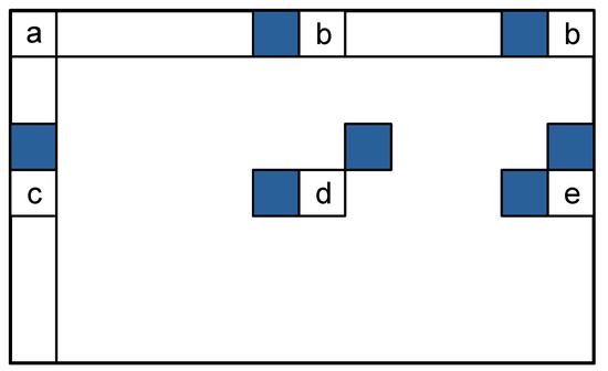
Figure 1.
Possible pixel positions inside LHE blocks: (a) first pixel, (b) pixel from the first line, (c) pixel from the first column, (d) pixel from the middle of the block and (e) pixel from the last column, with the neighboring pixels used to calculate their predicted value highlighted in color.
The LHE algorithm lends itself to parallelization and quantization at several points. First of all, since the image is divided into blocks, each block, or set of partial results for each block, can be treated separately from the rest, and several blocks can be processed simultaneously. The different processing stages can be pipelined easily: while a series of blocks is undergoing downsampling, the next batch of blocks can already have their perceptual relevance computed, and so on. The decisions on quantization and encoding can affect the downsampling and hop calculation processes. When calculating the PR, rather than averaging the value of the differences directly, each difference is classified into one of five quanta with four thresholds. Then the PR is also discretized into one of . This results in a possible number of points to average in the set . Since the intensity values for the hops can be updated in the receiver following the same algorithm as the transmitter, only the number of the hop (how far the jump in intensity should be) needs to be transmitted. For the LHE implementation being discussed, this means an integer value in the range .
This system of parallelization and discrete values can be translated well into platforms for accelerated computing, such as GPUs and FPGAs, since operations within a small set of well known conditions are more predictable. Additionally, some of the operations, such as calculating the threshold values or the hop and update values for a pixel–prediction pair, can be precalculated and stored in look-up tables. This consumes more memory resources but greatly reduces latency. Subsequent sections show how these concepts are translated into a custom processor implemented on an FPGA.
2.2. FPGA Platform and Implementation Considerations
When designing for FPGAs, it is possible to target small and efficient hardware blocks. This way, the target algorithm can be broken into steps, and parallelism can be achieved in two dimensions. The first dimension is spatial parallelism, in which the same function using different data can be instantiated more than once, and all instances can operate in parallel. The second dimension is temporal parallelism, in which data can be passed to another function after processing, leaving that function available for new data. This way several steps can be operational simultaneously—this is usually known as pipelining. Due to these optimizations, high throughput can be achieved with lower clock frequencies (FPGAs operate in the order of hundreds of megahertz). The main disadvantage of FPGA design is memory constraints: the memory in these devices is usually small compared with other parallelization platforms like graphics cards (graphics processing units, GPU). While GPUs typically work in batches, it is encouraged to design for FPGAs with data streams, that is, processing the data as it arrives and storing only a small amount if it is required during processing. Compromises need to be made in algorithms where data is accessed more than once. In such cases, memory should be reused as often as possible.
To test this version of LHE, a Zybo Z7-20 development board from Digilent, Inc. (Austin, TX, USA) [28] was used. This board includes a Zynq-7000 system-on-a-chip from Xilinx (XC7Z020-1CLG400C, San Jose, CA, USA), a mid-range model that includes reconfigurable blocks and a dual-core ARM Cortex A9 (ARM Holdings, Cambridge, UK). The reconfigurable logic has direct access to 630 KB on block RAM, which can be accessed in one clock cycle for reading and writing. It also includes a 125 MHz external clock, whose frequency can be changed by internal phase-locked loop blocks, and a MIPI CSI-2 ribbon connector for an external camera.
The development of the proposed system was carried out in Vivado, version 2020.2, Xilinx’s software (San Jose, CA, USA) suite for designing and simulating on their FPGAs. Vivado’s simulation tools (Vivado Simulator) were used to simulate the designs.
2.3. Proposed LHE Design for Implementation in FPGA
The main distinguishing factor of the design process in FPGAs compared to parallel design in GPUs and CPUs is that memory is often the limiting factor. FPGAs benefit from processing a continuous stream of data, applying a fixed processing to each data point and pipelining the design, so that the final results are transmitted in a stream as well. Of course, small memories are available for intermediate results, but the data flow does not usually work well in batches. The proposed pipelined implementation of LHE follows the stages shown in Figure 2. A block-by-block description of the system is provided in this section.
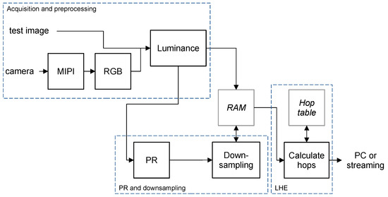
Figure 2.
Block diagram showing the stages of the implementation of LHE, including dependencies with memory (gray blocks in italics) and processing stages.
The first block (MIPI) establishes the connection with the camera and streams the pixels using the MIPI CSI protocol (Mobile Industry Processor Interface and Camera Serial Interface). This block obtains the timing reference signals (beginning of frame, end of line, and pixel valid) and the Bayer values for each pixel. This block is useful when connecting with portable cameras, which in their basic configuration usually provide raw Bayer values. Cameras sense light through a grid of small photosensors, with filters sensitive to green, blue, and red light. These filters are distributed so that 50% of them are green, 25% are blue, and 25% are red, with alternating colors. When raw values are transferred by a camera, they are returned in this special order. Therefore, when a color space used in image processing, such as RGB, is needed, a transform needs to be applied to the data to convert from Bayer values to pixel color values. Although the camera can perform some of this processing, it adds latency to the capture process, the critical first stage. By implementing the transformation process by hand, values can be read faster from the camera, and the heavier computations can be handled by functions that can work with parallelism. The next block (RGB) converts the Bayer raw values into three RGB components per pixel (8 bits each). These blocks were provided by Digilent, Inc. (Pullman, WA, USA) as intellectual property (IP) ready-made blocks for use with their products and set a starting point for processing [29].
The design tested in this work focused on luminance (color intensity) because it carries most of the information from the image and can be used to determine the viability of the system. Following the MIPI and RGB blocks, the luminance block calculates luminance values for each pixel (8 bits, to match other implementations of LHE). To optimize the latency, the following formula with integer coefficients was used:
which corresponds to the studio swing luminance formula from recommendation ITU-R BT.601-7 [30]. These calculations are implemented in hardware with three 16-bit pipelined multipliers, adders, and a right shifter, meaning that data can be processed in a stream as new pixel data arrives. From this point, the data needs to be divided into LHE blocks. For this implementation, the size is . To reduce the need to access memory, each pixel is paired with information about the LHE block to which it belongs. This enables the PR to be calculated for an entire row of LHE blocks without interrupting the streaming. For stages that depend on the PR, the data does need to be stored, so block RAM is dedicated to saving the pixel values while the PR is being processed. The main disadvantage of RAM compared to registers is that only one value can be accessed at a time. In this design, RAM was deemed more suitable as a buffer for repeating the stream of luminance values to other stages, while registers were dedicated to places requiring quick calculations with previous values.
For the PR, and are calculated simultaneously for one line of LHE blocks following the logic in Figure 3. For each horizontal or vertical pair of pixels in a block, the difference is calculated (block DIFF in Figure 3), then quantized. The previous pixels are saved in a register bank (Reg) to calculate the differences. The register bank has a propagation delay of one pixel for the horizontal PR and one line of pixels for the vertical PR. The average of the non-zero differences is then the PR. To obtain the average, one accumulator for the differences and the count of non-zero elements (ACC) and a pipelined divider hardware (÷) are used. The hardware implementation of a divider is a complex circuit, so only two dividers are used for all the blocks in one row (one for each direction). To keep the division error within thousandths of a unit, without significantly impacting the latency, the operations are performed with fixed-point numbers with 10 integer bits and 10 fraction bits (introducing a latency of 20 cycles on the first division). Since the data arrives in a stream and the dividers are pipelined, the calculation of the differences is completed first for the starting block, then for the second block, etc. This allows each block to take turns using the divider. It also means that the next computation stages will start working in a staggered way, which can be exploited for resource sharing.
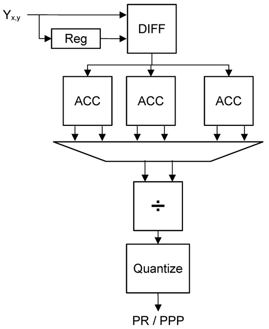
Figure 3.
Block diagram for the implementation of the perceptual relevance (PR block in Figure 2).
Once the PRs have been calculated, the downsampling process can begin. The downsampling components (one per LHE block) read and rewrite data from the previously mentioned RAM. Depending on the PR, the average of 2, 4, or 8 pixels is calculated by adding one pixel and its neighbors. To hold the values of the neighbors as they are added together, delays of one pixel and one line are used in series. Since the dividers are powers of two, a shifter is sufficient to calculate the result. The main problem with variable shifters in hardware is that they may require an additional register bank. Fixed shifters are more efficient because they only require removing bits. The solution adopted for this implementation is to instantiate blocks that accumulate 2, 4, and 8 pixels with fixed shifters. Then, the result is multiplexed according to the PR. The schematic of the proposed architecture is shown in Figure 4.
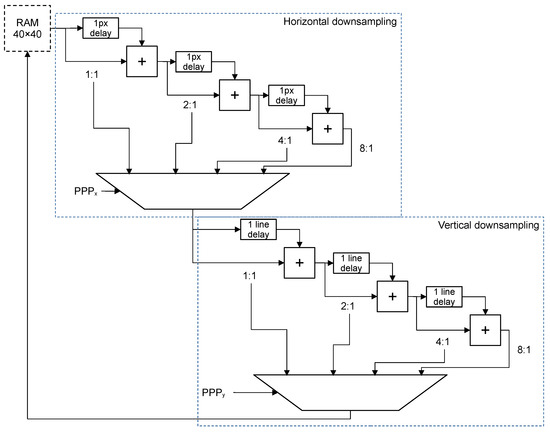
Figure 4.
Block diagram for the implementation of pipelined downsampling (downsampling block in Figure 2).
The last step in the process is the LHE encoding (“Calculate hops” block in Figure 2). The main elements needed for this computation are a table of hop and update values, registers to save pixel values as they are read, and hardware to perform the predictions and calculate intermediate values.
The table with hops and updated values offers a significant advantage in terms of latency and a challenge for resource usage. With a pre-calculated hop table, the most time-consuming part of the algorithm is accelerated. This decision is shared with GPU implementations of the algorithm. However, the size of the table for 8-bit luminance, considering that the cache is symmetrical so half of the range of the original values is omitted, is . This is equivalent to 2688 Kb with 12-bit values, which takes around 20% of the available block RAMs in medium-end FPGAs. For this implementation, only one table was used. This table is shared among all the encoding blocks, which otherwise operate independently. Access to the table is based on the round-robin algorithm.
A prediction based on previous values is calculated for each pixel, so an entire line of pixels is saved in registers. Depending on the pixel’s position relative to the edges of the block, different positions in the pixel register are used to calculate the combinations in Figure 1. As shown in Figure 5, a one-line buffer is enough to access the combinations if the current pixel is not recorded until the calculations are finished. The system always has access to the value of the current pixel (, not yet in the buffer), the previous one in the line (, in the buffer), the one above (, in the buffer and not yet replaced), and the one to the upper-right (, in the buffer). The values of the predictions, which are calculated as the average of the neighbors, are then used as inputs to the hop table, which outputs the hop values. Next, the base value for the first hop and the intermediate gradients are recalculated, which in the case of LHE involves a series of comparisons that can be implemented using multiplexers. After a hop value is produced, the final result from the FPGA is sent for streaming. Because the hop table access is round-robin, pixels from different LHE blocks can often interleave.
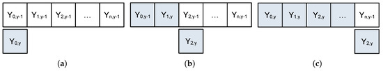
Figure 5.
Access to pixel values in the buffer for the hop prediction for (a) the beginning of the line, (b) the middle of the line, and (c) the last pixel. The upper row shows the buffer and the lower row shows the pixel being currently processed. Pixels in blue belong to the current line (y), and pixels in white belong to the previous line ().
3. FPGA Performance and Validation
Simulations were performed for two distinct implementations of the algorithm using Vivado Simulator (version 2020.2): one optimized with minimal resources for processing resolution images and another for processing images. Functional and timing simulations were conducted for both implementations as these allow for estimation of results and latencies at any internal stage of the processing pipeline on a cycle-by-cycle basis. The latency, maximum clock frequency, and scalability of the design were studied. The obtained results were then compared against those from a GPU implementation of the LHE algorithm designed for embedded devices (e.g., NVIDIA Maxwell GPU). Finally, the FPGA implementation was deployed on a Zybo Z7-20 FPGA connected to an OmniVision OV5640 video camera for real-hardware testing. Code and test programs related to this implementation are available in the GitHub repository linked in the Data Availability Statement.
3.1. Functional Results and Timing
For functional simulations, fixed frames with two resolutions, and , were used as an input to the encoding pipeline. The goal is to test the algorithm under different, controllable scenarios. Three scenarios with different PR were used. Figure 6 shows one LHE block for each scenario. The three scenarios are
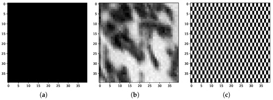
Figure 6.
-pixel LHE blocks belonging to the images of the three different test scenarios: (a) a plain background, (b) a part of a test video frame, and (c) a checkered pattern.
- A single-colored background (“Plain”): this scenario has the lowest possible PR and therefore the highest level of downsampling (8:1) and the lowest amount of hops to calculate.
- An image of leaves from the NTIA test suite [31] (“test”): this scenario has blocks with different PRs and produces an intermediate amount of hops.
- A checkered pattern (“Checkered”): this scenario has alternating color values for each pixel; thus, the PR is maximum. This produces the lowest possible level of downsampling (2:1) and the largest number of hops.
The plain and checkered scenarios are generated in hardware using the pixel synchronization signals. The test scenario uses block RAM to store the image.
A common test bench was written in VHDL connecting a test image generator and the processing blocks (the “PR and downsampling” and “LHE” stages in Figure 2). This test bench resets the design and generates the timing needed for the image generator, then generates timing diagrams with a 150 MHz clock, the same as the one used for real hardware.
The behavior of the camera was incorporated into the simulation by including the timing characteristics of the image transmission. To check that the timing matched that of the real MIPI camera, Vivado’s ChipScope feature, an on-chip debugger, was used to record the camera’s control signals during use. The camera transmits raster lines of RGB values for each pixel. The timing for each line corresponds to the resolution (for a image that would be 69.4 s, while for it would be 46.3 s). Each pixel is transmitted from the camera with a 150 MHz clock (6.6 ns per pixel), accompanied by a “valid” flag. A delay between the second-to-last pixel and the last pixel occurs to synchronize the timing with the end of the line. This allows calculations for most parallel components to start as soon as the first pixel has arrived, but the very last component will have a noticeable delay. For the sake of clarity in the presentation of the results, the latencies of the RGB and luminance stages were not included in the simulation (see Figure 7). However, these latencies are fixed: the RGB block takes four clock cycles according to its documentation [32], and the luminance block takes five cycles. With a 150 MHz clock, this is equivalent to 60 ns, which is negligible compared to the results presented below.
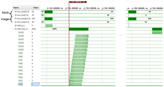
Figure 7.
Example of a simulated timing diagram for the plain image at .
After running the test benches, timing diagrams such as the one shown in Figure 7 were obtained. The delay between most of the blocks’ PRs (marked by the “valid_pr_i” signal in the simulation) and the last block’s PR can be seen in the timing diagram. It can also be observed how the round-robin access to the hop memory makes the hop valid signals (“valid_hop_row” 0–15) appear interleaved.
The latencies measured from the beginning of the image to the first hop and to the last hop of a row of LHE blocks can be seen in Table 2. Since the implementation is pipelined, the sooner the first LHE block is available, the sooner the first hops will be calculated. This means that larger resolutions, where each pixel arrives to the pipeline faster, will have smaller latencies to the first hop. For example, a video line for a image at 30 fps takes 69.4 s to transfer from the camera to the FPGA, while for it takes 46.3 s. Assuming LHE blocks, the first LHE block for a image is fully transferred after 2.7 ms, and for it is transferred after 1.8 ms as more lines to transmit means that the lines need to be transferred faster from the camera. Processing a whole frame takes longer with a larger resolution, but the data can begin to be streamed earlier.
Table 2.
Latency to first and last hop of an LHE row for LHE blocks.
The FPGA implementation discussed thus far does not account for compression algorithms that can be executed before streaming, like entropic coding. However, an estimate of the amount of information to be sent can still be calculated, knowing that each hop in the range [−4, 4] can be encoded using 4 bits. Compression ratios were calculated for full frames based on the three test cases, counting 8 bits per pixel for the original luminance, and 4 bits per hop. These results are presented in Table 3.
Table 3.
Comparison of compression ratios for different test cases.
3.2. Resource Utilization of the Design
To analyze the areas and resource and power utilization of the design, Vivado was set to synthesize and route the design for two different FPGAs in the Zynq series. Constraints for the clock frequency and internal bus clocks were manually configured using Vivado’s Clocking Wizard. Since some IP blocks employ an AXI-Stream interface, additional VHDL code was included to ensure proper integration with Vivado. Furthermore, power estimations and resource utilization metrics were obtained from the reports automatically generated by the Implemented Design Analyzer. To test the design’s scalability, different FPGA models were tested to find the lowest-range model for each resolution. The design for fits on a 7z020clg400-1 FPGA, while the resolution fits on a 7z030fbg484-1 FPGA, the next in the range. The results for the utilization of memories and logic elements including the block RAM used to store the test image can be seen in Table 4. Figure 8 shows a graphical representation of the area used by the different processing blocks inside the FPGAs.
Table 4.
Resource utilization for the LHE design for different image resolutions.
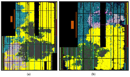
Figure 8.
Layout of the processing blocks in the FPGAs for the LHE design for the resolutions (a) and (b) . The diagonal pattern represents the PR blocks, uniform yellow represents the downsampling blocks, the hatched pattern represents the hops computation blocks, and uniform dark blue represents other regions of the FPGA.
Additionally, Vivado was used to estimate the FPGA’s power consumption given the current design. The results can be found in Table 5.
Table 5.
Estimated power consumption for different image resolutions and FPGA models.
3.3. Comparison to a GPU Implementation
An implementation of the LHE algorithm that targets GPUs was created to serve as a reference benchmark for the FPGA implementation. Since the main objective of this version of the algorithm is to be embedded, the implementation was optimized and tested on a Jetson Nano platform from NVIDIA (Santa Clara, CA, USA) [33]. The Jetson Nano is a single-board computer that includes an embedded NVIDIA Maxwell GPU with 128 CUDA cores and an ARM Cortex-A57 MPCore processor, enabling portable video processing. The GPU version follows the same processing stages for the algorithm, but due to the different architecture and design philosophy of the system, the following changes are present:
- Processing of a frame cannot start until a full frame is transmitted from the camera to the GPU memory. The frame is then processed in its entirety, but that initial latency is present.
- Parallelization occurs at LHE block and line levels, rather than pipelining. One execution thread is dedicated to processing one line, or one column during the PR, downsampling, and hop encoding stages.
- Execution of the stages is fully sequential, that is, one stage cannot start until the previous one has finished.
When executing this implementation with the GPU running on mains power (hence, with the maximum available power), a latency of 13.9 ms is obtained, including the capture time and the transfer from GPU memory to CPU main memory. The latencies of all the intermediate steps are shown in Table 6. Note that measuring the intermediate times introduces a delay, which would explain the difference between the sum of the intermediate contributions and the total measured time. Regarding power consumption, the Jetson Nano board has two power modes [34]: 5 W for battery powered applications and 10 W for other applications. The latencies of Table 6 correspond to the higher performance mode (thus, also to the higher power consumption).
Table 6.
Latency for all the processing stages for a GPU implementation.
3.4. Lab Test with Video Capture
For real hardware tests, a Zybo Z7-20 development board was paired with an external camera, a Pcam 5C from Digilent, Inc. [35]. This module includes an OmniVision OV5640, a 5-megapixel video camera that supports video transmission at different resolutions and frame rates up to QSXGA at 15 fps and interacts out of the box with the MIPI and RGB blocks described earlier. Once the camera is activated, it takes pictures at the desired frame rate, stores them in an internal buffer and begins streaming them in series, transmitting the Bayer values sequentially. The streaming starts in the upper left corner of the frame and rasters the picture line by line. The camera uses control signals to identify the beginning of a frame and the end of a line.
With this setup, validation of the values of the hops was carried out transmitting from a fixed image (the “test” image inserted in block memory inside the design) and a live image (captured with the Pcam 5C pointing at a series of objects). The camera was connected to the FPGA board via the CSI ribbon cable. The manufacturer provides routing inside the board to connect the physical interface to the FPGA proper, ensuring data integrity and pin specifications for Vivado in order to connect the correct pin numbers to the MIPI blocks.
The hop values, as obtained from the FPGA, were transmitted to a PC via a serial connection where a software LHE decoder was run. This software decoder was shared with the GPU implementation. Due to memory limitations, only one row of blocks was transmitted. Figure 9 shows a comparison between the first row of the test image and the image decoded from hops, which keeps a structural similarity of 0.7287 with the original luminance. The LHE decoder adds a border filter to smooth transitions, hence the gray line that appears in the lower border of the image. Figure 10 shows an example of an image captured from the camera. The text (where there is more detail) is compressed at the lowest possible rate, and the background is compressed more.
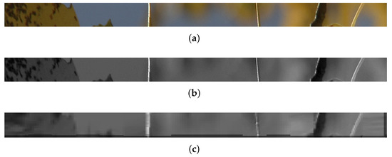
Figure 9.
Comparison between (a) the original color “test” image, (b) the luminance, and (c) the encoded and then decoded version for a row of LHE blocks.

Figure 10.
Example of a decoded image obtained with a camera.
4. Discussion and Conclusions
This work presents an efficient implementation of the LHE algorithm for image processing on FPGAs, specifically designed for embedded systems. We detail the pipeline architecture, starting with the MIPI and RGB blocks for camera interfacing and color space conversion, followed by a dedicated luminance block that utilizes an optimized formula for 8-bit luminance calculation. A key feature of the process is its efficient handling of perceptual relevance calculations and subsequent downsampling, which leverage pipelined architectures and optimized memory access to minimize latency. Furthermore, the LHE encoding stage incorporates a precalculated hop table, offering significant acceleration, albeit with a notable impact on block RAM utilization, which was carefully managed through a shared access scheme.
Our experimental evaluation encompassed simulations using Vivado, targeting two common resolutions in embedded systems ( and ) across a diverse set of image scenarios (plain, test, and checkered patterns) to assess the functional and timing performance. We analyzed the latency, resource utilization (logic slices, RAM blocks, DSPs), and estimated power consumption for the developed FPGA designs, and we compared the results with those of a GPU-based LHE implementation. Finally, we conducted hardware validation by implementing the design on a (Digilent) Zybo Z7-20 board, connecting it to an OmniVision OV5640 camera (OmniVision Technologies, Inc., Santa Clara, CA, USA), and verifying the decoded image quality against both simulated and live captured data.
The simulation results demonstrate an important advantage of the pipelined design in timing, together with a trade-off with throughput and area. The higher the resolution, the sooner the data will be available for processing, and the smaller the latency for both the first and last hops of the block row. As it can be seen in the simulation screenshot in Figure 7, the processing of the perceptual relevance of the next block row can begin while the last hops of the previous row are being processed, so the latencies in Table 2 should also hold up to the last row of the frame. Provided that the streamer reads or buffers the hops at an adequate speed, the latency for a full frame (with the highest PR) would also be 2.92 ms (for ) or 2.1 ms (for ), measured from the starting pixel of the last row of blocks.
These latencies can be compared to those in other papers focusing on parallel and low-latency video codecs. For instance, Mody et al. [36] propose an architecture based on a Texas Instruments DSP system-on-a-chip for HEVC and H.264 encoding with a latency of 2 ms, counting from the end of the frame. In their paper, they point out that typical encoders need a latency of a full frame (33 ms) if the encoding is not run in parallel with image capture. Stabernack and Steinert [37] implemented an H.264 codec in an FPGA using input and output buffers. They report a latency for video of ms, where is related to the image transfer rate, as well as a 0.47 ms latency for the encoding stage (homologous to the downsampling and hop stages). Encoding times are sometimes not reported in the literature, with numbers of frames processed per second given instead. Papers cited in [13] for achieving a low latency, like Tu et al. [38], Sjovall et al. [39], and Yang et al. [40], typically report frame rates of 30 fps to 120 fps, equivalent to 33.3 ms to 8.3 ms per frame. Some of them are as low as 2 ms per frame. These numbers include the entire the processing pipeline, so it is sometimes not possible to isolate the encoding times for different stages. The LHE implementation presented in this paper can be considered competitive in terms of time. In terms of resources, other encoder implementations tend to use more DSP blocks or rely on external RAM for image transfer, while this paper’s proposal relies more on integer or fixed-point calculations and local block RAM.
The clock used for the design is 150 MHz to match that required for the camera. The efficiency of the clock impacts this design in two ways: one is the calculation of the PR, which is performed as the data is streaming, and the other is the downsampling and hop calculation, which depend on a memory buffer (dissociated from the camera, as seen in the schematic in Figure 2). The latency of the PR calculation could be slightly improved with a faster clock due to the latency of the luminance multipliers or that of the PR dividers (Figure 3), but the impact would not be that significant. The multipliers have a latency of three cycles and the dividers, 20 clock cycles, which represent 153.3 ns for this clock, compared with line latencies in the order of tens of microseconds. The downsampling and hop phases could benefit from a faster clock to reduce the PR-to-first hop latency from approximately 10 s, but that could also mean that hops would be produced faster (which in turn calls for a faster readout or buffering mechanism for the streaming phase). In general, pairing a fast-clocked CPU for streaming with a slower clock for LHE can achieve a balance of latency and responsiveness.
Regarding the design’s resource usage, as seen in the layouts and resource counts presented (Figure 8 and Table 4), the system uses a significant percentage of logic and memory. This can be attributed to the use of registers and buffers needed to synchronize operations that depend on previous pixel values. This reduces the processing latency at the cost of more memory. This is particularly evident in the area taken by the downsampling module. Another design option would have been to use the pixel block RAM to write temporary results and replace the one-line delays in Figure 4. This would mean that the horizontal and vertical downsampling stages could not be pipelined, with the consequent increase in latency. By making most of the design rely on integer operations and minimizing the use of multiplications and divisions by a number that is not a power of 2, access to DSP blocks was kept very low.
Compared to the GPU implementation of the algorithm, and excluding memory transfer time, our solution achieves a speedup of 6.61 for resolution (see Table 2 and Table 6). This comes with a 3.7x power reduction (2.7 W vs. 10 W). The FPGA’s power consumption is approximately half of the embedded GPU’s minimum power draw (5 W), making it a far more suitable and efficient choice for battery-powered embedded systems.
This design contributes to the field of real-time video processing by demonstrating an effective method for resource reuse and latency reduction through sub-frame encoding. Its low power consumption and minimal integrated circuit requirements make this approach ideal for low-power, embedded computers. As a result, this design technique is particularly attractive for environments such as unmanned vehicles and portable video systems, where high-end microprocessors or dedicated video cards are not available.
Future work will focus on enhancing several areas in the system’s performance and functionality. The current design only processes the luminance component of the video stream. In future work, we plan to extend the implementation to support full color by incorporating chrominance channels. We also plan to fully characterize the effects of the streamer on latency and bandwidth when integrated with the encoding hardware. Additional points of interest include exploring the impact on latency of other downsampling schemes and validating more efficient data transfer protocols for decoding or streaming the output to a PC.
Author Contributions
Conceptualization, J.J.A.; methodology, J.J.A., A.O. and P.P.-T.; software, for GPU J.J.A., M.A.G., F.J.J.Q., for FPGA P.P.-T.; validation, P.P.-T. and J.J.A.; investigation, P.P.-T.; resources, J.J.A. and G.C.; writing—original draft preparation, P.P.-T.; writing—review and editing, A.O.; visualization, P.P.-T.; supervision, A.O., J.J.A. and G.C.; project administration, J.J.A.; funding acquisition, J.J.A. All authors have read and agreed to the published version of the manuscript.
Funding
This research was funded by the Spanish Ministry of Science, Innovation and University through the CDTI project FLYINGDRONES IDI-20210468.
Institutional Review Board Statement
Not applicable.
Informed Consent Statement
Not applicable.
Data Availability Statement
The code for the system described in this paper is publicly available in the following GitHub repository: https://github.com/ppereztirador/flyingdrones-fpga (updated 22 September 2025).
Conflicts of Interest
Authors Jose Javier Aranda, Manuel Alarcon Granero, and Francisco J. J. Quintanilla were employed by the company Nokia Spain, SA. The remaining authors declare that the research was conducted in the absence of any commercial or financial relationships that could be construed as potential conflicts of interest. The sponsors had no role in the design of the study; in the collection, analysis, or interpretation of the data; in the writing of the manuscript; or in the decision to publish the results.
Abbreviations
The following abbreviations are used in this manuscript:
| CSI | Camera Serial Interface |
| DSP | Digital Signal Processor |
| FPGA | Field-Programmable Gate Array |
| fps | Frames Per Second |
| GPU | Graphics Processing Unit |
| LHE | Logarithmic Hop Encoding |
| MIPI | Mobile Industry Processor Interface |
| PPP | Plane Predicted Pixel value |
References
- Florez, R.; Palomino-Quispe, F.; Alvarez, A.B.; Coaquira-Castillo, R.J.; Herrera-Levano, J.C. A Real-Time Embedded System for Driver Drowsiness Detection Based on Visual Analysis of the Eyes and Mouth Using Convolutional Neural Network and Mouth Aspect Ratio. Sensors 2024, 24, 6261. [Google Scholar] [CrossRef]
- Marwedel, P. Embedded System Design: Embedded Systems Foundations of Cyber-Physical Systems, and the Internet of Things; Springer Nature: Berlin/Heidelberg, Germany, 2021. [Google Scholar]
- Almeida, L.; Menezes, P.; Dias, J. Telepresence social robotics towards co-presence: A review. Appl. Sci. 2022, 12, 5557. [Google Scholar] [CrossRef]
- Kangunde, V.; Jamisola Jr, R.S.; Theophilus, E.K. A review on drones controlled in real-time. Int. J. Dyn. Control 2021, 9, 1832–1846. [Google Scholar] [CrossRef]
- Mademlis, I.; Symeonidis, C.; Tefas, A.; Pitas, I. Vision-based drone control for autonomous UAV cinematography. Multimed. Tools Appl. 2024, 83, 25055–25083. [Google Scholar] [CrossRef]
- Kai, Y.; Seki, Y.; Suzuki, R.; Kogawa, A.; Tanioka, R.; Osaka, K.; Zhao, Y.; Tanioka, T. Evaluation of a Remote-Controlled Drone System for Bedridden Patients Using Their Eyes Based on Clinical Experiment. Technologies 2023, 11, 15. [Google Scholar] [CrossRef]
- Luo, H.; Wang, X.; Bu, F.; Yang, Y.; Ruby, R.; Wu, K. Underwater real-time video transmission via wireless optical channels with swarms of auvs. IEEE Trans. Veh. Technol. 2023, 72, 14688–14703. [Google Scholar] [CrossRef]
- Behiry, A.A.M.R.; Dafar, T.; Hassan, A.E.M.; Hassan, F.; AlGohary, A.; Khanafer, M. Nu—A Marine Life Monitoring and Exploration Submarine System. Technologies 2025, 13, 41. [Google Scholar] [CrossRef]
- Liu, Z.; Hu, C.; Wang, B.; Chen, J.; Deng, S.; Yu, J. A minimizing energy consumption scheme for real-time embedded system based on metaheuristic optimization. IEEE Trans. Comput.-Aided Des. Integr. Circuits Syst. 2022, 42, 2276–2289. [Google Scholar] [CrossRef]
- Bray, N.; Boeding, M.; Hempel, M.; Sharif, H.; Heikkilä, T.; Suomalainen, M.; Seppälä, T. A latency composition analysis for telerobotic performance insights across various network scenarios. Future Internet 2024, 16, 457. [Google Scholar] [CrossRef]
- Black, D.G.; Andjelic, D.; Salcudean, S.E. Evaluation of communication and human response latency for (human) teleoperation. IEEE Trans. Med. Robot. Bionics 2024, 6, 53–63. [Google Scholar] [CrossRef]
- Hong, D.; Lee, S.; Cho, Y.H.; Baek, D.; Kim, J.; Chang, N. Energy-efficient online path planning of multiple drones using reinforcement learning. IEEE Trans. Veh. Technol. 2021, 70, 9725–9740. [Google Scholar] [CrossRef]
- Žádník, J.; Mäkitalo, M.; Vanne, J.; Jääskeläinen, P. Image and Video Coding Techniques for Ultra-low Latency. ACM Comput. Surv. 2022, 54, 1–35. [Google Scholar] [CrossRef]
- Palau, R.; Silveira, B.; Domanski, R.; Loose, M.; Cerveira, A.; Sampaio, F.; Palomino, D.; Porto, M.; Corrêa, G.; Agostini, L. Modern Video Coding: Methods, Challenges and Systems. J. Integr. Circuits Syst. 2021, 16. [Google Scholar] [CrossRef]
- Kilic, F.; Hassan, M.; Hardt, W. Prototype for Multi-UAV Monitoring–Control System Using WebRTC. Drones 2024, 8, 551. [Google Scholar] [CrossRef]
- Sacoto-Martins, R.; Madeira, J.; Matos-Carvalho, J.P.; Azevedo, F.; Campos, L.M. Multi-purpose Low Latency Streaming Using Unmanned Aerial Vehicles. In Proceedings of the 2020 12th International Symposium on Communication Systems, Networks and Digital Signal Processing (CSNDSP), Porto, Portugal, 20–22 July 2020; pp. 1–6. [Google Scholar] [CrossRef]
- Baltaci, A.; Cech, H.; Mohan, N.; Geyer, F.; Bajpai, V.; Ott, J.; Schupke, D. Analyzing real-time video delivery over cellular networks for remote piloting aerial vehicles. In Proceedings of the 22nd ACM Internet Measurement Conference, New York, NY, USA, 25–27 October 2022; IMC ’22. pp. 98–112. [Google Scholar] [CrossRef]
- García Aranda, J.J.; González Casquete, M.; Cao Cueto, M.; Navarro Salmerón, J.; González Vidal, F. Logarithmical hopping encoding: A low computational complexity algorithm for image compression. IET Image Process. 2015, 9, 643–651. [Google Scholar] [CrossRef]
- García Aranda, J.J.; Alarcón Granero, M.; Juan Quintanilla, F.J.; Caffarena, G.; García-Carmona, R. Elastic downsampling: An adaptive downsampling technique to preserve image quality. Electronics 2021, 10, 400. [Google Scholar] [CrossRef]
- Seng, K.P.; Lee, P.J.; Ang, L.M. Embedded intelligence on FPGA: Survey, applications and challenges. Electronics 2021, 10, 895. [Google Scholar] [CrossRef]
- Desai, M.P.; Caffarena, G.; Jevtic, R.; Márquez, D.G.; Otero, A. A low-latency, low-power FPGA implementation of ECG signal characterization using hermite polynomials. Electronics 2021, 10, 2324. [Google Scholar] [CrossRef]
- Prabakaran, G.; Vaithiyanathan, D.; Ganesan, M. FPGA based intelligent embedded system for predicting the productivity using fuzzy logic. Sustain. Comput. Inform. Syst. 2022, 35, 100749. [Google Scholar] [CrossRef]
- Kövari, B.B.; Ebeid, E. MPDrone: FPGA-based platform for intelligent real-time autonomous drone operations. In Proceedings of the 2021 IEEE International Symposium on Safety, Security, and Rescue Robotics (SSRR), New York, NY, USA, 25–27 October 2021; pp. 71–76. [Google Scholar]
- Chen, C.; Min, H.; Peng, Y.; Yang, Y.; Wang, Z. An intelligent real-time object detection system on drones. Appl. Sci. 2022, 12, 10227. [Google Scholar] [CrossRef]
- Perez-Tirador, P.; Jevtic, R.; Cabezaolias, C.; Romero, T.; Otero, A.; Caffarena, G. The effect of ECG data variability on side-channel attack success rate in wearable devices. Integration 2025, 103, 102385. [Google Scholar] [CrossRef]
- Sudhakar, K.; PIRAJIN, S.S.; Shanmugapriyan, J.; Sujeeth, S. Design and Implementation of FPGA based Rescue Bot. In Proceedings of the 2023 7th International Conference on Computing Methodologies and Communication (ICCMC), Erode, India, 23–25 February 2023; pp. 1636–1643. [Google Scholar]
- Wang, W.; Chen, Z.; Yuan, X. Simple low-light image enhancement based on Weber–Fechner law in logarithmic space. Signal Process. Image Commun. 2022, 106, 116742. [Google Scholar] [CrossRef]
- Digilent, Inc. Zybo Z7-20 Reference Manual. Available online: https://digilent.com/reference/programmable-logic/zybo-z7/reference-manual (accessed on 23 July 2025).
- Digilent, Inc. GitHub Repository for IP. Available online: https://github.com/Digilent/vivado-library/ (accessed on 30 July 2025).
- Studio Encoding Parameters of Digital Television for Standard 4:3 and Wide Screen 16:9 Aspect Ratios; Rec. ITU-R BT.601-7; International Telecommunications Union: Geneva, Switzerland, 2011.
- Pinson, M.H.; Schmidmer, C.; Janowski, L.; Pépion, R.; Huynh-Thu, Q.; Corriveau, P.; Younkin, A.; Le Callet, P.; Barkowsky, M.; Ingram, W. Subjective and objective evaluation of an audiovisual subjective dataset for research and development. In Proceedings of the 2013 Fifth International Workshop on Quality of Multimedia Experience (QoMEX), Klagenfurt am Wörthersee, Austria, 3–5 July 2013; pp. 30–31. [Google Scholar] [CrossRef]
- Digilent, Inc. GitHub, Code for AXI_BayerToRGB.vhd. Available online: https://github.com/Digilent/Zybo-Z7-20-pcam-5c/blob/master/repo/local/ip/AXI_BayerToRGB/hdl/AXI_BayerToRGB.vhd (accessed on 30 July 2025).
- Nvidia Jetson Nano. Available online: https://developer.nvidia.com/embedded/jetson-nano (accessed on 30 July 2025).
- Jetson Nano 2GB Developer Kit User Guide. Available online: https://developer.nvidia.com/embedded/learn/jetson-nano-2gb-devkit-user-guide (accessed on 30 July 2025).
- Digilent, Inc. Pcam 5C Reference Manual. Available online: https://digilent.com/reference/add-ons/pcam-5c/reference-manual (accessed on 23 July 2025).
- Mody, M.; Swami, P.; Shastry, P. Ultra-low latency video codec for video conferencing. In Proceedings of the 2014 IEEE International Conference on Electronics, Computing and Communication Technologies (CONECCT), Bangalore, India, 6–7 January 2014; pp. 1–5. [Google Scholar] [CrossRef]
- Stabernack, B.; Steinert, F. Architecture of a Low Latency H.264/AVC Video Codec for robust ML based Image Classification. In Proceedings of the Workshop on Design and Architectures for Signal and Image Processing, 14th ed.; Association for Computing Machinery: New York, NY, USA, 2021; DASIP ’21; pp. 1–9. [Google Scholar] [CrossRef]
- Tu, J.S.; Lin, K.S.; Lin, C.L.; Kao, J.Y.; Shih, G.R.; Tsai, P.H. Low-latency implementation of 360 panoramic video viewing system. In Proceedings of the 2017 International Symposium on Intelligent Signal Processing and Communication Systems (ISPACS), Xiamen, China, 6–9 November 2017; pp. 576–579. [Google Scholar] [CrossRef]
- Sjövall, P.; Viitamäki, V.; Vanne, J.; Hämäläinen, T.D.; Kulmala, A. FPGA-powered 4K120p HEVC intra encoder. In Proceedings of the 2018 IEEE International Symposium on Circuits and Systems (ISCAS), Florence, Italy, 27–30 May 2018; pp. 1–5. [Google Scholar] [CrossRef]
- Yang, S.; Li, B.; Song, Y.; Xu, J.; Lu, Y. A hardware-accelerated system for high resolution real-time screen sharing. IEEE Trans. Circuits Syst. Video Technol. 2018, 29, 881–891. [Google Scholar] [CrossRef]


Disclaimer/Publisher’s Note: The statements, opinions and data contained in all publications are solely those of the individual author(s) and contributor(s) and not of MDPI and/or the editor(s). MDPI and/or the editor(s) disclaim responsibility for any injury to people or property resulting from any ideas, methods, instructions or products referred to in the content. |
© 2025 by the authors. Licensee MDPI, Basel, Switzerland. This article is an open access article distributed under the terms and conditions of the Creative Commons Attribution (CC BY) license (https://creativecommons.org/licenses/by/4.0/).