1. Introduction
The onset of Very Large-Scale Integration (VLSI) has led to the advent of chips designed to perform a particular operation, resulting in the emergence of Application-Specific Integrated Circuits (ASIC) designs. Mastering the ASIC design process in digital VLSI is the cornerstone to successfully designing chips. The advent of sophisticated processing nodes has ushered in a new era of increased transistor density and given rise to complex and power-efficient ASICs. ASIC design engineers have consistently tried to break the barriers in the ever-evolving realm of VLSI design by adopting emerging trends and exploiting cutting-edge technological innovations.
The arithmetic computational unit is an indispensable part of processors suited to image and signal processing applications. Several commercial processors have emerged as a result of the broadening of Digital Image Processing (DIP) applications. These processors have efficient computational units that boost overall performance, paving the way for faster and low-power computing. Extensive recurrent mathematical computations are required for these operations, resulting in increased delay and power consumption. High-speed computational units with low power consumption are desired for high performance in digital image and signal processing applications. The advent of emerging technologies and device scaling demands computational units to be constructed with lower power consumption, less propagation delays, and reduced dimensions.
The computational unit’s architectural design and efficiency are deciding factors for the speed and power of the Central Processing Unit (CPU). This research explores different adder and multiplier architecture designs by incorporating low-power techniques and implements the computational unit design that is most suitable for DIP applications. The proposed computational unit comprises an Error-Tolerant (ET) adder, a Power Delay Product (PDP) optimized fixed-point multiplier, and a low-power logical unit. This research presents the design, development, and implementation of a PDP optimized ASIC-based computational unit for image processing applications.
Through the low-power concept of approximate computing, an ET adder is implemented in this research, which significantly improves both performance and power at the expense of accuracy. Multipliers form an indispensable part of almost all high-speed processors and CPUs, as a result of which research on the low-power design of multipliers makes a significant contribution to society. There is a rapid surge in the market demand for compact and lightweight electronic devices. An apparent low power demand emerges from such advanced forces of electronic circuits. Clock frequencies have been increasing for higher performance. Faster circuits are required to work at high clock frequencies, which increases the chip complexity, power consumption, and area. This has led to innovative techniques of low-power VLSI. The frequency has been limited to 4.5 GHz due to power limitations [
1].
If the power consumption can be reduced with an acceptable increase in delay, then the frequencies can be increased, which is the necessity of high-performance devices, especially mobile phones. PDP optimized multipliers and arithmetic units are essential. The image processing algorithms implemented in contemporary times with software techniques are slower due to the limitations imposed by the processor’s speed. A dedicated computational unit is necessary for image processing implementations to keep up with the speeds of high-performance applications operating at high clock frequencies. Due to the limitations imposed by General-Purpose Processors (GPP), implementing image processing algorithms in real time is complex as it requires high computational power and throughput rate. ASICs are suitable for stand-alone image processing applications due to their small size, lower power consumption, and greater functionality when used for specific purposes. ASICs can be customized to implement specific algorithms in a single small-sized, low-power integrated circuit, unlike GPP [
1].
The computational units designed for image and signal processing applications comprise adders, multipliers, and logical units to perform various computations. A broad range of adder and multiplier architectures were proposed to meet the demands of high-performance devices. Complex tasks were executed in software or micro-code with minimal assistance from hardware during the early years of processor development. A review of the different architectures of Arithmetic Logic Unit (ALU) that were designed in the past to meet the demands of reduced power, area, enhanced efficiency, and high speeds is discussed in this section.
Lachireddy et al. [
2] focused on the design of an ALU using reversible logic to reduce the power and Vedic multiplication to increase the speed. Two multiplier designs were modeled, one using the Vedic multiplier and the other using the Booth multiplier. A drop of 6.7% in dynamic power and a 2.2% reduction in area was observed in the design that used the proposed Vedic algorithm.
Suchismita et al. [
3] presented the design for a custom 4-bit ALU that consumed less power and was fast. The power consumption was lower compared to the designs implemented using conventional techniques. Since different modules were used for each operation, the overall complexity was more in terms of area.
Madhukar et al. [
4] proposed the design of a 16-bit ALU for high-speed and low-power applications. A parallel prefix adder, the Brent Kung adder, was utilized to perform the addition operation as it consumed less power. The multiplication operation was performed using the Booth multiplier, involving fewer additions than the existing array and Wallace multipliers. The restoring algorithm used for division consumed less power than subtractive methods. The design exhibited reduced delay and power consumption at a slightly increased area.
Suhas et al. [
5] designed a hybrid 32-bit ALU using irreversible and reversible gates. The modified Carry Save Adder (CSA) was implemented using reversible gates to reduce the power further. The Urdhva Tiryagbhyam (UT) sutra of Vedic mathematics was used to design the multiplier, and the addition of the partial products was performed using the delay-modified CSA to further reduce the delay. Reversible logic gates were used to design the subtractor. The design exhibited an overall reduction in power and delay but with an increased area. Kamaraj et al. [
6] designed an ALU that was fault-tolerant using KMD, Toffoli, and Fredkin reversible gates, which were functionally realized in Quantum Cellular Automata. A single module performed the arithmetic and logical operations. The design utilizes more gates but with less quantum cost.
Rashmi et al. [
7] implemented two 8-bit ALUs for low-power by incorporating the techniques of clock gating and operand isolation at the Register Transfer Level (RTL) level. Compared to conventional designs, the design with operand isolation showed that it consumed more power and occupied more area with less delay. Similarly, the design with clock gating consumed less power, but the area and delay were more than those of conventional designs. Nagarjuna et al. [
8] proposed a low-power 8-bit ALU with two 4 × 1 data selectors, a 2 × 4 decoder, a full adder, and a logic unit. The design seemed complex in terms of area, as it involved decoders and data selectors.
Maan et al. [
9] compared different clock gating techniques in 8-bit ALUs. The newly proposed technique of achieving clock gating using a tristate buffer resulted in more power and area savings as the idle parts were eliminated. The use of the tristate buffer showed an improved performance. Moresh et al. [
10] presented a 4-bit ALU utilizing the Gate Diffusion Input (GDI) approach. GDI is a novel method to design low-power combinational circuits that reduce power and area. In contrast to conventional designs, the proposed concept was fast and efficient.
Priyanka et al. [
11] suggested an 8-bit ALU with a Knowles adder for addition and a Vedic multiplier constructed using the Ladner-Fisher approach. The multiplier used in the design had better power, area, and delay efficiency than the Vedic multipliers used in conventional designs. The design utilized the Knowles adder to reduce the routing complexity and area. The efficiency of the adder and multiplier used can be further improved.
Abdul et al. [
12] designed two types of architectures of 32-bit ALUs using the Sklansky and Ripple Carry Adder (RCA) adders. In addition, the power and area of the architecture with RCA were compared to those of the architecture constructed without a demultiplexer. This was achieved by employing a demultiplexer to cut off the power to the blocks that were not in use. The results showed that the architecture designed with a demultiplexer proved to be more power-efficient. A power-saving method for an 8-bit ALU utilizing clock gating by incorporating a negative latch was presented by Gunjan et al. [
13]. The design was implemented at the RTL level on an FPGA, and the results of power consumed were compared with a D Flip Flop-based clock gated design (243 mw at 100 MHz), which showed a significant power reduction. The design that used the negative latch exhibited an increased area and speed.
An 8-bit ALU was proposed by Akram et al. [
14] utilizing a method to lower leakage power. The power supply was decreased, and the ground potential was raised to compensate for the delay overhead that lowered the leakage power. Bishwajeet et al. [
15] proposed an ALU of size 8 bits that utilized AND gate-based clock gating to reduce the dynamic and clock power consumed. Power savings were achieved by powering off the inactive modules using the clock gating approach. The analysis of power and area was conducted at different clock frequencies, and it was found that even though there was a reduction in clock and dynamic power, there was an overhead of increased area.
Sushma et al. [
16] have presented a Vedic multiplier by proposing an area and speed-efficient design for an ALU. Unlike conventional designs, the novel Multiplier Adder and Subtractor (MAS) unit was implemented by aggregating the adder, subtractor, and multiplier, thereby reducing the area, and by modifying the UT formula for Vedic multiplication. The MAS-based multiplier proved to be faster than the Booths algorithm but slower than the UT multiplier. The MAS-based multiplier was found to occupy slightly more area than the Urdhva method of multiplication and Booth’s algorithm.
To increase efficiency, M. Kamaraju et al. [
17] presented the design of a 16-bit ALU with lower power consumption that used the clock gating approach. The design was divided into four functional blocks, each designed to perform four operations. Clock gating was achieved using a decoder that generated the coded clock signals based on an opcode to the desired functional block. Power dissipation can be reduced further by using improved techniques for clock gating, and high-speed adders and multipliers can be used to enhance the speed further. Substantial work has been conducted to design ALUs to meet the expectations of high-speed processors. The overall power can be lowered by minimizing the power of the adders and multipliers used in the ALUs.
Medical images like Magnetic resonance imaging (MRI), Computed Tomography (CT) scans, and X-rays in the healthcare domain have an increased size owing to substantial high-resolution information packed into a single image. The processing of these high-resolution images for various applications requires the images to be compressed in size to reduce the memory occupied by these images, especially for applications that demand high speed and less area. Researchers have been consistently working on different algorithms to compress the images. Most of the existing work focused on reducing the size of the images with less emphasis on the computational complexity of the processor. The growing demand for efficient transmission and storage of medical images at a reduced computational complexity in the medical field is the driving force of research designing a computational unit for image compression.
The compression of medical images based on transforms has recently resulted in a huge demand due to their growing applications in the medical domain, attracting researchers. The efficiency and computational speed of Discrete Cosine Transform (DCT) are among the most sought-after algorithms, especially for medical images. Some of the DCT algorithms used in different medical image compression applications are listed here to give a clear idea about the existing work.
An image compression algorithm using DCT was proposed by Wu et al. [
18], and the significant coefficients were obtained using adaptive sampling techniques. The proposed algorithm resulted in compressing the images and preserving the information fidelity. Chen et al. [
19] proposed a Two-Dimensional (2D) image compression method for medical images utilizing DCT and hierarchical tree partitioning. An approach with a reduced bit rate, resulting in minimizing the memory requirement for storing the remote diagnosis and for the rapid transmission, was also adopted in this work.
An approximation technique for 8-point DCT with 14 addition operations utilizing the separability property of DCT was presented by Potluri et al. [
20]. A reduction in the algorithm and computational complexity was observed. Kaur et al. [
21] have proposed context tree lossless compression for the Region Of Interest (ROI) image part and a lossy compression fractal for the non-ROI part of the image. The proposed method provided much faster and more accurate results even though the PSNR was slightly lower.
The research carried out by Suma et al. [
22] focused on the utilization of the UT sutra in the design of the multiplier that was incorporated into the image compression algorithm. A significant reduction in the size of the image was observed with less data loss. The compression speed was improved with the use of the Vedic multiplier as the computation time of the image compression algorithm was reduced. In their work, Liu et al. [
23] discussed the different standards used in image compression, mainly for medical images. A comparison of the performances of the different compression standards on publicly available datasets was also conducted.
A DCT architecture without multipliers was proposed for medical applications targeting capsule endoscopy by Xing et al. [
24]. Approximate adders, threshold setting, and coefficient optimization were incorporated into the DCT algorithm design. A DCT architecture utilizing inexact adders was proposed by Kumar et al. [
25]. Considerable savings in area and power were observed due to the absence of multipliers in the architecture. Hosny et al. [
26] presented a 2D medical image compression algorithm in their work. The algorithm proposed exhibited high compression rates and good image resolution.
Alzahrani et al. [
27], in their work, compared two lossless transforms, DCT and Haar Wavelet Transform (HWT), with medical images in terms of image size and compression ratio. It was observed from their inferences that while using grayscale images, DCT proved to perform much better than HWT. HWT was found to be a better choice when color images were used and in terms of compression time. A discussion on image compression algorithms using DWT and Huffman coding was presented by Mydin et al. [
28] in their work. In their work, Rahman et al. [
29] analyzed and evaluated the strength of different lossless compression techniques based on more than one parameter. In an attempt to improve the compression ratios, the medical image compression techniques discussed resulted in a reduced quality of images and loss of minute details, which is undesirable in medical images.
Medical image compression primarily aims to reduce the image size to minimize the memory required for processing and storing the image without affecting its quality. Even though considerable research strategies for medical image compression were developed, an algorithm specific to medical image compression that focuses on reducing computational speed, area, and power has not been developed.
The digital compression of medical images, especially for telemedicine, has gained significant importance in recent years due to medical advancements. Primary health care, especially in villages, is challenging owing to the limited facilities available and the lack of well-trained health personnel. With telemedicine, most of the problems faced by people living in villages can be solved. The main idea behind telemedicine is the efficient transmission of medical images to healthcare professionals in modern cities. A critical factor that comes into play in telemedicine is to handle the transmission of cumbersome medical images with comparatively lower bandwidth. This demands that the medical images be compressed to enable the efficient and error-free transmission of information. This research explores the DCT that can be utilized for digital image compression by incorporating the computational unit to reduce computational complexity and minimize power as well as area. In the DCT coding technique followed in this research, a considerable set of highly correlated pixels are transformed to a comparatively smaller set of transform coefficients that are decorrelated. The quantization and encoding of the coefficients are then performed to obtain the compressed image.
This research aims to design and develop a computational unit for medical image compression comprising a modified Carry Select Adder (CSLA)-based Selector-Based Error Tolerant Adder (SBETA)/Low-Power Selector-Based Error Tolerant Adder (LPSBETA)/Optimized Error Tolerant Adder (OETA) using RCA, a divide and conquer multiplier, a PDP optimized multiplier using iterative carry save SBETA and a logic unit using operand isolation. In the proposed research work, an architecture of a computational unit incorporated in the Loeffler 8-point DCT/IDCT algorithm and used for medical image compression applications is proposed, designed, and implemented. The ET adders designed using the low-power concept of approximate computing substitute the addition operations involved in Loeffler’s fast algorithm’s DCT/IDCT computations. This reduces the hardware complexity, resulting in significant savings in area and power. The Binary to Excess 1 Converters (BEC) used in the modified CSLA reduces the number of gates involved, leading to lesser power and area as the transitions rely on only one bit. The multiplications involved are minimized by approximating some of the cosine constants involved and using the proposed low-power multipliers and shifters to reduce the computational complexity. An efficient encoding and decoding block is proposed using the improved Loeffler algorithm. The contributions of this research are as follows:
A DCT/IDCT architecture based on the Loeffler algorithm by incorporating the computational unit to perform the additions involved in the butterfly diagram using the ET adders and the low-power multipliers for the multiplications involved.
An improved encoding and decoding block is used to reduce the circuit complexity and improve the compression ratio, SSIM, and PSNR without affecting the quality of the reconstructed image.
An approach to building a computational unit by integrating VLSI ASIC design and the concepts of low-power VLSI compatible for medical image compression used in telemedicine was adopted in this research.
The VLSI ASIC design flow that is followed in this research work is presented in
Section 2.
Section 3 elaborates on the development of the proposed computational unit designed and implemented in this research. The modified CSLA-based SBETA/LPSBETA/OETA using RCA, a divide and conquer multiplier, a PDP optimized multiplier using iterative carry save SBETA, and a logic unit using operand isolation incorporated in the computational unit is also discussed in
Section 3. The digital image compression application using the proposed computational unit for the medical image is demonstrated in the last portion of
Section 3. The results of the proposed computational unit are discussed in
Section 4. The concluding remarks of the research work are given in
Section 5.
2. VLSI ASIC Design Flow
The ASIC design flow comprises several steps, from conceptualization to specification and tape-outs, as shown in
Figure 1. The end product usually is small in the order of nanometers. The ASIC design flow starts with the specification definition of the system [
30].
The current emphasis of low-power VLSI design is on designing and implementing power-efficient algorithms of arithmetic units such as adders, subtractors, multipliers, and dividers. Due to the rapid growth of wireless devices in the electronics market, total power consumption, a core design constraint, must be addressed. The efficient design of an Integrated Circuit (IC), considering low power, high speed, and small area, is quite challenging [
31]. Since maximizing the run time of these portable devices is desirable, reducing power consumption becomes a critical factor that requires careful consideration [
32].
The most demanding constraint when it comes to the design of an efficient, high-performance system in nanometer technologies is power dissipation. ASICs, having optimized performance, offer better power efficiency than other implementation schemes. ASIC offers lower power solutions and higher speeds for the same processor technology due to its interconnect architecture compared to FPGA. Due to the limitations imposed by general-purpose processors regarding computational power and throughput, implementing image processing algorithms in real time is complex as it requires high computational power and throughput rate. ASICs are semiconductors that can be specially designed for a particular function. They can reduce silicon area with high efficiency in speed and power, making them suitable candidates for image processing applications.
The efficient implementation of the different arithmetic circuits of the computational unit for executing distinct algorithms is realizable with ASIC. As the complexity of arithmetic circuits increases, so does the power consumption and transistor density, giving rise to the low-power design techniques of VLSI with state-of-the-art concepts. With the ever-growing popularity of battery-powered electronic devices, area, power, and delay from the perspective of a circuit play a significant part in VLSI. As the area increases, the number of logic gates also increases, slowing the circuit and increasing power consumption. A trade-off often exists among power, delay, and area in VLSI.
The PDP is the design metric that gauges the effectiveness and performance of low-power devices. As the complexity of the devices increases, the power dissipation keeps rising, impacting the performance and reliability. In such a scenario, power consumption becomes an integral part of the design that requires the design constraints to be further optimized. The latest technological advancements have led researchers to work to design power-efficient, high-speed, and smaller devices with a focus on Power Delay Area (PDA) constraints.
3. Development of the Proposed Computational Unit
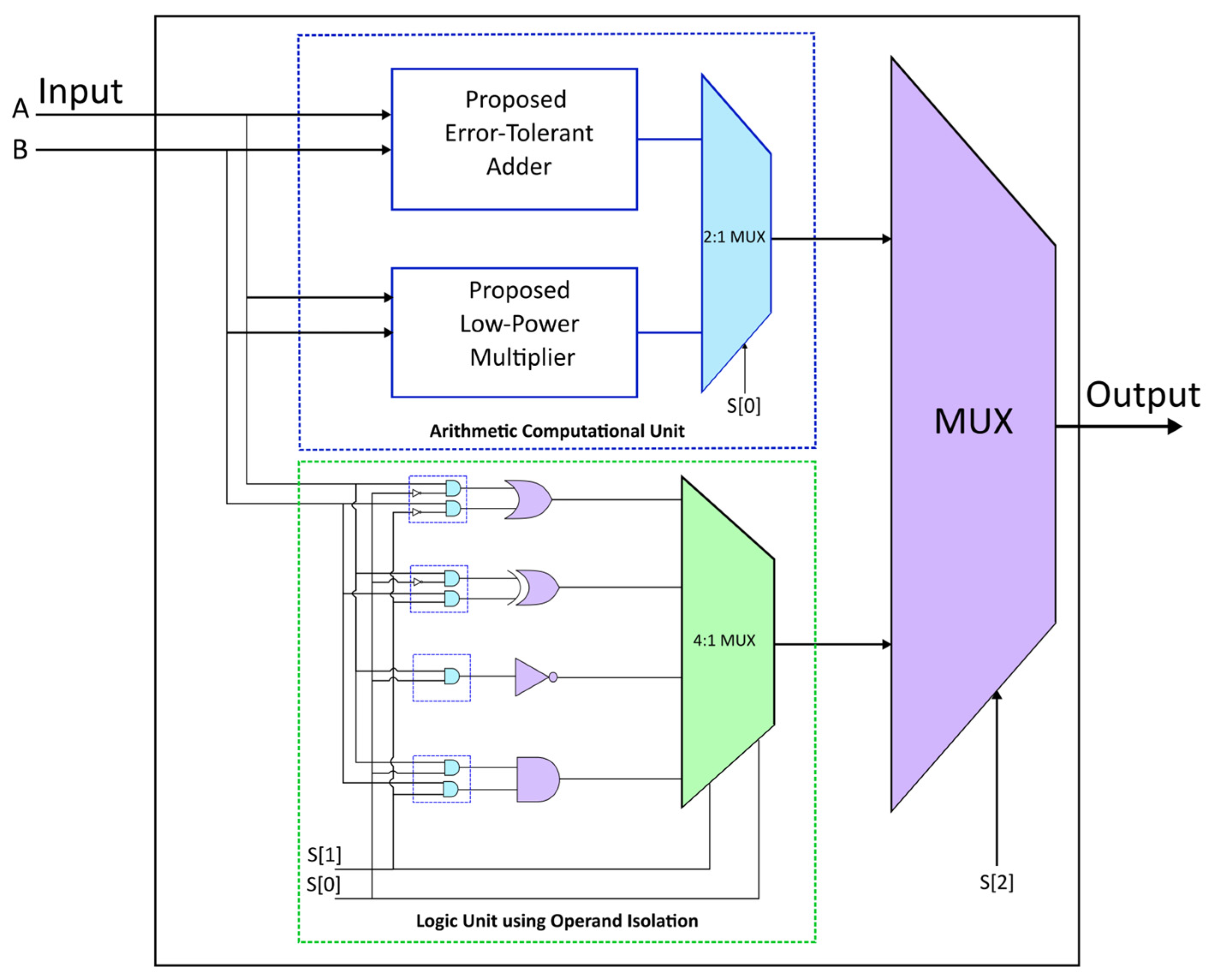
A universal integrated logic device, the computational unit performs arithmetic and logical computations. The computational unit is an essential microprocessor component due to its versatility. The computational unit proposed in this research is illustrated using the block diagram shown in
Figure 2. The computational unit takes two operands, A and B, as inputs and produces an output by applying predefined operations to the inputs, as presented in
Table 1. The selection input S(2) decides the arithmetic or logic operation. The inputs S(1) and S(2) decide the operations to perform within the arithmetic or logic block. The arithmetic computational unit comprises an ET adder and a low-power multiplier. An OR, AND, XOR, and NOT logical gate comprises the logic unit using operand isolation.
The computational unit is built by integrating the ET adders, the low-power multipliers, and the logic unit for 8-bit, 16-bit, and 32-bit computations. The computational unit has been configured so that the logical module activates when S(2) is 1, and the arithmetic module activates when the select input S(2) is 0. Depending on the S(0) input, addition using the ET adders or multiplication utilizing the low-power multipliers is performed. When the input S(2) is 1, the inputs S(1) and S(0) determine which logical operation has to be carried out. The different combinations of designs are mentioned in
Table 2.
3.1. Modified CSLA-Based Adders Using Error Tolerant Adders
The arithmetic computations are accomplished utilizing the ET Adders presented in our previous research [
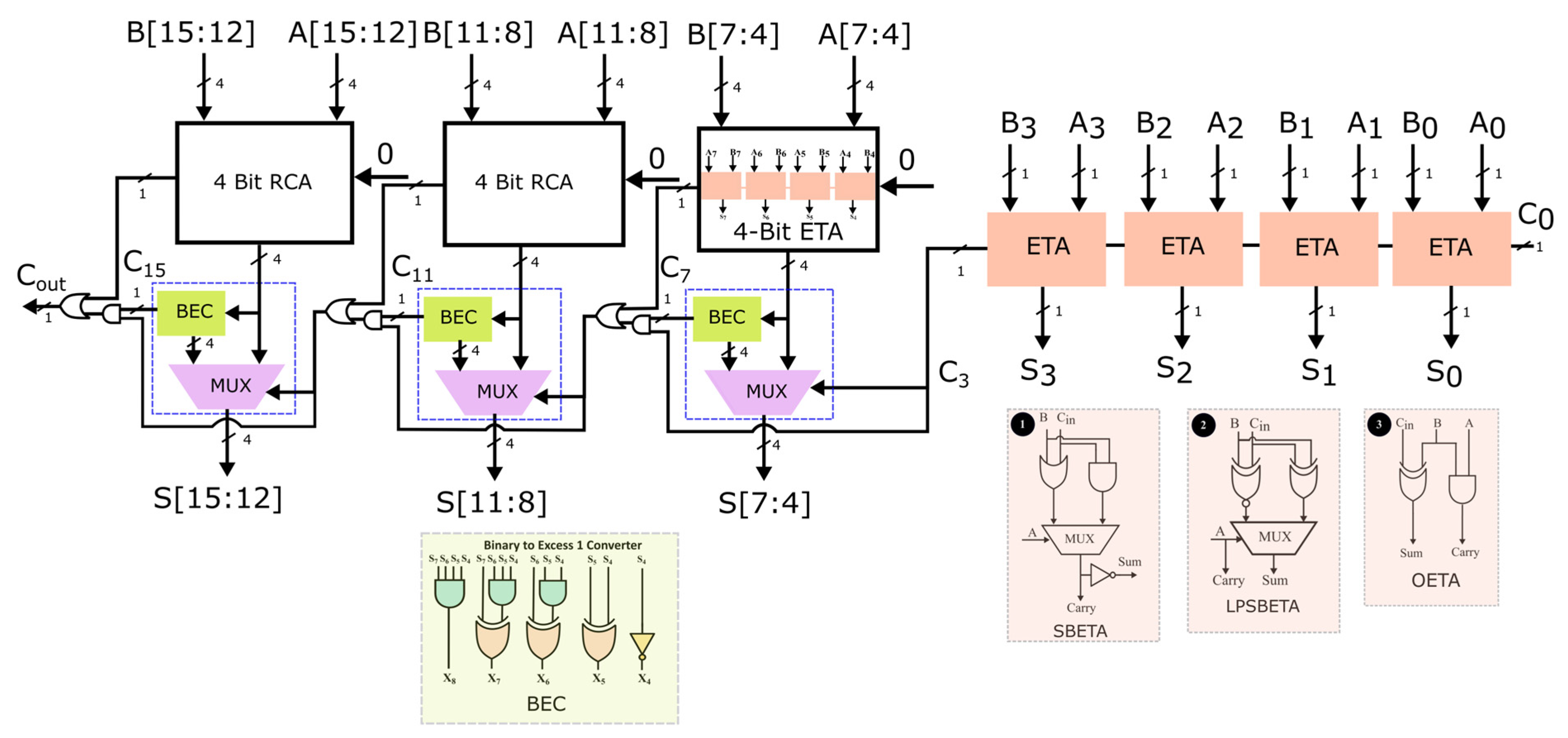
33]. Three designs of ET adders were incorporated in the computational unit as illustrated in
Figure 3, where 1 depicts the logic for the Selector-Based ET Adder (SBETA), 2 describes the logic for Low-Power Selector-Based ET Adder (LPSBETA), and 3 depicts the logic for the Optimized ET Adder (OETA). The pseudocode for SBETA is also depicted.
| Pseudocode: Selector-Based ET Adder |
if (A == 1)
Carry Output = B AND Cin
else
Carry Output = B OR Cin
end |
| Sum Output = NOT (cout) |
While using the approximate computing paradigm, we noted that errors are introduced in the sum and carry output of the ET adders to minimize the complexity of the Boolean expressions, thereby reducing the power and area. The conventional CSLA is modified by incorporating the ET adders for the lower order bits, as illustrated in
Figure 3. The RCA is used for addition when the previous carry is zero. A selector unit is utilized for the higher order bits to reduce the switching activity whenever the previous carry is 1. The power is reduced further by the BEC, that is utilized whenever the carry generated is one.
3.2. Multiplier Based on Divide and Conquer Approach
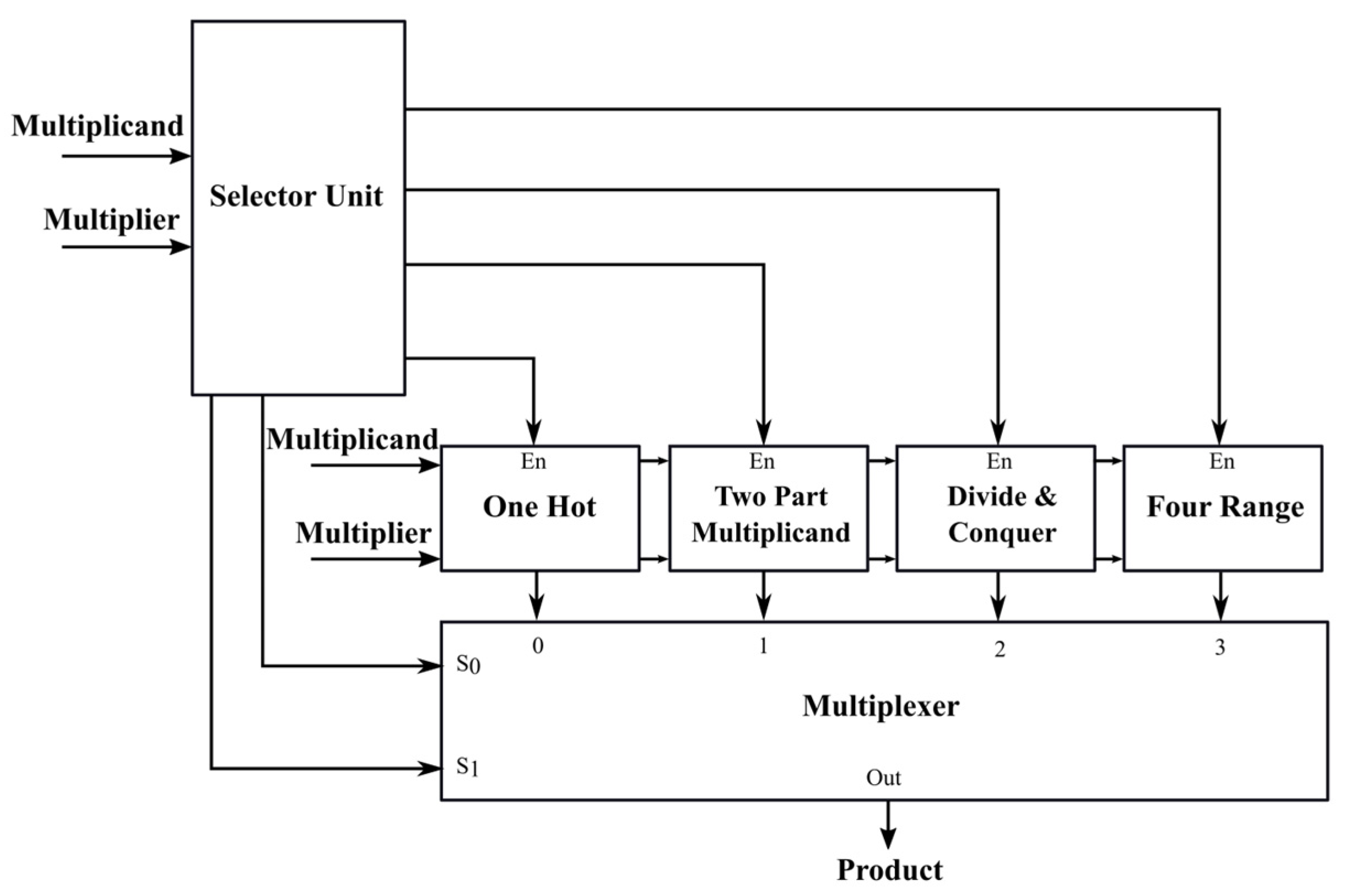
The proposed multiplier based on the divide and conquer approach is illustrated in
Figure 4 and Algorithm 1 depicts the algorithm used. Phase 1 determines the type of multiplier operation to be performed depending on the input type.
| Algorithm 1: Multiplier based on Divide and Conquer Approach |
One Hot Block:
Checks if multiplier/multiplicand is one hot (Input has exactly one bit set to 1).
Two-part Multiplicand Block:
Checks if the multiplier is 3 or less than 99.
Divide and Conquer Block:
Checks if multiplier/multiplicand is an even number.
Four Range Block:
This block is enabled when the conditions mentioned above are not met. |
| In the second phase, just one block is activated, reducing power. |
The detailed algorithm and block diagram is explained here.
- i.
One Hot Block:
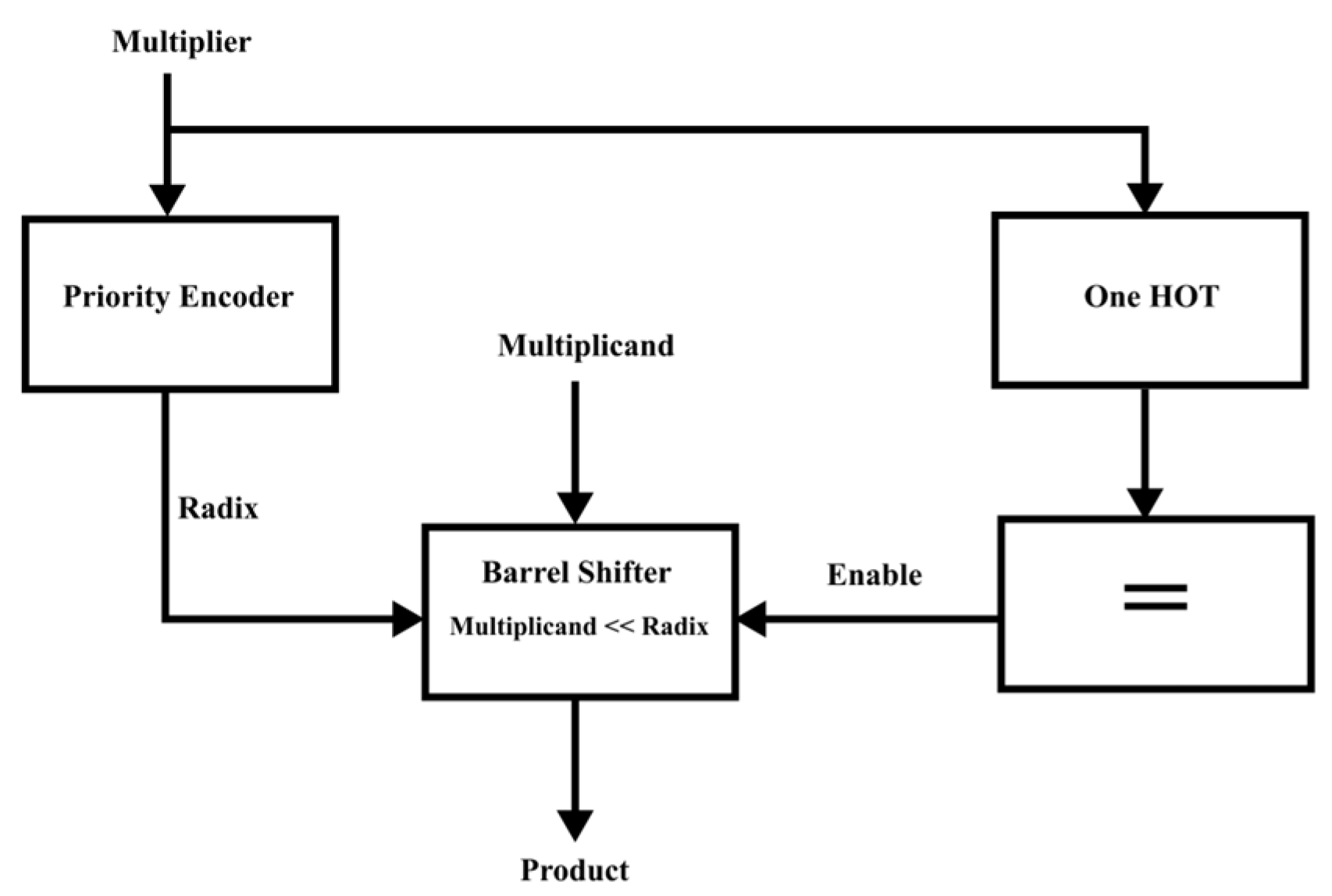
Figure 5 illustrates the block diagram of one hot block. The “Selector unit” determines whether the multiplier/multiplicand is one hot or not.
A one hot flag checks if the multiplier/multiplicand is one hot. A priority encoder determines the radix of the multiplier and multiplicand. The smaller number is made the multiplier based on the radix obtained. The product is obtained by left shifting the multiplicand by the radix of the multiplier when the multiplier is one hot. Likewise, when the multiplicand is one hot, the product is obtained by left shifting the multiplier by the radix of the multiplicand. The shifting operation can be accomplished using a barrel shifter.
- ii.
Two-part Multiplicand Block:
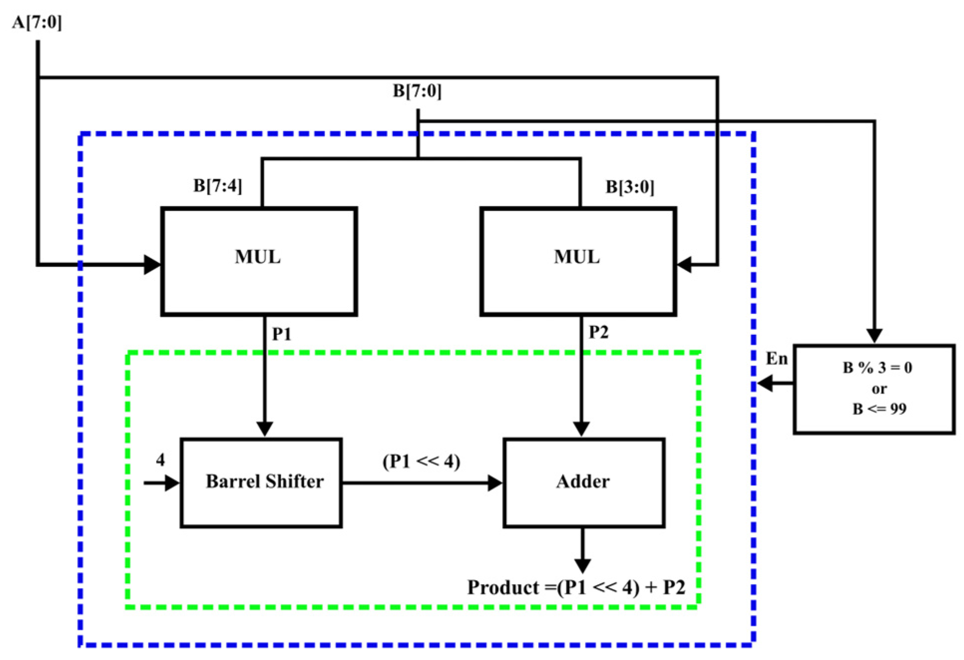
The block diagram of the two-part multiplicand block is depicted in
Figure 6. The “Type Determinant” block determines whether the multiplier is a multiple of 3 or if the multiplier is less than 99. The two-part multiplicand block is enabled if the multiplier represented by B is in the range specified or is a multiple of 3. First, the multiplier is divided into two parts of 4 bits each—B[7:4] and B[3:0]. Each part is multiplied with the multiplier using the MUL block to obtain M1 and M2. A barrel shifter is utilized to left shift M1 by four-bit positions. Finally, the adder block adds the shifted P1 with P2 to obtain the product.
- iii.
Divide and Conquer Block:
The priority encoder block in the proposed architecture determines the range of the multiplicand and multiplier to identify their radix. The numbers to be multiplied represented by A and B are examined to identify if they are even or odd. The even number is designated as the multiplier, and the trailing zeros count is determined. The multiplicand is shifted to the left by the trailing zeros count of the multiplier. The multiplier is shifted to the right by the trailing zeros count of the multiplier. Multiplication is now performed on multiplier and multiplicand to obtain the product. The shifting operation reduces the multiplier range, reducing the power consumption.
Figure 7 shows the block diagram of the divide and conquer block.
- iv.
4-Number Range Block:
The block diagram for the 4-power range method is illustrated in
Figure 8. The radix of the multiplier and multiplicand are determined using a priority encoder. A comparator module then compares the radix of the two numbers to decide which is the smaller number, which is assigned as the multiplier.
The multiplier’s range [L, H] is then decided based on the radix of the multiplier obtained from the priority encoder. The range of the L value is 2n, and 2n + 4 is the H value range. The H and L value average in the range gives the midpoint value (M). A priority encoder is used to determine the radix of H and L. A comparator is used to check if the multiplier is greater than the midpoint value M. If the multiplier is greater than M, the multiplicand is shifted to the left by the radix of H, and the multiplier is shifted to the right by the radix of H. A multiplier calculates the product, which is then added to the multiplicand using an adder. If the multiplier is smaller than the midpoint value, the multiplicand is shifted to the left by the radix of L, and the multiplier is shifted to the right by the radix of L. The product is obtained by multiplying the multiplicand and the multiplier.
3.3. PDP Optimized Multiplier Using Iterative Carry Save SBETA
The demand for image and signal processing systems in portable electronic devices has been on the rise owing to the growing innovations in the field of semiconductor technology. An indispensable component of almost all image processing applications is multipliers. The low-power implementation of multipliers is tricky as it calls for high performance and speed to keep up with modern electronic devices’ increasing clock frequencies.
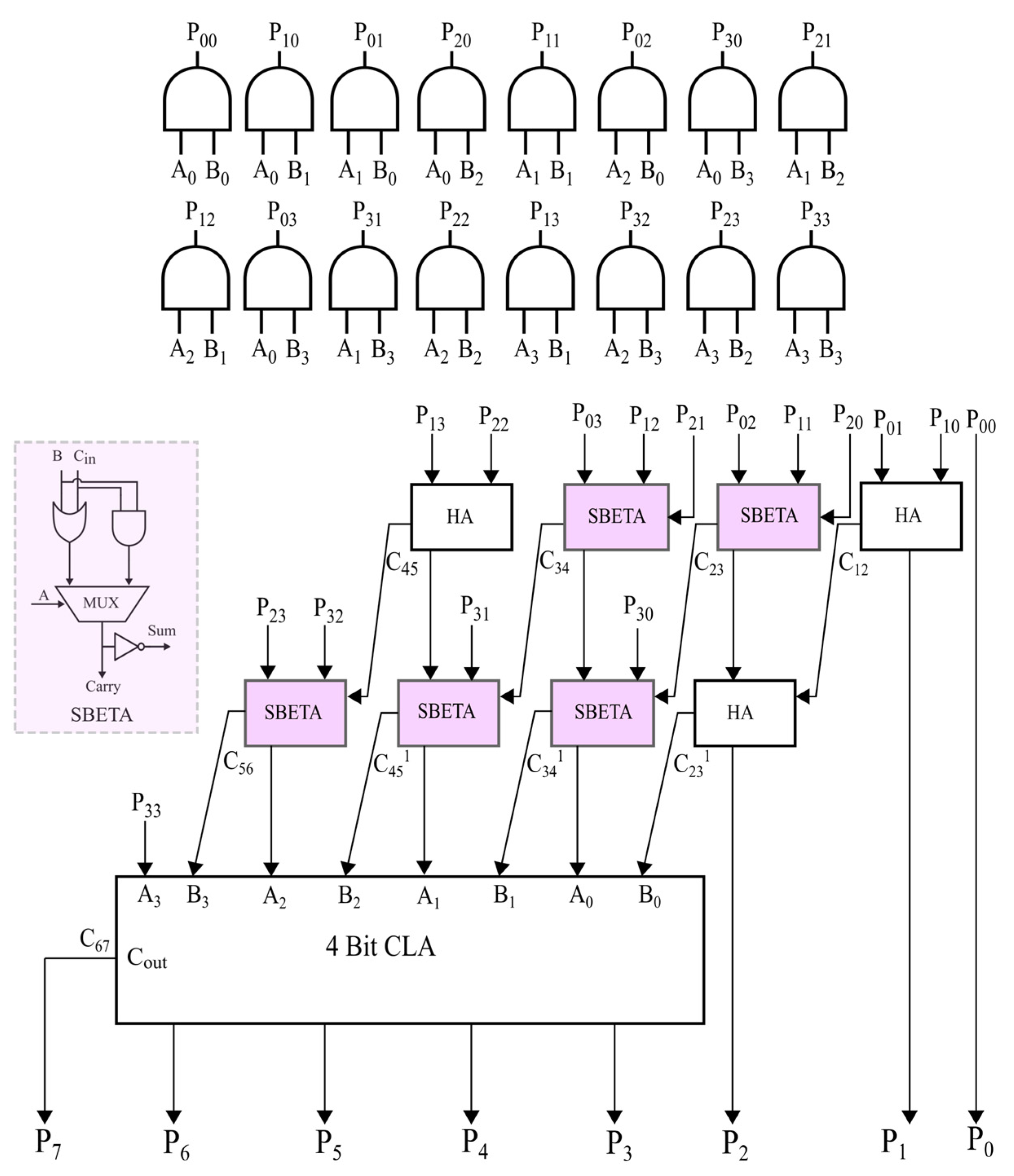
The proposed work discusses about the design and implementation of a multiplier, based on the UT sutra of Vedic arithmetic, incorporating an Iterative Carry Save Selector-Based Error Tolerant Adder (ICS SBETA) for the partial product addition.
In the first phase of multiplication, a 4 × 4 multiplier using ICS SBETA is used as illustrated in
Figure 9. The SBETA design and the partial products generated are also depicted in
Figure 9.
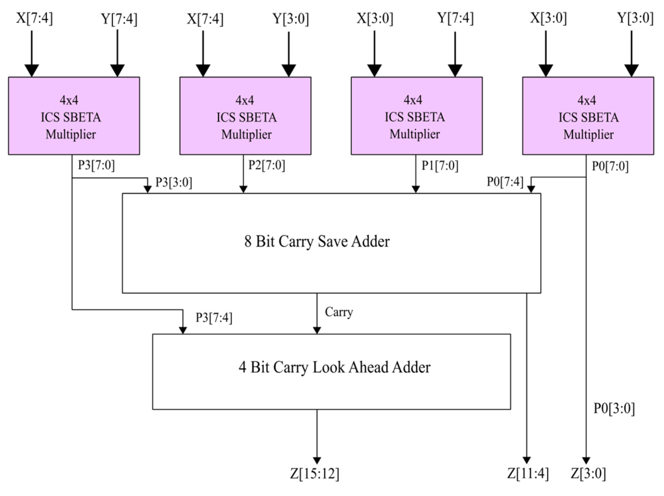
In the second phase, an 8 × 8 multiplier using Iterative Carry Save SBETA is utilized to compute partial products generated in the first stage, as illustrated in
Figure 10.
Finally, in the third phase of multiplication, a 16 × 16 multiplier using ICS SBETA is utilized as depicted in
Figure 11. Since ICS SBETA is incorporated into the multiplier design, the processing time for the summing of partial products is nearly halved. The arithmetic computation using the ICS SBETA is as given by Equation (1).
where
denotes the bit size.
3.4. Logic Unit Using Operand Isolation
The proposed logic module uses the operand isolation technique [
34] to selectively restrict switching activity that propagates through the circuit, hence avoiding unnecessary operations. Operand isolation prevents specific circuit components from detecting changes to their input operands until the desired result is achieved. AND gates, which become transparent when the computation results are required, are used at the circuits’ inputs to achieve this. Operand isolation’s fundamental concept is to power off specific logic blocks while no calculations are being processed. This can be achieved by shutting off the inputs to logic blocks when their outputs are unnecessary. As a result, the unwanted switching activity is minimized, reducing the power.
3.5. Application of the Proposed Computational Unit for Medical Image Compression
This research considers a medical image, a CT scan of the brain for aneurysm detection of size 512 × 512 taken from the open-access database of medical images [
35]. Block style of DCT coding is followed in the DCT approach, in which the DCT is applied over blocks of a fixed size of 8 × 8. So, for an image of size 512 × 512, there are 4096 blocks to which DCT is applied to get the DCT of the entire image. The structure of the encoding of the digital image compression referred to in this research work is depicted in
Figure 12.
The compression ratios can be improvised by replacing the gray code with the binary code when the original digital image is represented and utilized in the image compression process [
36]. A considerable improvement in the compression ratio was observed in this research work by utilizing gray code [
37]. The original image in binary code is first converted to gray code using a binary-to-gray code converter. Gray coding offers a vibrant property of requiring a single bit change from a value “G” to “G + 1” or “G − 1” unlike binary codes, making gray coding an attractive addition to applications demanding lesser power consumption.
Figure 13 illustrates the transitioning of bits for both gray and binary codes from numbers 0 to 15.
The image is then divided into 8 × 8 blocks, to which DCT is applied. Several fast DCT algorithms have been proposed recently for the practical computation of image compression. Most of the proposed algorithms were focused on minimizing the addition and multiplication operations associated with the butterfly blocks incorporated in the DCT algorithms. The algorithm proposed by Loeffler proved to be the fastest, with just 11 multiplications and 29 additions, making it the ideal choice for this research work [
38]. The structure of the 8-point DCT structure incorporating the computational unit in Loeffler’s algorithm is illustrated in
Figure 14. The adders used for computations in the butterfly diagram are replaced by the ET adders by incorporating the computational unit designed in this research work, reducing the power. The multiplications involved are reduced by approximating the cosine constants as given in
Table 3 to one wherever applicable, and in cases where multiplications were required, it was achieved using the low-power multipliers and shifters, as illustrated in
Figure 14.
The bit-width of the digital input images is 10 bits, and after the row DCT, the output images’ bit-width is 14 bits. The second column DCT and first row IDCT had an input and output bit-width of 14 bits. Finally, 14 was the bit-width of the last column IDCT, with the output image having a bit-width of 10 bits.
The next step is quantization, where the high-frequency DCT coefficients that are not imperative are reduced to 0. The quantization process is achieved by dividing each 8 × 8 block by a coefficient Q (u,v) obtained using the quantization matrix. As the division involved is an integer computation, most coefficients are 0, whereas the remaining coefficients are smaller numbers. A situation ideal for run length encoding and entropy encoding is obtained now. The quantization matrix determines the quality of the compression. Larger values in the quantization table are chosen for lower quality, resulting in higher compression rates.
A quality factor of 50 was utilized for the quantization process. Each matrix element should be multiplied by (100 − q)/50 for higher qualities; the multiplication factor is 50/q for lower qualities. The high-frequency components are eliminated without compromising the image quality. Higher numbers are located at the bottom right of the quantization table, whereas data with high-frequency and low-frequency values are located at the top left. This makes the high-frequency components to be rounded off to zero. Once the DCT coefficients are quantized, a zig-zag scanning pattern, as depicted in
Figure 15, is followed to maintain the redundancy of zeroes due to the presence of several zeroes at the bottom left corner. The high-frequency components are reduced to zero once quantization is fulfilled, due to which the zig-zag pattern of scanning is pursued.
The list of integer values obtained after zig-zag scanning generates the sequence of symbols. Run Length Encoding (RLE) is the next step since there are many zeroes from which each number, along with the number of times it is repeated, is obtained. The quantized coefficients are sampled using the zig-zag scan pattern from the lowest to highest frequencies to generate longer runs. The data stream obtained has a length of 64 bytes, which has a high probability of zeros toward the end. The RLE of the stream obtained is highly efficient.
After this, Huffman Coding must be carried out, where the numbers with higher frequency are denoted with lesser bits than the other numbers. RLE and Huffman Coding are performed to reduce the space required without removing any data. The data obtained are then converted back to binary format using the gray-to-binary code converter, after which the compressed image is obtained [
38,
39,
40,
41,
42].
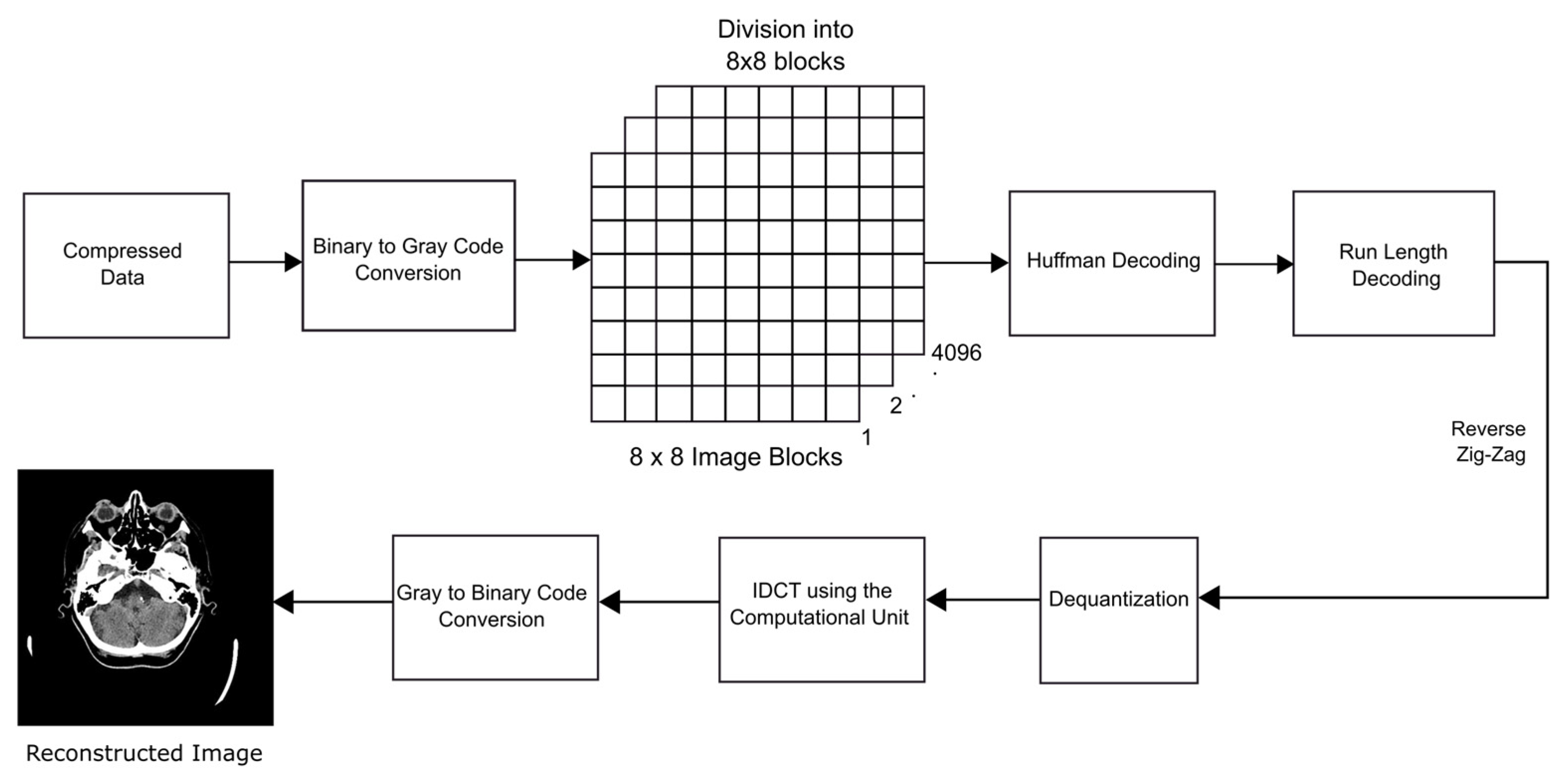
The reverse process is applied to obtain the reconstructed image using the decoding process illustrated in
Figure 16. The Huffman-coded data are decoded, and the run-length encoded data are expanded into an 8 × 8 matrix to restore the matrix of quantized coefficients. These are multiplied by the values from the quantization matrix Q (u,v). Next, the Inverse Discrete Cosine Transform (IDCT), which is the reverse of the DCT, is carried out on the values obtained in a similar manner using the computational unit for the computations involved. At this instant, data loss becomes evident as the DCT coefficients that were set to zero due to rounding remain zero after decompression.
5. Conclusions
The ASIC design of computational units is vital for processors, especially in contemporary technologies. The research work’s prime focus was designing, developing, and implementing an ASIC-based computational unit using the concepts of low-power VLSI, mainly approximate computing, multipliers based on UT sutra utilizing ICS SBETA, operand isolation, and low-power multipliers for stand-alone medical image processing applications. This research covers implementing an ASIC-based computational unit for medical image compression applications. The synthesis was performed with standard semi-custom ASIC design flow using the Genus tool of Cadence. In addition, 45 nm gpdk technology libraries were used to synthesize the image compression architecture designed using the computational unit with Loeffler’s algorithm, resulting in improved performance compared to existing architectures. The PSNR and SSIM of the proposed design were better than the existing architectures due to the incorporation of the computational unit. A significant reduction in PDP and an improved PSNR for VLSI implementations was observed in the synthesis results when carried out on a medical image
The research work can be explored further by including the ET adders in convolution or digital filter applications involving addition. Future work involves replacing the standard libraries with the optimized digital libraries from Taiwan Semiconductor Manufacturing Company Limited (TSMC) and realizing the design up to chip fabrication. The design can be extended further to make it suitable for the high real-time performance required for video compression coding. The incorporation of low-power techniques can be explored to reduce power. Other multiplier and adder designs can be analyzed to form different combinations of computational units suitable for image processing applications. Different signal processing algorithms can also be explored and implemented using the proposed computational unit.
The developed computational unit for image compression that was utilized in the DCT algorithm demonstrates significant potential for direct application in medical image compression. The DCT-based computational unit can substantially reduce the storage requirements, enabling healthcare providers to maintain comprehensive image archives without the necessity of extensive physical storage infrastructure. The hospitals can save on storage costs and enhance data management practices, facilitating quicker retrieval and review of patient images by efficiently compressing images. Compressing medical images reduces their file size, which can be advantageous for encryption processes. Smaller file sizes can be encrypted more quickly and with potentially less computational overhead, thus enhancing the overall security of medical image data. Ensuring the confidentiality and integrity of medical images is critical, and the DCT-based computational unit can play a vital role in facilitating secure storage and transmission protocols.
The computational unit can be used to efficiently handle medical images on mobile platforms, allowing healthcare providers to review and share images using smartphones and tablets. This flexibility supports a wide range of healthcare scenarios, from emergency response to routine check-ups, enhancing the accessibility and responsiveness of medical services. In wearable medical devices, DCT compression can compress and transmit data, reducing power consumption and increasing device lifespan.
The implementation of this computational unit not only addresses current challenges but also paves the way for future advancements in medical image processing. Continued development and optimization could lead to even more efficient compression algorithms, further enhancing the utility and applicability of this technology in diverse medical environments. Additionally, integrating machine learning techniques could refine the compression process, ensuring that diagnostically relevant features are preserved with even greater precision.
The DCT-based computational unit designed for image compression presents an effective tool for medical image compression, with direct applications that can significantly enhance storage, transmission, and overall management of medical images. Its integration into healthcare systems promises to improve operational efficiencies, reduce costs, and ultimately contribute to better patient care outcomes.

