Article

Quad-Band Rectifier Circuit Design for IoT Applications

by
Ioannis D. Bougas
1,*,
Maria S. Papadopoulou
1,2,
Achilles D. Boursianis
1,
Sotirios Sotiroudis
1,
Zaharias D. Zaharis
3 and
Sotirios K. Goudos
1,*
1
ELEDIA Research Center, ELEDIA@AUTH, School of Physics, Aristotle University of Thessaloniki, 54124 Thessaloniki, Greece
2
Department of Information and Electronic Engineering, International Hellenic University, Alexander Campus, 57400 Sindos, Greece
3
ELEDIA@AUTH, School of Electrical & Computer Engineering, Aristotle University of Thessaloniki, 54124 Thessaloniki, Greece
*
Authors to whom correspondence should be addressed.
Technologies 2024, 12(10), 188; https://doi.org/10.3390/technologies12100188
Submission received: 2 August 2024 / Revised: 30 August 2024 / Accepted: 12 September 2024 / Published: 2 October 2024
(This article belongs to the Special Issue IoT-Enabling Technologies and Applications)

Abstract

:
In this work, a novel quad-band rectifier circuit is introduced for RF energy harvesting and Internet of Things (IoT) applications. The proposed rectifier operates in the Wi-Fi frequency band and can supply low-power sensors and systems used in IoT services. The circuit operates at 2.4 , 3.5 , 5, and 5.8 GHz. The proposed RF-to-DC rectifier is designed based on Delon theory and Greinacher topology on an RT/Duroid 5880 substrate. The results show that our proposed circuit can harvest RF energy from the environment, providing maximum power conversion efficiency (PCE) greater than 81% when the output load is 0.511 kΩ and the input power is 12 dBm. In this work, we provide a comprehensive design framework for an affordable RF-to-DC rectifier. Our circuit performs better than similar designs in the literature. This rectifier could be integrated into an IoT node to harvest RF energy, thereby proving a green energy source. The IoT node can operate at various frequencies.

1. Introduction

The Internet of Things (IoT) can make the world more green, efficient, and connected. The need for a wireless and autonomous battery management system has become more urgent due to the number of devices used per household. The answer to this situation is power harvesting that allows a circuit to operate on its own energy from the environment.
Physical devices in an IoT network are connected through numerous wireless networks and systems. The different nodes and devices connected to IoT systems are noticeably high. It is estimated that there will be more than 30 billion IoT-connected devices by 2025, accounting for almost four per person on average. Thus, this imposes an impressive challenge to self-sustainability [1].
The electromagnetic energy that exists in the environment can resolve energy issues in next-generation systems. Radio frequency energy harvesting (RFEH) could be a viable solution to meet the energy demands of wireless systems, such as portable devices that need to be recharged several times a day. Research on wireless power transmission (WPT) and RF energy harvesting in the millimeter and microwave ranges has been a dynamic area of research in recent years [2]. This technique can power many devices wirelessly and can also prove useful for diagnostic and therapeutic implantable devices [3], robotics [4], wireless sensor networks, wireless charging, and military devices [5].
The use of batteries is challenging for many economic, environmental, and practical reasons. Alternative energy sources can complement or even replace batteries [6]. Several methods for scavenging energy have been proposed. Nevertheless, a system without batteries for energy harvesting to convert RF to DC power is much preferred. This approach provides a consistent, clean, and green energy solution for portable low-power systems.
The WPT is divided into two main categories: far-field microwave power transmission and near-field magnetic inductive powering [7,8]. Far-field microwave power transmission provides power delivery at a long distance, while near-field power transmission is restricted by a short transmission distance. With the growth in communication technology, it is possible to scavenge the radio frequency (RF) signals of the environment through microwave power transmission. Various types of transmitters, such as radio towers, mobile phones, televisions, Wi-Fi routers, and base stations, can continuously charge numerous low-power devices [9].
A rectenna system (rectifying antenna) is composed of an antenna, a rectifier circuit, an IMN (impedance matching network), and a DC–DC converter [10,11]. The antenna collects the electromagnetic waves from the environment and drives them to the rectifier circuit. The rectifier converts ambient RF signals to DC power. The DC–DC converter boosts the rectifier’s output. The IMN has to provide the desired impedance matching between the receiving antenna and the rectifier with minimal energy losses. Figure 1 shows a typical RF energy harvesting system.
There are several frequency bands in the environment that are distributed over a wide range. Hence, many rectennas work in different frequency bands. The RF range is part of the electromagnetic range that begins from VHF (very high frequencies) to EHF (extremely high frequencies), ranging from 3 kHz to 300 GHz. Prominent transmission systems including FM radio (87.5–108 MHz), VHF and UHF DTV, GSM-900, GSM-1800, UMTS-3G, LTE-4G, Wi-Fi, Bluetooth, GHz, and 5G utilize the RF range for broadcasting and communication purposes [12].
In RFEH, the main challenge faced is the low RF power density available in the environment. To evaluate the possible locations of RF energy harvesters, the level of RF power must be measured in the sensor environment. Hence, due to the multitude of sensor applications, these measurements must take place in various environments, such as cities, villages, and the countryside [13,14]. The solution to this problem is the design of broadband or multi-band rectenna systems to collect RF energy from different frequency bands to increase power conversion efficiency (PCE) [15].
The rectifier is the key part of the rectenna system that affects the efficiency of the whole system [16]. The design of the rectifiers has to be very compact. Rectifiers can transfer energy with minimal losses to other parts of the rectenna. In IoT networks, there is a huge number of applications for rectifiers. For example, in [17,18,19,20,21], there are applications in which a rectifier is vitally important. Usually, rectenna systems are manufactured to operate at frequencies that are important for wireless communications and broadcast services.
In this work, we designed a quad-band rectifier that works in the Wi-Fi band [22] and, more specifically, at 2.4 , 3.5 , 5, and 5.8 GHz. The RF power density of a GSM base station is higher than the signal from a Wi-Fi router. The distance of a Wi-Fi router is very small (indoor environments); thus, higher power levels can be harvested [23].
The remainder of this work is organized as follows. Firstly, we present the materials and methods in Section 2. In Section 3, we present the design framework. In Section 4, we present the complete design of the proposed quad-band rectifier and the numerical results. In Section 5, we discuss the contributions of this work and its main results. Finally, Section 6 summarizes the concluding remarks of our work.

2. Materials and Methods

2.1. Related Work

Rectifiers, which are responsible for transforming RF signals into DC power, can be broadly classified into integrated designs such as CMOS and monolithic microwave integrated circuits (MMICs), as well as discrete designs utilizing diodes or transistors. Numerous noteworthy studies in the bibliography investigate these design techniques [24,25,26,27,28,29,30].
In [1], the authors designed a multiband rectenna for RF energy harvesting. The proposed rectifier circuit achieves 78% PCE. The authors in [9] manufactured a rectenna system that achieves a maximum power conversion efficiency of 60% at 2.45 GHz and 53% at 3.5 GHz, for input power 0 dBm. In [15], we can find a dual-band rectifier circuit design that achieves 53% power conversion efficiency at 3.5 and 5 GHz, for input power 12 dBm. The circuit was designed on a Rogers RT/Duroid 5880 substrate. The authors of [31] designed a rectifier circuit with a PCE of 51.3 %, a frequency of 5.1 GHz, and an output load of 350 Ω . In [32], the designers manufactured a bridge rectifier that operates at 5 GHz. The circuit’s PCE is up to 36.4 %.
In [33], the authors manufactured a full-wave (FW) rectifier that operates at sub-6 GHz in 5G bands with a central frequency of 3.5 GHz. This rectifier achieves a maximum power conversion efficiency equal to 42.5 % when the output load is 1.1 kΩ and the input power reaches 9 dBm. The authors in [34] designed, at a frequency of 3.5 GHz, a Villard voltage doubler that reaches 42% PCE with 14 dBm input power. In [35], the authors presented a full-wave rectifier that achieved 39.6 % power conversion efficiency at 3.8 GHz using an HSMS-2820 Schottky diode. In [36], the authors designed a rectenna that can scavenge energy from WiMAX and Wi-Fi bands. This half-wave circuit (HW) is on a Rogers RT/Duroid 5880 substrate and operates at 3.5 GHz with a 0 dBm input with an efficiency of 44%. A full-wave rectifier was manufactured in [37] with a PCE of 29.7 % for an input power of 6 dBm at 3.5 GHz.
An HW rectifier can be found in [38]. This circuit using the SMS-7630 diode achieves a PCE of 42.5 %, for input power equal to 10 dBm. In [39], we can find a rectenna system that works at 2.4 , 4, and 5 GHz. The authors in [40] designed a triple-band rectenna that achieves 53%, 31%, and 15.56 % power conversion efficiency at 2, 2.5 , and 3 GHz, respectively. The authors in [41] designed a full-wave rectifier on a Rogers RO3003 substrate with 0 dBm as input power and two Schottky diodes, SMS7630-079LF. They reached a power conversion efficiency of 42% at 3.5 GHz. In [42], the authors, using SMS7630 diodes, manufactured a rectifier that works with GSM900, GSM1800, UMTS2100, WiMax 3500, and Wi-Fi ( 2.4 and 5 GHz). They achieved 33.5 % maximum PCE at 15 dBm when the frequency was 1.8 GHz.
A dual-band rectifier was manufactured in [43], which achieves 49.9 % PCE with 1.1 kΩ load resistance and 0 dBm input power at 5 GHz. The authors in [44] fabricated a rectenna circuit for the frequency range of 1.8 , 2.4 , 5.8 , and 3.8 GHz. They achieved PCE equal to 62.69 % for input power 0 dBm. The rectenna proposed in [45] achieves maximum PCE equal to 69.3 % at 2.4 GHz. In [46], we can find a rectifier circuit design that works at 2.45 GHz. They achieve maximum PCE 57% for input power 5 dBm. The authors in [47] designed a bridge rectifier. The maximum power efficiency is equal to 80% at 10 dBm input power.
In [48], we can find a rectifier circuit that was designed to operate at the 5.8 GHz Wi-Fi frequency band using SMS7630-061 Schottky diodes. In [49], we can find a half-wave rectifier that achieved 63.5 % efficiency for 0 dBm input power. The authors in [50] presented a rectifier circuit that operates at 5.8 GHz using HSMS-286B diodes. In [51], the authors fabricated a full-wave rectifier, which achieves 60% power conversion efficiency. In [52], the authors manufactured a high efficiency RF–DC converter and achieved a high output voltage of 34.2 V.

2.2. Design Methodology

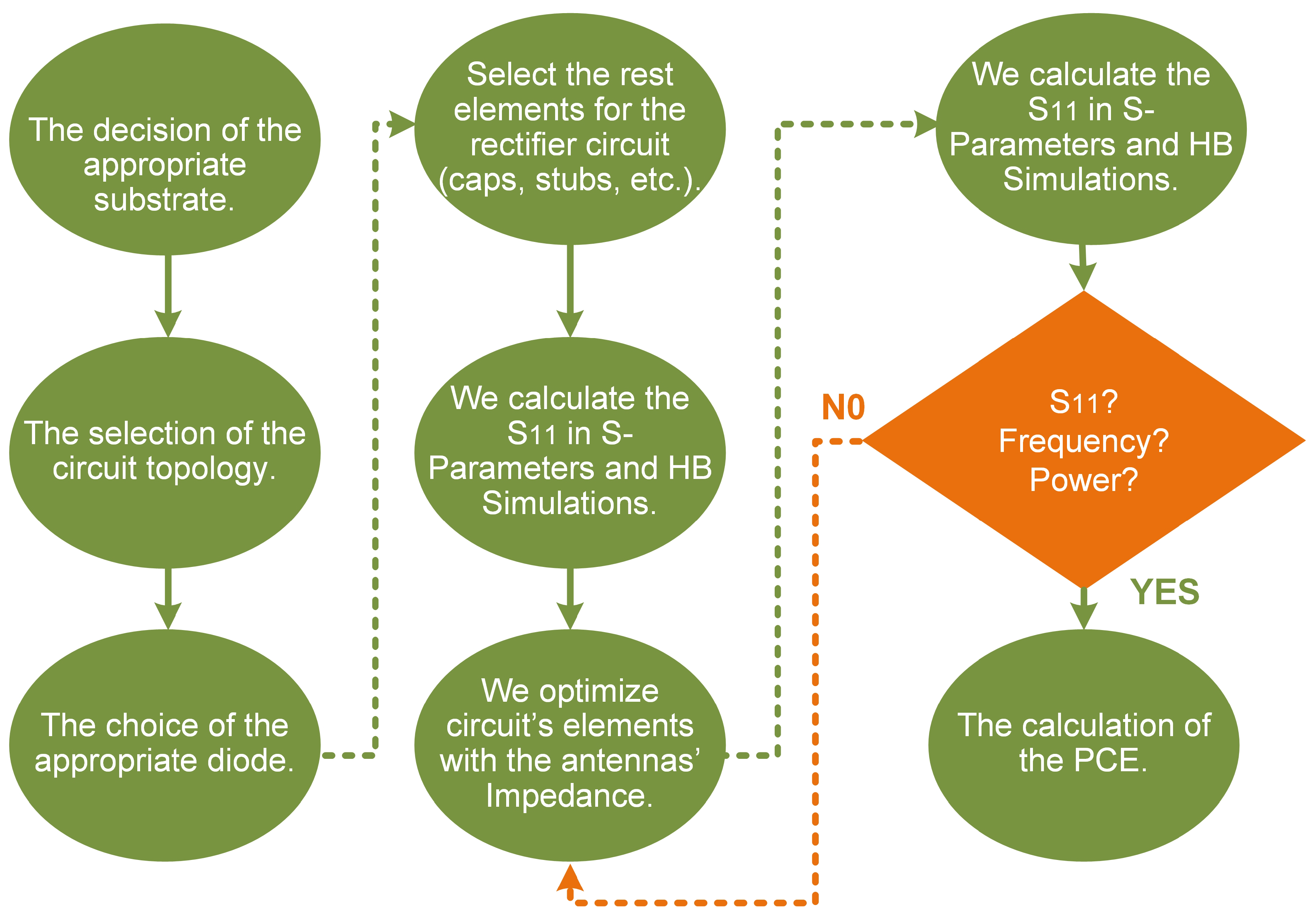
In this work, we present a quad-band rectifier circuit that operates in the whole Wi-Fi range at frequencies 2.4 , 3.5 , 5, and 5.8 GHz. The rectifier circuit design procedure consists of four main steps: defining the proper substrate, choosing the circuit topology, selecting the appropriate diode, and designing an efficient IMN [10]. The design of each part must be well-developed to ensure that the whole system develops in a feasible way [16].
The decision regarding the appropriate substrate is a key part of the design procedure. The ideal substrate for a rectifier circuit would be a substrate with a low dielectric constant and low dielectric loss. The selection of the circuit topology is the main thing to consider before selecting the individual elements of the circuit. The choice of the appropriate diode is another very important step in the procedure, since we want a diode that gives us a high conversion efficiency because of its characteristics. After that, we must select the rest of the elements for the rectifier circuit (caps, stubs, etc.). The next step is to calculate the frequency response ( S 11 ). We adjust the circuit elements with the antenna impedance (impedance matching network) and recalculate the S 11 . If we reach the desired values for frequency, S 11 , and power, then we calculate the PCE of the overall system. Otherwise, we return to the previous calculations [15]. Figure 2 displays the methodology.

2.3. Contribution

The main contribution of this work lies in the following:
  • We introduce a novel quad-band rectifier circuit that operates in the whole Wi-Fi range.
  • We discuss and provide a complete design framework for a low-cost RF-to-DC rectifier.
  • We propose a novel IMN (impedance matching network) that comprises two discrete branches, one for 2.4 and 3.5 GHz, and the other for 5 and 5.8 GHz. Each branch consists of a combination L and reverse L-shaped network with rectangular and radial stubs.
  • We design a rectifier circuit that operates at 2.4 , 3.5 , 5, and 5.8 GHz simultaneously.
  • Our rectifier design performs better than similar designs in the literature.
  • This rectifier could be part of an IoT node to harvest environmental RF energy, therefore providing a green energy source. The IoT node can operate at different frequencies.

3. Design Framework

3.1. Receiving Antenna

The key role of the receiving antenna in a rectenna system is to collect as many RF signals as possible. The reflected power at the antenna input, the efficiency of the antenna, the impedance, the gain, and its weight and size are the basic factors that are considered in the design of an antenna. Among the most common antenna types are the log-periodic dipole arrays [53], the monopole antennas [54], the dipole antennas [55], the fractal antennas [56], the Yagi–Uda antennas [57] the bowtie antennas [58], the loop antennas [59], the dielectric resonator antennas (DRAs) [60], and the planar inverted F antennas [61]. Furthermore, the microstrip antenna [62] is one of the common designs found in the literature for RF energy harvesting.

3.2. Topology of the Rectifier

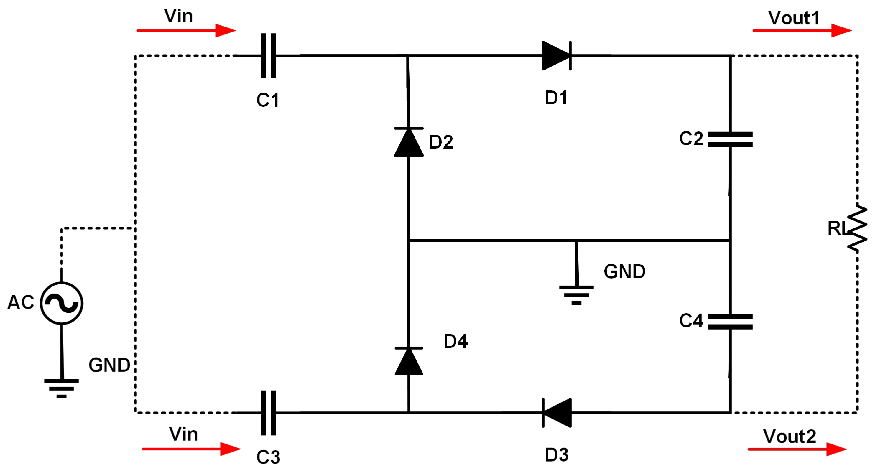
The design theory of a rectifier circuit looks mature. Circuit designers often need mathematical simulators to design RF rectifier circuits. They must search for many topologies and find the best load resistance or input matching impedance. RF rectifiers are expected to maximize the RF energy they receive as much as possible. This requirement is very important for energy harvesting and wireless power transfer applications [63]. The main topologies for a rectifier design are the diode bridge, the single diode, and the voltage multiplier. We selected a Greinacher voltage multiplier for our circuit because this topology converts and amplifies the AC input to the DC output [5,64]. The circuit consists of two diodes (D1, D2) and two capacitors (C1, C2). In this circuit, a half-wave of input sinusoidal voltage surges through one diode. Then, the opposite half-wave passes through the other. Repeating the process amplifies the voltage to double and charges the final capacitor. Hence, in the output, there is double voltage [65]. Figure 3 displays the Greinacher voltage multiplier.
We classify the ground as GND, the AC input source as AC, the output load as R L , and the input and output voltage as V i n and V o u t , respectively.
Our rectifier is based on the Delon voltage doubler topology. Jules Delon, a French engineer, presented his topology in 1908 in Marseilles. The idea is to combine two HW rectifier circuits on top of each other. The load in this circuit is related to the differential path. The voltage in the output load is the difference between the two outputs [66]. Our rectifier has two branches, and each branch consists of a Greinacher topology. Figure 4 shows our selection for the rectifier topology.

3.3. Substrate

The choice of the substrate is a key part of the design procedure for rectifier circuits. The low dielectric loss and the low dielectric constant are the most important characteristics. Hence, for our design, we select the substrate RT/Duroid 5880. It has a dielectric loss tangent of 0.0009 , a thickness of 0.508 mm, a copper thickness of 0.035 mm, and a dielectric constant of 2.2 [67]. These characteristics mean that this substrate is appropriate for high-frequency applications, such as the proposed quad-band rectifier that works at 2.4 , 3.5 , 5, and 5.8 GHz. Figure 5 shows what the substrate looks like.

3.4. Diode

Diodes are a key component in rectifier circuit design. Usually, in the environment, there are only low power levels. The magnitude of the incident signal can be equal to the V T H (voltage threshold) of the diode. So, the diode losses become predominant [68].
The conversion efficiency of the rectifier is related to the diodes. Equations (1) and (2) below give us the PCE of the circuit:
P m = i = 1 n P f i ,
n m = P m P L O S S P m ,
where P L O S S , n m , P m , n, P f i , are the power loss related to the diode, the power conversion efficiency of the rectifier, the input power of the rectifier circuit, the number of operating bands, and the power of each operating band, respectively [1].
In rectifier circuit designs, the most commonly used are Schottky diodes because they have fast switching capabilities and detect very low signals [69,70]. For this voltage multiplier, we selected the HSMS-286C Schottky diodes [71]. These diodes have been manufactured and optimized to operate at frequencies between 915 MHz and 5.8 GHz. According to the manufacturer, these diodes are ideal for detector circuits and voltage doublers [72]. We achieved a high conversion efficiency because of their features.
We can see these features below:
  • Barrier capacitance C J 0 = 0.18 pF ;
  • Series resistance R S = 6 Ω ;
  • Breakdown voltage B V = 7 V ;
  • Typical capacitance C T = 0.25 pF ;
  • Forward Voltage V F = 250 350 mV .

3.5. Impedance Matching Network

In the literature, there are numerous types of impedance matching networks. These networks consist of distributed elements such as microstrip lines and stubs or lumped elements such as inductors and capacitors. The design of these networks is the main difference among the plethora of rectifier designs in the literature. These networks ensure that there will be power transfer with minimal losses from the receiving antenna to the rectifier circuit. In addition, this prevents any irrelevant RF energy from reaching the rectifier from the receiving antenna, affecting the efficiency of the rectifier in the main band of interest [73,74]. This network guarantees a minimum power reflection of the signal back to the source [75].
The proposed rectifier operates at 2.4 , 3.5 , 5, and 5.8 GHz; hence, we chose distributed elements because they are appropriate at frequencies between 3 and 300 GHz. At frequencies below 3 GHz, the lumped elements are generally used [10].
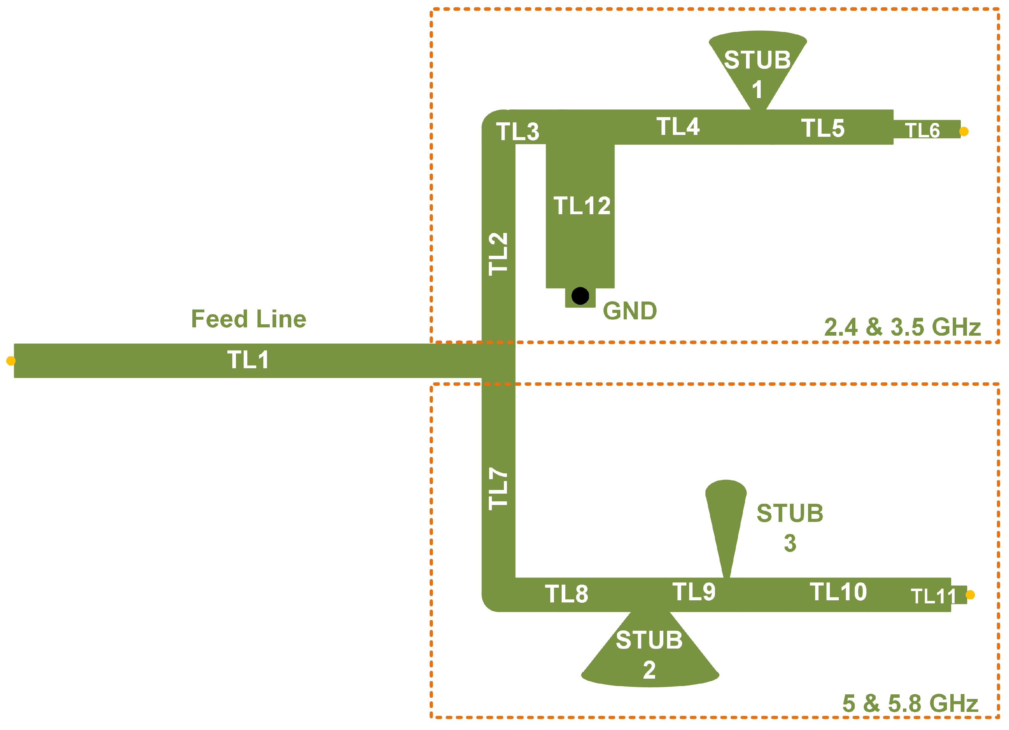
The proposed impedance matching network consists of two different branches: one for 2.4 and 3.5 GHz and the other for 5 and 5.8 GHz. Each branch consists of a combination of L and reverse L-shaped networks with rectangular and radial stubs. In addition to regular stubs, we select radial stubs because they require less space on the chip. Moreover, regular stubs are better at lower frequencies, such as at 2.4 GHz [1,76]. Figure 6 illustrates the proposed IMN circuit. In Table 1, we can find the physical parameters of the transmission lines and stubs of our impedance matching network.

3.6. DC–DC Converter

A high-gain DC–DC converter is applied as an interface circuit between the rectifier and the load to boost and stabilize the output of the rectifier [15]. This type of DC–DC converter has to achieve a high voltage conversion ratio and should have small dimensions. The growth of high-voltage gain converters has emerged as one of the most important additions in the design of renewable energy systems, and more specifically in RF energy harvesting systems where the power level is too low. In the literature, numerous DC–DC converters can achieve high-voltage conversion ratios. Renewable energy applications and IoT systems generally use isolated or non-isolated classes of high step-up DC–DC structures [77,78].

4. Numerical Results

4.1. Proposed RF-to-DC Rectifier Circuit Results

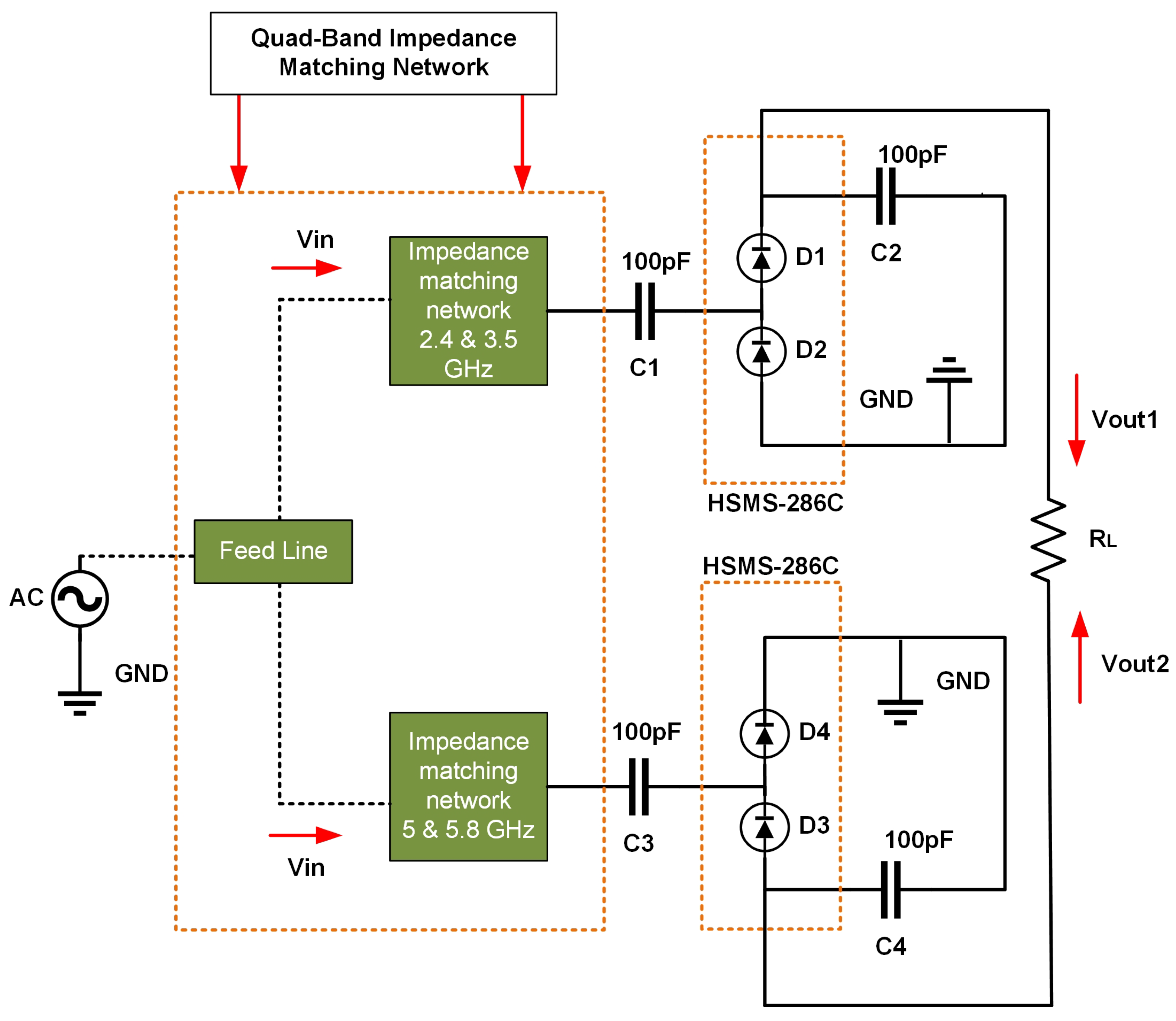
We introduce the novel design of a quad-band rectifier circuit design on the RT/Duroid 5880 substrate. The presented impedance matching network is a network with two distinct branches: one for 2.4 and 3.5 GHz and one for 5 and 5.8 GHz. As mentioned in Section 3, each branch consists of a combination of L and reverse L-shaped networks with rectangular and radial stubs. We designed and then connected two full-wave Greinacher voltage multipliers, one for each branch, based on the Delon theory.
The voltage doublers were built with HSMS-286C Schottky diodes and two sc-avx-ACCU-F-08053K-F-19960828 with 100 pF capacitors. In addition, the circuit encloses several conductor lines of suitable width (W) and length (L) to connect all components (capacitors, diodes). The output load is connected differentially. Consequently, we created a differential rectifier circuit design to achieve higher output voltage and power at low input power [79]. We used the gradient optimizer algorithm from the commercial software Advanced Design System (ADS) from Keysight Technologies to design and optimize this rectifier circuit. Figure 7 displays the complete circuit design of the proposed quad-band rectifier. The quad-band impedance matching network (IMN) described in the previous section is used here. The input signal is received by an antenna connected to the feed line via an SMA (SubMiniature version A) connector. Each branch of the network is designed to operate at two different frequencies. The input signals choose the optimal path, either through one branch or through both, depending on their frequency.
As input for designing the rectifier circuit, we used an antenna port of Z A = 50 Ω , while as an output load, our option is a resistance of 511 Ω. The initial impedance of the rectifier circuit is 18.70 − j1.66 at 2.4 GHz, 3.19 − j 27.00 at 3.5 GHz, 52.46 + j14.45 at 5 GHz, and 15.53 + j28.46 at 5.8 GHz. The goal of the proposed impedance matching network is to match the rectifier circuit to the impedance of the antenna (antenna port). We calculated the impedance of the rectifier to be 52.62 − j0.16 at 2.4 GHz, 49.31 − j4.28 at 3.49 GHz, 47.84 − j1.25 at 4.99 GHz, and 50.04 + j0.86 at 5.8 GHz. Figure 8 depicts the frequency response of the reflection coefficient ( S 11 ). The S 11 value at 2.4 , 3.49 , 4.99 , and 5.8 GHz is 31.85 , 27.22 , 31.86 , and 41.34 dB, respectively. In addition to that, the same figure displays the bandwidth (BW) ( S 11 < 10 ). This quad-band rectifier is equal to 20 MHz at 2.4 GHz, 60 MHz at 3.49 GHz, 80 MHz at 4.99 GHz, and 59 MHz at 5.8 GHz.
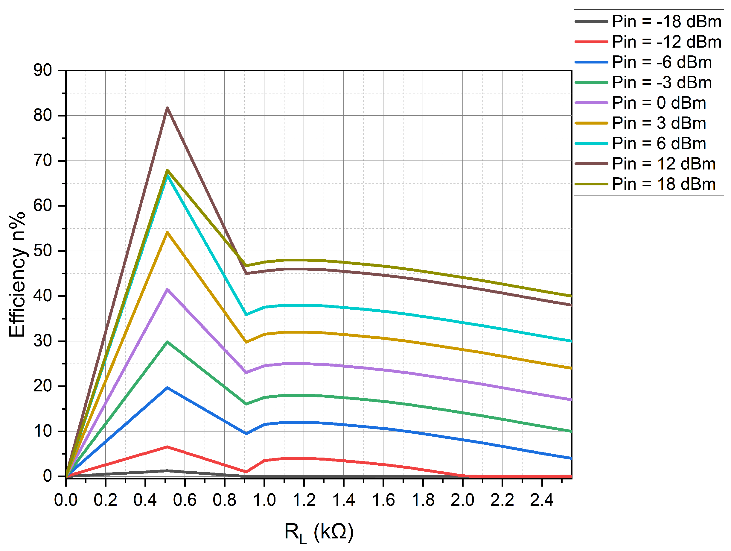
The selection of the output load is one of the most critical parts of the design process because it determines the total RF-to-DC efficiency n% of the rectifier circuit. Equations (3) and (4) express the power efficiency n%, and we can see that it decreases when the output load increases. The impedance of the energy harvesting circuit is dependent on a variety of factors, including input power level, operating frequency, load impedance, and rectifier or voltage multiplier topologies [80]. When the load impedance is properly matched to the circuit, the maximum power transfer can be achieved. Due to this, there is an optimal load impedance for each input power level and operating frequency. The maximum efficiency of the RF–DC power conversion was obtained exclusively at specific load resistances, as illustrated in Figure 9. The input power levels were distinct. The RF–DC power conversion efficiency is significantly reduced when the load resistance value is either excessively high or excessively low.
We can see that the best output load is 511 Ω , and after that, the PCE decreases. There are some points where we have a small increase in PCE, after the value of 900 Ω , because the figure depicts PCE when the circuit works on all operating frequencies simultaneously.
n = P o u t P i n ,
P o u t = V o u t 2 R L ,
where:
  • P i n is the RF input power;
  • P o u t is the output power;
  • V o u t is the output voltage;
  • R L is the output load.
The commercial software of the Advanced Design System (ADS) provides a harmonic balance (HB) simulation to check the efficiency n% and the voltage output V o u t of our rectifier. Figure 9 depicts the PCE versus the output load R L of the rectifier circuit presented. We see that the initial design (at frequencies 2.4 GHz, 3.5 GHz, 5 GHz, and 5.8 GHz) with an output load of 511 Ω and an input power of 12 dBm achieves a PCE of 81.75 %, which is the maximum conversion efficiency of the proposed rectifier. It is important to note that all frequency bands were excited simultaneously with the same power.
Furthermore, the proposed quad-band rectifier operates very well at low input power. The rectifier achieves a power conversion efficiency of 54.16 % for input power 3 dBm and an output load of 511 Ω ; 41.49 % for input power 0 dBm and output load of 511 Ω ; and 18% for input power 3 dBm and output load of 1.1 kΩ.
In Figure 10, we can see the PCE (power conversion efficiency) versus P i n (input power) for each frequency band distinctly ( 2.4 GHz, 3.5 GHz, 5 GHz, and 5.8 GHz). We note that the proposed circuit with an output load of 511 Ω and input power of 18 dBm reaches PCE 17.12 % at 2.4 GHz, 23.96 % at 3.5 GHz, 28.73 % at 5 GHz, and 37.85 % at 5.8 GHz.
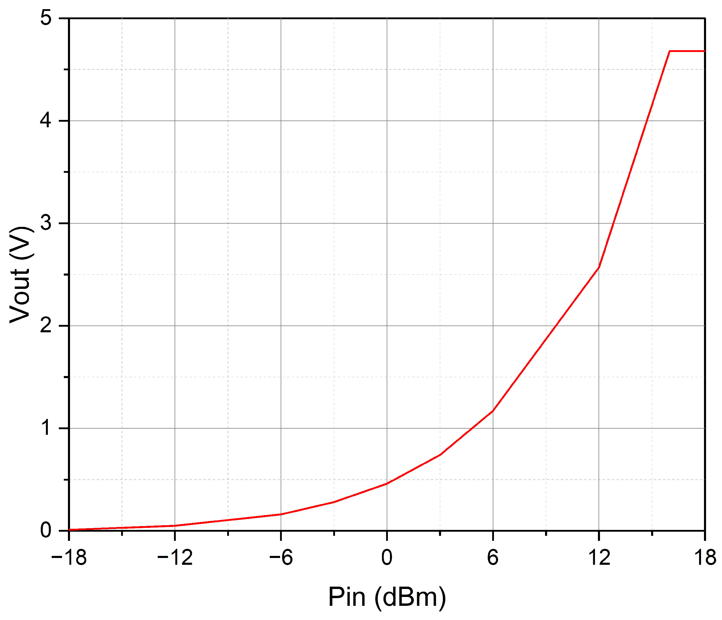
Figure 11 shows the output voltage of the proposed circuit versus the input power for an output load of 511 Ω . The output voltage is another important value that characterizes the rectifier circuit. Equation (5) gives the output voltage of the circuit:
V O U T = V O U T 1 V O U T 2 .
We observe that the larger output voltage is equal to 4.68 V for the input power 18 dBm. As the input power increases, so does the output voltage. Figure 11 shows that an input power larger than 6 dBm can give us an output voltage larger than 1 V. It should be noted that the power of 6 dBm is impossible or very difficult to obtain in practical Wi-Fi applications. So, this is a theoretical analysis to show the capabilities of the circuit from a purely electronic point of view.
Figure 12 shows the layout of the proposed quad-band rectifier circuit.

4.2. Performance Evaluation

Table 2 contains the relative measured results of the proposed rectifier circuit versus related circuits from the literature. The significant parameters that are nominated for the comparison are the type of circuit, the substrate of the circuit, the selected diodes, the frequencies of operation, the input power, the output load, the maximum power conversion efficiency, and the output voltage. From the results of the table, we can conclude that our rectifier circuit performs better than similar designs in the literature. It is designed on an RT/Duroid 5880 substrate and presents a fine-tuning operation in the frequency bands of interest. Furthermore, it has very good values at the tuning frequencies, and it adopts an impedance matching network technique with a relatively high complexity. Lastly, our rectifier circuit achieves satisfactory power conversion efficiency and high DC output voltage, which makes it a very good circuit for RF energy harvesting in Internet of Things (IoT) applications.

5. Discussion

During the last few years, the Internet of Things has attracted the attention of many researchers. A bibliographic search using the keywords “Internet of Things” and “RF Energy Harvesting” in the Scopus database shows that there are 180,169 articles related to the Internet of Things (IoT) and 5074 articles related to RF energy harvesting in the last 15 years.
The Internet of Things contains many physical devices connected through several networks and wireless systems. The use of batteries is challenging for many economic and environmental reasons. Alternative energy sources can complement or even better replace batteries. The RF energy that exists in the environment can resolve the energy issues in the wireless systems of an IoT network. This approach provides a consistent, clean, and green energy solution [6].
A rectenna is the main and appropriate system in RF energy harvesting. It comprises 4 subsystems, an antenna, a rectifier circuit, an impedance matching network, and a DC–DC converter [10,11]. These systems are designed to operate at frequencies that are important for wireless communications and broadcast services. The radio frequency range is part of the electromagnetic range that begins from VHF to EHF; the Wi-Fi band is also part of this range [12]. We designed a quad-band rectifier that works in the whole Wi-Fi band and, more specifically, at 2.4 , 3.5 , 5 , and 5.8 GHz. The main challenge we faced was the low RF power density that is available in the environment.
The role of the receiving antenna in a rectenna system is to collect as many RF signals as possible [10].
The rectifiers that convert RF signals into DC power can generally be categorized into integrated designs and discrete designs that use diodes or transistors [5,64]. We introduce a novel quad-band rectifier circuit that operates in the whole Wi-Fi range designed with distributed elements. This rectifier could be part of an IoT node to harvest environmental RF energy. The design procedure for the rectifier circuit comprises four main steps, which we presented and followed.
The proposed circuit is a Greinacher voltage multiplier based on the Delon voltage doubler topology [66]. This topology converts and amplifies AC input to DC output. The design was made on an RT/Duroid 5880 substrate [67] using HSMS-286C Schottky diodes [68]. The impedance matching network has two branches, one for 2.4 and 3.5 GHz and the other for 5 and 5.8 GHz. Each branch consists of a combination L and reverse L-shaped network with rectangular and radial stubs.
A high-gain DC–DC converter is applied as an interface circuit between the rectifier and the load to boost and stabilize the output of the rectifier [77,78].
To design and optimize the rectifier circuit, we used the gradient optimizer algorithm from the commercial software Advanced Design System (ADS) from Keysight Technologies. We found the impedance of the rectifier to be 52.62 i 0.16 , 49.31 i 4.28 , 47.84 i 1.25 , and 50.04 + i 0.86 at the four frequencies of operation ( 2.4 , 3.5 , 5 , 5.8 GHz). The S 11 is 31.85 , 27.22 , 31.86 , and 41.34 dB at the same frequencies, respectively. The operation bandwidth is 20 MHz at 2.4 GHz, 60 MHz at 3.49 GHz, 80 MHz at 4.99 GHz, and 59 MHz at 5.8 GHz. The initial design power conversion efficiency is 81.75 %, while the maximum output voltage is equal to 4.68 V. These results make this circuit a very good option for RF energy harvesting in Internet of Things (IoT) applications.
We introduced a novel quad-band rectifier featuring a new impedance matching network (IMN) and presented a comprehensive design framework. Our rectifier circuit operates simultaneously at four frequencies and outperforms similar designs. However, the circuit design has some limitations that could pose challenges for further development and practical application. Firstly, the circuit performs optimally at an input power of 12 dBm. Secondly, the matching circuit is complex, making adjustments difficult if it does not align well with the antenna. Additionally, it is important to note that our circuit outputs voltages exceeding 1 V when the input power is above 6 dBm. While this is promising from a theoretical electronic perspective, achieving 6 dBm in a typical Wi-Fi environment is challenging for wireless transmission.
In the future, our goal is to improve the power conversion efficiency and output voltage of the rectifier circuit. We also plan to fabricate the design for comparative analysis and integrate it into a larger project. Furthermore, we intend to develop an antenna to create a complete rectenna system.

6. Conclusions

In this work, we presented a novel quad-band RF-to-DC rectifier at 2.4 , 3.5 , 5 , and 5.8 GHz. The rectifier was designed on an RT/Duroid 5880 substrate. This circuit is suitable for working within the Wi-Fi band. Avago HSMS-286C diodes were used, while the Greinacher topology based on the Delon theory was selected. The circuit presents a PCE equal to 81.75 % and an output DC voltage equal to 4.68 V when the output load is 511 Ω , which can supply low-power electronics systems in IoT applications.

Author Contributions

Conceptualization, I.D.B. and M.S.P.; methodology, A.D.B.; software, S.S.; validation, I.D.B., A.D.B., and Z.D.Z.; formal analysis, I.D.B.; investigation, S.S.; resources, M.S.P.; data curation, M.S.P.; writing—original draft preparation, I.D.B.; writing—review and editing, S.K.G.; visualization, S.S.; supervision, S.K.G.; project administration, S.K.G.; funding acquisition, S.K.G. All authors have read and agreed to the published version of the manuscript.

Funding

This research received no external funding.

Institutional Review Board Statement

Not applicable.

Informed Consent Statement

Not applicable.

Data Availability Statement

The raw data supporting the conclusions of this article will be made available by the authors on request.

Conflicts of Interest

The authors declare no conflicts of interest.

References

  1. Singh, N.; Kanaujia, B.; Beg, M.; Mainuddin; Kumar, S.; Choi, H.C.; Kim, K.W. Low profile multiband rectenna for efficient energy harvesting at microwave frequencies. Int. J. Electron. 2019, 106, 2057–2071. [Google Scholar] [CrossRef]
  2. Valenta, C.R.; Durgin, G.D. Harvesting Wireless Power: Survey of Energy-Harvester Conversion Efficiency in Far-Field, Wireless Power Transfer Systems. IEEE Microw. Mag. 2014, 15, 108–120. [Google Scholar] [CrossRef]
  3. Zhang, J.; Hoare, D.; Das, R.; Holsgrove, M.; Czyzewski, J.; Mirzai, N.; Mercer, J.; Heidari, H. Wireless Impedance Platform for Autonomous Vascular Implantable Devices. In Proceedings of the 2022 29th IEEE International Conference on Electronics, Circuits and Systems (ICECS), Glasgow, UK, 24–26 October 2022; pp. 1–4. [Google Scholar] [CrossRef]
  4. Bonilla Licea, D.; Raza Zaidi, S.A.; McLernon, D.; Ghogho, M. Improving Radio Energy Harvesting in Robots Using Mobility Diversity. IEEE Trans. Signal Process. 2016, 64, 2065–2077. [Google Scholar] [CrossRef]
  5. Bougas, I.D.; Papadopoulou, M.S.; Psannis, K.; Sarigiannidis, P.; Goudos, S.K. State-of-the-art technologies in RF energy harvesting circuits—A review. In Proceedings of the 2020 IEEE 3rd World Symposium on Communication Engineering (WSCE), Thessaloniki, Greece, 9–11 October 2020; pp. 18–22. [Google Scholar]
  6. Niotaki, K.; Carvalho, N.B.; Georgiadis, A.; Gu, X.; Hemour, S.; Wu, K.; Matos, D.; Belo, D.; Pereira, R.; Figueiredo, R.; et al. RF Energy Harvesting and Wireless Power Transfer for Energy Autonomous Wireless Devices and RFIDs. IEEE J. Microwaves 2023, 3, 763–782. [Google Scholar] [CrossRef]
  7. Zhong, Y.W.; Yang, G.M.; Liu, Y.; Zheng, L.R. Optimal design of antenna array for multiple targets microwave power transmission with precise power division ratio control. IET Microwaves Antennas Propag. 2018, 12, 622–626. [Google Scholar] [CrossRef]
  8. Gowda, V.R.; Yurduseven, O.; Lipworth, G.; Zupan, T.; Reynolds, M.S.; Smith, D.R. Wireless Power Transfer in the Radiative Near Field. IEEE Antennas Wirel. Propag. Lett. 2016, 15, 1865–1868. [Google Scholar] [CrossRef]
  9. Wang, M.; Fan, Y.; Yang, L.; Li, Y.; Feng, J.; Shi, Y. Compact dual-band rectenna for RF energy harvest based on a tree-like antenna. IET Microwaves Antennas Propag. 2019, 13, 1350–1357. [Google Scholar] [CrossRef]
  10. Bougas, I.D.; Papadopoulou, M.S.; Boursianis, A.D.; Kokkinidis, K.; Goudos, S.K. State-of-the-art techniques in RF energy harvesting circuits. Telecom 2021, 2, 369–389. [Google Scholar] [CrossRef]
  11. Bougas, I.D.; Papadopoulou, M.S.; Boursianis, A.D.; Sarigiannidis, P.; Nikolaidis, S.; Goudos, S.K. Energy Harvesting & Autonomous Energy Systems: A Proposal for RF Energy Harvesting. In Proceedings of the 2024 13th International Conference on Modern Circuits and Systems Technologies (MOCAST), Sofia, Bulgaria, 26–28 June 2024; pp. 1–5. [Google Scholar] [CrossRef]
  12. Khan, N.U.; Khan, F.U.; Farina, M.; Merla, A. RF energy harvesters for wireless sensors, state of the art, future prospects and challenges: A review. Phys. Eng. Sci. Med. 2024, 47, 385–401. [Google Scholar] [CrossRef]
  13. Tentzeris, M.M.; Kawahara, Y. Novel Energy Harvesting Technologies for ICT Applications. In Proceedings of the 2008 International Symposium on Applications and the Internet, Washington, DC, USA, 28 July–1 August 2008; pp. 373–376. [Google Scholar] [CrossRef]
  14. Mann, S.; Cooper, T.; Allen, S.; Blackwell, R.; Lowe, A. Exposure to radio waves near mobile phone base stations. Radiol. Prot. Bull. 2000, 4, 13–16. [Google Scholar]
  15. Bougas, I.D.; Papadopoulou, M.S.; Boursianis, A.D.; Nikolaidis, S.; Goudos, S.K. Dual-Band Rectifier Circuit Design for IoT Communication in 5G Systems. Technologies 2023, 11, 34. [Google Scholar] [CrossRef]
  16. Ibrahim, H.H.; Singh, M.J.; Al-Bawri, S.S.; Ibrahim, S.K.; Islam, M.T.; Alzamil, A.; Islam, M.S. Radio frequency energy harvesting technologies: A comprehensive review on designing, methodologies, and potential applications. Sensors 2022, 22, 4144. [Google Scholar] [CrossRef] [PubMed]
  17. De Vito, L.; Cocca, V.; Riccio, M.; Tudosa, I. Wireless Active Guardrail System for environmental measurements. In Proceedings of the 2012 IEEE Workshop on Environmental Energy and Structural Monitoring Systems (EESMS), Perugia, Italy, 28 September 2012; pp. 50–57. [Google Scholar] [CrossRef]
  18. Chen, C.; Jiang, J.; Zhou, Y.; Lv, N.; Liang, X.; Wan, S. An edge intelligence empowered flooding process prediction using Internet of things in smart city. J. Parallel Distrib. Comput. 2022, 165, 66–78. [Google Scholar] [CrossRef]
  19. Chen, C.; Li, H.; Li, H.; Fu, R.; Liu, Y.; Wan, S. Efficiency and Fairness Oriented Dynamic Task Offloading in Internet of Vehicles. IEEE Trans. Green Commun. Netw. 2022, 6, 1481–1493. [Google Scholar] [CrossRef]
  20. Liu, S.; Yu, J.; Deng, X.; Wan, S. FedCPF: An Efficient-Communication Federated Learning Approach for Vehicular Edge Computing in 6G Communication Networks. IEEE Trans. Intell. Transp. Syst. 2022, 23, 1616–1629. [Google Scholar] [CrossRef]
  21. Lu, J.; Liu, H.; Zhang, Z.; Wang, J.; Goudos, S.K.; Wan, S. Toward Fairness-Aware Time-Sensitive Asynchronous Federated Learning for Critical Energy Infrastructure. IEEE Trans. Ind. Inform. 2022, 18, 3462–3472. [Google Scholar] [CrossRef]
  22. What Are WiFi Bands and How Many Do I Need for My Network? Available online: https://kb.netgear.com/000064790/What-are-WiFi-bands-and-how-many-do-I-need-for-my-network (accessed on 20 August 2024).
  23. Kuhn, V.; Seguin, F.; Lahuec, C.; Person, C. Enhancing RF-to-DC conversion efficiency of wideband RF energy harvesters using multi-tone optimization technique. Int. J. Microw. Wirel. Technol. 2016, 8, 143–153. [Google Scholar] [CrossRef]
  24. Yong, J.K.; Lian, W.X.; Ramiah, H.; Churchill, K.K.P.; Chong, G.; Lai, N.S.; Chen, Y.; Mak, P.I.; Martins, R.P. A Fully Integrated CMOS Tri-Band Ambient RF Energy Harvesting System for IoT Devices. IEEE Trans. Circuits Syst. I Regul. Pap. 2023, 70, 4705–4718. [Google Scholar] [CrossRef]
  25. Dehghani, S.; Johnson, T. A 2.4-GHz CMOS Class-E Synchronous Rectifier. IEEE Trans. Microw. Theory Tech. 2016, 64, 1655–1666. [Google Scholar] [CrossRef]
  26. Chatterjee, S.; Tarique, M. A 100-nW Sensitive RF-to-DC CMOS Rectifier for Energy Harvesting Applications. In Proceedings of the 2016 29th International Conference on VLSI Design and 2016 15th International Conference on Embedded Systems (VLSID), Kolkata, India, 4–8 January 2016; pp. 557–558. [Google Scholar] [CrossRef]
  27. Jantarachote, V.; Tontisirin, S.; Akkaraekthalin, P.; Negra, R.; Chalermwisutkul, S. CMOS rectifier design for RFID chip with high sensitivity at low input power to be combined with an ultrasmall antenna. Int. J. Numer. Model. Electron. Netw. Devices Fields 2019, 32, e2607. [Google Scholar] [CrossRef]
  28. Rosli, M.; Murad, S.; Norizan, M.; Ramli, M. Design of RF to DC conversion circuit for energy harvesting in CMOS 0.13-μm technology. AIP Conf. Proc. 2018, 2045, 020089. [Google Scholar] [CrossRef]
  29. Lo, Y.L.; Chuang, Y.H. A High-Efficiency CMOS Rectifier with Wide Harvesting Range and Wide Band Based on MPPT Technique for Low-Power IoT System Applications. Circuits Syst. Signal Process. 2017, 36, 5019–5040. [Google Scholar] [CrossRef]
  30. Basim, M.; Khan, D.; Ain, Q.U.; Shehzad, K.; Shah, S.A.A.; Jang, B.G.; Pu, Y.G.; Yoo, J.M.; Kim, J.T.; Lee, K.Y. A Highly Efficient RF-DC Converter for Energy Harvesting Applications Using a Threshold Voltage Cancellation Scheme. Sensors 2022, 22, 2659. [Google Scholar] [CrossRef] [PubMed]
  31. Yoshida, S.; Fukuda, G.; Kobayashi, Y.; Tashiro, S.; Noji, T.; Nishikawa, K.; Kawasaki, S. The C-band MPT rectifierusing a HEMT without bonding-wire connection for a space health monitoring system. In Proceedings of the 2013 IEEE Wireless Power Transfer (WPT), Perugia, Italy, 15–16 May 2013; pp. 163–166. [Google Scholar] [CrossRef]
  32. Jung, Y.H.; Zhang, H.; Lee, I.K.; Shin, J.H.; Kim, T.i.; Ma, Z. Releasable high-performance GaAs Schottky diodes for gigahertz operation of flexible bridge rectifier. Adv. Electron. Mater. 2019, 5, 1800772. [Google Scholar] [CrossRef]
  33. Bougas, I.D.; Papadopoulou, M.S.; Boursianis, A.D.; Sarigiannidis, P.; Nikolaidis, S.; Goudos, S.K. Rectifier circuit design for 5G energy harvesting applications. In Proceedings of the 2022 11th International Conference on Modern Circuits and Systems Technologies (MOCAST), Bremen, Germany, 8–10 June 2022; pp. 1–4. [Google Scholar] [CrossRef]
  34. Sarma, S.S.; Chandravanshi, S.; Akhtar, M.J. Triple band differential rectifier for RF energy harvesting applications. In Proceedings of the 2016 Asia-Pacific Microwave Conference (APMC), New Delhi, India, 5–9 December 2016; pp. 1–4. [Google Scholar] [CrossRef]
  35. Zied, C.M.; Rashid, E.R.; Hareb, A. Harvesting microwave energy from WiMax bands based on a Dual-Band Antenna. IOP Conf. Ser. Earth Environ. Sci. 2019, 227, 042044. [Google Scholar] [CrossRef]
  36. Derbal, M.C.; Nedil, M. A high gain dual band rectenna for RF energy harvesting applications. Prog. Electromagn. Res. Lett. 2020, 90, 29–36. [Google Scholar] [CrossRef]
  37. Dardeer, O.M.A.; Elsadek, H.A.; Abdallah, E.A. Compact Broadband Rectenna for Harvesting RF Energy in WLAN and WiMAX Applications. In Proceedings of the 2019 International Conference on Innovative Trends in Computer Engineering (ITCE), Aswan, Egypt, 2–4 February 2019; pp. 292–296. [Google Scholar] [CrossRef]
  38. Eltresy, N.; Eisheakh, D.; Abdallah, E.; Elhenawy, H. RF Energy Harvesting Using Efficiency Dual Band Rectifier. In Proceedings of the 2018 Asia-Pacific Microwave Conference (APMC), Kyoto, Japan, 6–9 November 2018; pp. 1453–1455. [Google Scholar] [CrossRef]
  39. Saravanan, M.; Priya, A. Design of tri-band microstrip patch rectenna for radio frequency energy harvesting system. IETE J. Res. 2022, 68, 2410–2415. [Google Scholar] [CrossRef]
  40. Chandravanshi, S.; Sarma, S.S.; Akhtar, M.J. Design of Triple Band Differential Rectenna for RF Energy Harvesting. IEEE Trans. Antennas Propag. 2018, 66, 2716–2726. [Google Scholar] [CrossRef]
  41. Azam, S.K.; Islam, M.S.; Hossain, A.; Othman, M. Monopole antenna on transparent substrate and rectifier for energy harvesting applications in 5G. Int. J. Adv. Comput. Sci. Appl. 2020, 11, 84–89. [Google Scholar] [CrossRef]
  42. Usman, M.; Khan, W.T. Six Band RF Energy Harvesting From Ambient Signals. 2019. Available online: https://www.mtt.org/app/uploads/2019/01/10-Final-Report_Usman.pdf (accessed on 20 August 2024).
  43. Mohd Noor, F.S.; Zakaria, Z.; Lago, H.; Meor Said, M.A. Dual-band aperture-coupled rectenna for radio frequency energy harvesting. Int. J. Microw. Comput. Aided Eng. 2019, 29, e21651. [Google Scholar] [CrossRef]
  44. Mirzababaee, N.; Geran, F.; Mohanna, S. A radio frequency energy harvesting rectenna for GSM, LTE, WLAN, and WiMAX. Int. J. Microw. Comput. Aided Eng. 2021, 31, e22630. [Google Scholar] [CrossRef]
  45. Reed, R.; Pour, F.L.; Ha, D.S. An Efficient 2.4 GHz Differential Rectenna for Radio Frequency Energy Harvesting. In Proceedings of the 2020 IEEE 63rd International Midwest Symposium on Circuits and Systems (MWSCAS), Springfield, MA, USA, 9–12 August 2020; pp. 208–212. [Google Scholar] [CrossRef]
  46. Gabriel, K.; Fayrouz, H.; Nessakh, B.; Wenceslas, R.; Sawsan, S. 2.45GHz Low-Power Diode Bridge Rectifier Design. In Proceedings of the 2023 International Conference on Microelectronics (ICM), Abu Dhabi, United Arab Emirates, 17–20 December 2023; pp. 268–271. [Google Scholar] [CrossRef]
  47. Hamzi, I.; Bakkali, M.E.; Aghoutane, M.; Touhami, N.A. Conversion Efficiency Study of the Bridge Rectifier at 2.4 GHz. Procedia Manuf. 2020, 46, 771–776, In Proceedings of the 13th International Conference Interdisciplinarity in Engineering, INTER-ENG 2019, Targu Mures, Romania, 3–4 October 2019. [Google Scholar] [CrossRef]
  48. Samakkhee, W.; Phaebua, K.; Lertwiriyaprapa, T. 5.8 GHz rectifier circuit for electromagnetic energy harvesting system. In Proceedings of the 2017 International Symposium on Antennas and Propagation (ISAP), Phuket, Thailand, 30 October–2 November 2017; pp. 1–2. [Google Scholar] [CrossRef]
  49. Ben Yamna, M.; Dakhli, N.; Sakli, H. Rectifier Circuit at 3.5 GHz for 5G Applications. In Proceedings of the 2022 IEEE 21st international Ccnference on Sciences and Techniques of Automatic Control and Computer Engineering (STA), Sousse, Tunisia, 19–21 December 2022; pp. 305–309. [Google Scholar] [CrossRef]
  50. Lee, H.; Lee, J.C. Optimization of a 5.8-GHz rectifier considering ripple amplitude and DC-voltage pattern. In Proceedings of the 2014 IEEE Wireless Power Transfer Conference, Jeju Island, Republic of Korea, 8–9 May 2014; pp. 212–215. [Google Scholar] [CrossRef]
  51. Huang, R.; Ren, W.; Deng, X. Design of a 5.8 GHz Rectifier Circuit for Wireless Power Transfer Applications. In Proceedings of the 2021 2nd International Conference on Artificial Intelligence and Information Systems, Chongqing, China, 28–30 May 2021; pp. 1–4. [Google Scholar]
  52. Bae, J.; Yi, S.H.; Choi, W.; Koo, H.; Hwang, K.C.; Lee, K.Y.; Yang, Y. 5.8 GHz high-efficiency RF–DC converter based on common-ground multiple-stack structure. Sensors 2019, 19, 3257. [Google Scholar] [CrossRef]
  53. Khaliq, H.S.; Awais, M.; Ahmad, W.; Khan, W.T. A high gain six band frequency independent dual CP planar log periodic antenna for ambient RF energy harvesting. In Proceedings of the 2017 Progress in Electromagnetics Research Symposium—Fall (PIERS—FALL), Singapore, 19–22 November 2017; pp. 3024–3028. [Google Scholar] [CrossRef]
  54. Saghlatoon, H.; Björninen, T.; Sydänheimo, L.; Tentzeris, M.M.; Ukkonen, L. Inkjet-printed wideband planar monopole antenna on cardboard for RF energy-harvesting applications. IEEE Antennas Wirel. Propag. Lett. 2014, 14, 325–328. [Google Scholar] [CrossRef]
  55. Khang, S.T.; Yu, J.W.; Lee, W.S. Compact folded dipole rectenna with RF-based energy harvesting for IoT smart sensors. Electron. Lett. 2015, 51, 926–928. [Google Scholar] [CrossRef]
  56. Gravas, I.P.; Sifakis, N.F.; Zaharis, Z.D.; Lazaridis, P.I.; Xenos, T.D. Optimal Fractal Antenna for In-Vehicle Entertainment Application. In Proceedings of the 2020 Wireless Telecommunications Symposium (WTS), Washington, DC, USA, 22–24 April 2020; pp. 1–5. [Google Scholar] [CrossRef]
  57. Hu, Y.Y.; Sun, S.; Xu, H. Compact Collinear Quasi-Yagi Antenna Array for Wireless Energy Harvesting. IEEE Access 2020, 8, 35308–35317. [Google Scholar] [CrossRef]
  58. Congedo, F.; Monti, G.; Tarricone, L.; Cannarile, M. Broadband bowtie antenna for RF energy scavenging applications. In Proceedings of the 5th European Conference on Antennas and Propagation (EUCAP), Rome, Italy, 11–15 April 2011; pp. 335–337. [Google Scholar]
  59. Kamoda, H.; Kitazawa, S.; Kukutsu, N.; Kobayashi, K. Loop Antenna Over Artificial Magnetic Conductor Surface and Its Application to Dual-Band RF Energy Harvesting. IEEE Trans. Antennas Propag. 2015, 63, 4408–4417. [Google Scholar] [CrossRef]
  60. Agrawal, S.; Gupta, R.D.; Parihar, M.S.; Kondekar, P.N. A wideband high gain dielectric resonator antenna for RF energy harvesting application. AEU Int. J. Electron. Commun. 2017, 78, 24–31. [Google Scholar] [CrossRef]
  61. Shen, S.; Zhang, Y.; Chiu, C.Y.; Murch, R. An Ambient RF Energy Harvesting System Where the Number of Antenna Ports is Dependent on Frequency. IEEE Trans. Microw. Theory Tech. 2019, 67, 3821–3832. [Google Scholar] [CrossRef]
  62. Shen, S.; Chiu, C.Y.; Murch, R.D. A Dual-Port Triple-Band L-Probe Microstrip Patch Rectenna for Ambient RF Energy Harvesting. IEEE Antennas Wirel. Propag. Lett. 2017, 16, 3071–3074. [Google Scholar] [CrossRef]
  63. Saen, T.; Itoh, K.; Betsudan, S.i.; Makino, S.; Hirota, T.; Noguchi, K.; Shimozawa, M. Fundamentals of the bridge RF rectifier with an impedance transformer. In Proceedings of the 2011 IEEE MTT-S International Microwave Workshop Series on Innovative Wireless Power Transmission: Technologies, Systems, and Applications, Kyoto, Japan, 12–13 May 2011; pp. 255–258. [Google Scholar] [CrossRef]
  64. Park, J.; Kim, Y.; Yoon, Y.J.; So, J.; Shin, J. Rectifier design using distributed Greinacher voltage multiplier for high frequency wireless power transmission. J. Electromagn. Eng. Sci. 2014, 14, 25–30. [Google Scholar] [CrossRef]
  65. Ohira, T. Power efficiency and optimum load formulas on RF rectifiers featuring flow-angle equations. IEICE Electron. Express 2013, 10, 20130230. [Google Scholar] [CrossRef]
  66. Delon Voltage Multiplier, or How to Double or Triple Transformer Voltage. Available online: https://www.jurasz.de/en/jarek/delon (accessed on 20 August 2024).
  67. RT/Duroid ®5870/5880: High Frequency Laminates. Available online: https://rogerscorp.com/-/media/project/rogerscorp/documents/advanced-electronics-solutions/english/data-sheets/rt-duroid-5870—5880-data-sheet.pdf (accessed on 20 August 2024).
  68. Merabet, B.; Cirio, L.; Takhedmit, H.; Costa, F.; Vollaire, C.; Allard, B.; Picon, O. Low-cost converter for harvesting of microwave electromagnetic energy. In Proceedings of the 2009 IEEE Energy Conversion Congress and Exposition, San Jose, CA, USA, 20–24 September 2009; pp. 2592–2599. [Google Scholar] [CrossRef]
  69. El Mattar, S.; Baghdad, A. High-efficiency 2.45 and 5.8 GHz dual-band rectifier design with modulated input signals and a wide input power range. Int. J. Electr. Comput. Eng. 2023, 13, 2088–8708. [Google Scholar] [CrossRef]
  70. Liu, D.S.; Li, F.B.; Zou, X.C.; Liu, Y.; Hui, X.M.; Tao, X.F. New analysis and design of a RF rectifier for RFID and implantable devices. Sensors 2011, 11, 6494–6508. [Google Scholar] [CrossRef]
  71. Takhedmit, H.; Merabet, B.; Cirio, L.; Allard, B.; Costa, F.; Vollaire, C.; Picon, O. A 2.45-GHz dual-diode RF-to-dc rectifier for rectenna applications. In Proceedings of the 40th European Microwave Conference, Paris, France, 28–30 September 2010; pp. 37–40. [Google Scholar] [CrossRef]
  72. HSMS-286x Series: Surface Mount Microwave Schottky Detector Diodes. Available online: https://gr.mouser.com/datasheet/2/678/V02_1388EN0-1222339.pdf (accessed on 20 August 2024).
  73. Deng, X.; Yang, P.; Chen, S.; Ren, W. Design of a 2.4 & 5.8 GHz Efficient Circularly Polarized Rectenna for Wireless Power Transfer Applications. Electronics 2023, 12, 2645. [Google Scholar] [CrossRef]
  74. Yue, X.; Du, S. A 2-Mode Reconfigurable SSHI Rectifier with 3.2X Lower Cold-Start Requirement for Piezoelectric Energy Harvesting. In Proceedings of the 2022 29th IEEE International Conference on Electronics, Circuits and Systems (ICECS), Glasgow, UK, 24–26 October 2022; pp. 1–4. [Google Scholar] [CrossRef]
  75. AN5457: RF Matching Network Design Guide for STM32WL Series. Available online: https://www.st.com/resource/en/application_note/an5457-rf-matching-network-design-guide-for-stm32wl-series-stmicroelectronics.pdf (accessed on 20 August 2024).
  76. Singh, N.; Kanaujia, B.K.; Tariq Beg, M.; Mainuddin.; Kumar, S. A triple band circularly polarized rectenna for RF energy harvesting. Electromagnetics 2019, 39, 481–490. [Google Scholar] [CrossRef]
  77. Roberts, S. DC/DC Book of Knowledge: Practical Tips for the User; Recom: Singapore, 2015. [Google Scholar]
  78. Shayeghi, H.; Pourjafar, S.; Hashemzadeh, S.; Sedaghati, F. A dc-dc converter with high voltage conversion ratio recommended for renewable energy application. J. Oper. Autom. Power Eng. 2024, 12, 186–194. [Google Scholar]
  79. Zeng, M.; Andrenko, A.S.; Liu, X.; Zhu, B.; Li, Z.; Tan, H.Z. Differential topology rectifier design for ambient wireless energy harvesting. In Proceedings of the 2016 IEEE International Conference on RFID Technology and Applications (RFID-TA), Foshan, China, 21–23 September 2016; pp. 97–101. [Google Scholar] [CrossRef]
  80. Cansiz, M.; Altinel, D.; Kurt, G.K. Efficiency in RF energy harvesting systems: A comprehensive review. Energy 2019, 174, 292–309. [Google Scholar] [CrossRef]
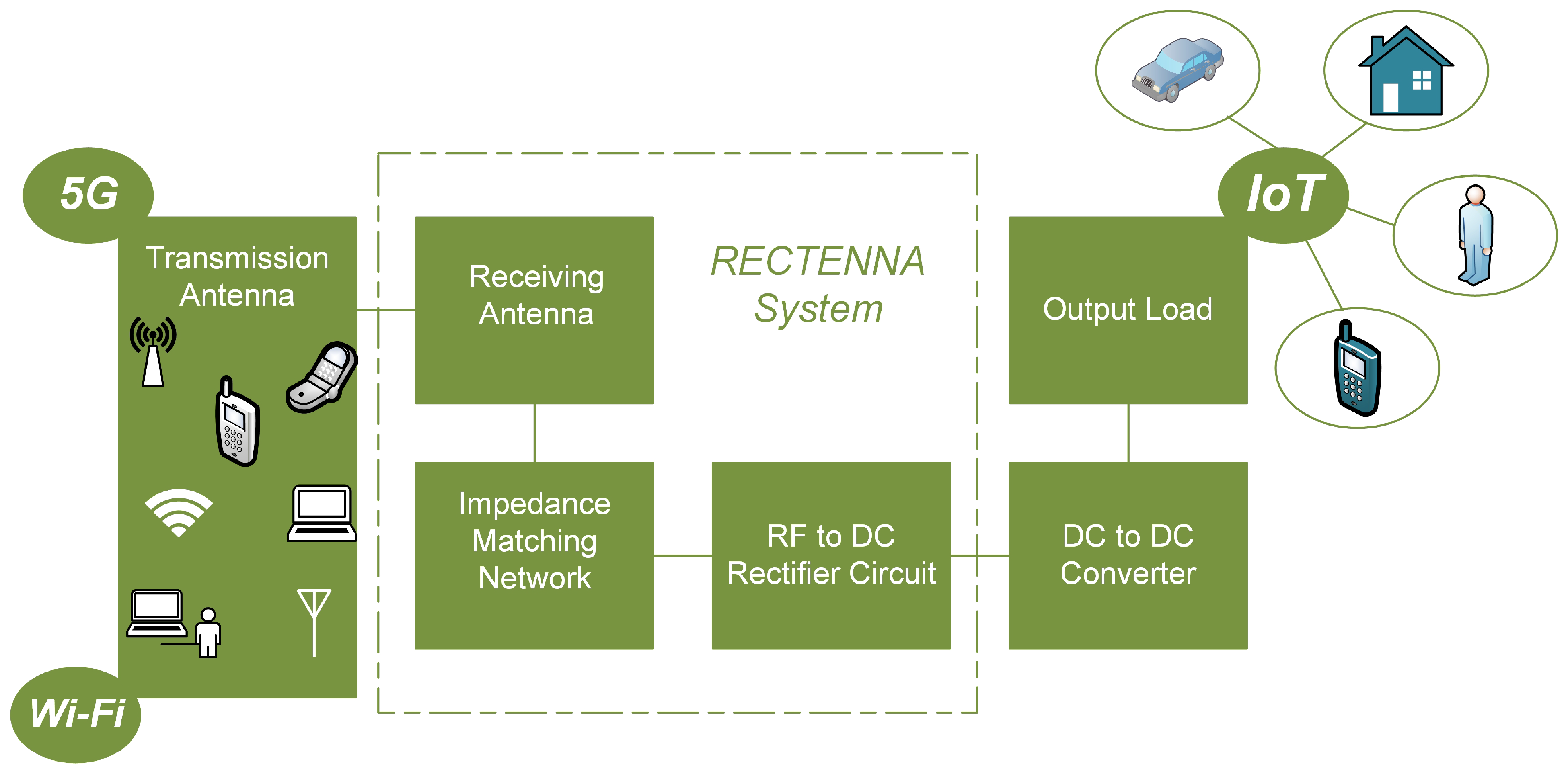
Figure 1. Typical RF energy harvesting system.
Technologies 12 00188 g001
Figure 2. Methodology.
Technologies 12 00188 g002
Figure 3. Greinacher voltage multiplier.
Technologies 12 00188 g003
Figure 4. Voltage multiplier.
Technologies 12 00188 g004
Figure 5. Substrate.
Technologies 12 00188 g005
Figure 6. Impedance matching network.
Technologies 12 00188 g006
Figure 7. Quad-band rectifier.
Technologies 12 00188 g007
Figure 8. S 11 Reflection coefficient.
Technologies 12 00188 g008
Figure 9. PCE versus R L .
Technologies 12 00188 g009
Figure 10. (PCE) Power conversion efficiency versus P i n (input power).
Technologies 12 00188 g010
Figure 11. Output voltage versus input power.
Technologies 12 00188 g011
Figure 12. Layout of the quad-band rectifier.
Technologies 12 00188 g012
Table 1. Physical parameters.
ParameterWidth/LengthAngle
TL12/30 mm-
TL22/13 mm-
TL32/3 mm-
TL42/ 9.5 mm-
TL52/ 7.5 mm-
TL61/ 4.5 mm-
TL72/13 mm-
TL82/ 7.5 mm-
TL92/ 2.5 mm-
TL102/14 mm-
TL111/ 1.5 mm-
TL12 4.2 / 9.3 mm-
STUB1200 nm/ 5.2  mm 61.5 degrees
STUB23/5 mm 69.7 degrees
STUB3200 nm/6 mm 20.8 degrees
Table 2. Comparative results between the proposed quad-band rectifier and related work.
ReferenceType of Circuit (+)SubstrateDiodeFrequency (GHz) P in (dBm) R L (kΩ)PCE (%) @ Desired Frequencies V out
[1]Full-wave rectifier +FR-4HSMS-2820C 0.9 , 1.8 , 2.5 , 3.5 , 5.5 , 7.35 --788 (@3.5 GHz) V
[9]Full-wave rectifierFR-4HSMS-2852 2.45 , 3.50 0 1.20 68.40 (@2.45 GHz), 62.20 (@2.45 GHz) 1.22  V
[15]Full-wave rectifierRT/Duroid 5880HSMS-286C 3.5 , 512 1.74 53 3.815  V
[31]Full-wave rectifier +-- 5.1 15 0.350 51.3 -
[32]Full-wave rectifier +-Gallium Arsenide printed diodes5-- 36.4 -
[33]Full-wave rectifierRT/Duroid 5880HSMS-286C 3.5 9 1.1 42.5 -
[34]Full-wave rectifier +FR-4HSMS-286C 1.9 2.5 , 3.6 14342 5.53  V
[35]Full-wave rectifier +FR-4HSMS-2820 2.45 , 3.8 20 0.230 64.3 4.23  V
[36]Half-wave rectifier +RT/Duroid 5880SMS-7630 3.5 , 5.8 0 0.5 44656.88 mV
[37]Full-wave rectifierFR-4HSMS-2860 3.5 61 29.7 2.80  V
[38]Half-wave rectifierFR-4SMS-7630 2.4 , 3.5 0- 61.6 -
[39]Full-wave rectifier +FR-4NXP BAP50-03 2.4 , 4, 5--54 (@ 2.4  GHz)298 (@2.4 GHz) mV
[40]Full-wave rectifierFR-4HSMS-285C2, 2.5 , 3.5 2 1.1 61-
[41]Full-wave rectifierRogers RO3003SMS-7630-079 LF 3.51 0242-
[42]Full-wave rectifier-SMS-7630 0.9 , 1.8 , 2.1 , 2.4 , 5 15 - 33.5 (@ 1.8  GHz) 0.5  V
[43]Full-wave rectifierFR-4HSMS-286B 2.45 , 50 0.70 68.83 0.236  V
[44]Full-wave rectifier +RT/Duroid 5880SMS-7630 0.84 , 1.29 , 1.68 , 3.08 , 3.45 , 4.31 , 5.11 , 5.49 05 45.69 (@ 3.45  GHz)-
[45]Full-wave rectifier +RO4003CSMS-7630 2.4 5.5 2 69.3 -
[46]Full-wave rectifierRO4350BSMS-7630, HSMS-2850 2.4 5 357-
[47]Full-wave rectifier-HSMS-2850 2.4 10 1.4 80-
[48]Full-wave rectifier +-SMS-7630-061 5.8 10--3 V
[49]Half-wave rectifierFR-4HSMS-2860 3.5 02 63.5 2.50  V
[50]--HSMS-286B 5.8 9 1.3 72-
[51]Full-wave rectifier-HSMS-285C 5.8 3.6 10.5 1.7 60 3.5  V
[52]Full-wave rectifier +-MA4E1319-1 5.8 214 73.1 34.2  V
This WorkFull-wave rectifierRT/Duroid 5880HSMS-286C 2.4 , 3.5 , 5, 5.8 12 0.511 81.75 4.68  V (@18 dBm)
+ Results of fabricated circuit.
Disclaimer/Publisher’s Note: The statements, opinions and data contained in all publications are solely those of the individual author(s) and contributor(s) and not of MDPI and/or the editor(s). MDPI and/or the editor(s) disclaim responsibility for any injury to people or property resulting from any ideas, methods, instructions or products referred to in the content.