1. Introduction
Unmanned Aerial Systems (UAS) are being proposed for numerous exciting applications. These applications range from the classic military strike, surveillance, and reconnaissance operations to newer proposed uses such as scientific measurement in extreme environments, weather pattern tracking, rangeland imaging and analysis, and even shipping of small goods [
1,
2,
3,
4]. The UAS design can offer many advantages over the conventional manned configuration including reduced size and weight costs, eliminated onboard pilot risk, and a larger operation envelope into biologically hazardous conditions. However, as with all engineering designs, these advantages usually come with a tradeoff. The immediately obvious tradeoff is the loss of human control inside the aircraft. Although it can be argued that this is not necessarily a drawback considering how robust wireless and autonomous systems have become, many people are uncomfortable with the idea of remote operation or autonomous control of aircraft in certain applications, and the communication links and autonomous control are not foolproof; then again, neither is manned control. It will be interesting to see how these attitudes shift in the coming decades as the technology progresses.
The typical UAS design process is remarkably similar to the design process of a conventional manned aircraft. It consists of the typical balancing act between the various design components: structures, aerodynamics, propulsion, weights and balancing, avionics, stability and control, etc. The design begins to become more well-defined as it moves from the conceptual to the preliminary stage, and finally to the detailed design. The major aerodynamic and structural decisions are made in the preliminary stage, whereas the antenna and avionics systems are typically not well-defined until the preliminary or even the detailed design stages. This antenna design delay results in overall designs where the antennas are pushed to secondary consideration. The goal of this study is to pull the antenna design to the forefront of the preliminary design stage in the hopes of developing a novel, aerodynamically functionalized wideband antenna.
Much work has been devoted to integrate antennas into the structure of aircraft to mitigate drag and weight penalties. Blade antennas utilize broadband monopoles embedded in aerodynamic external coatings [
5]. The bandwidth can be further enhanced in conjunction with tunable matching networks. Another approach is to use characteristic mode analysis, an eigenmode solution technique, to examine the coupling of various antennas to the external skin of vehicles and create an integrated electromagnetic/aerodynamic topology to optimize some electromagnetic performance criterion [
6,
7,
8]. There has also been recent work in developing new conformal, low-profile antennas such as annular slot antennas [
9]. All of these studies take the majority of the aerodynamic structure as a fixed or semi-fixed design point before starting the electromagnetics analysis. The novelty of this work lies in taking a canonical antenna geometry as the starting point and developing it into a fully realizable UAS.
2. Antenna Design
The desired antenna performance metrics include:
- (1)
Wideband impedance match from 100 MHz to upwards of 2 GHz
- (2)
Conformal, lightweight structure to minimize weight and drag penalty
- (3)
Large surface for mounting various sensor networks and flight components
The first condition ensures that the antenna will operate with minimum reflections from the feed excitation over a wide frequency range. The large frequency range allows for greater electromagnetic and operational flexibility as well as for advanced large bandwidth communication protocols. The second condition becomes important so as not to constrain the aerodynamic design to an unachievable design point. Larger surfaces allow for greater bandwidths and allowing nonconformal antennas would increase the permissible antenna design space, but the aircraft design requires a careful accounting of weight and drag penalties. Satisfaction of the third condition permits mission flexibility and modularity.
The desired lightweight, conformal antenna characteristics along with the first wide impedance bandwidth immediately prompted the selection of a planar dipole or Vivaldi traveling wave structure. These antennas are planar, can achieve impedance bandwidths larger than 20:1, and can be made lightweight with proper selection of substrate and metallization materials [
10,
11,
12,
13,
14,
15]. These structures can be understood by the slot-line transmission line from which they are based. The fields of a typical slot-line are tightly bound to the conductors due to the small electrical length between the conductors. As the slot becomes electrically wider, the fields become less bound to the conductors and begin to radiate. The total field is the summation of a traveling wave down the transmission line and a radiated field. The point along the slot-line at which radiation occurs for a particular frequency is determined by the slot in terms of electrical length. Higher frequencies will radiate at a smaller slot width and lower frequencies will radiate at larger slot widths. This mechanism allows these antennas to achieve large bandwidths.
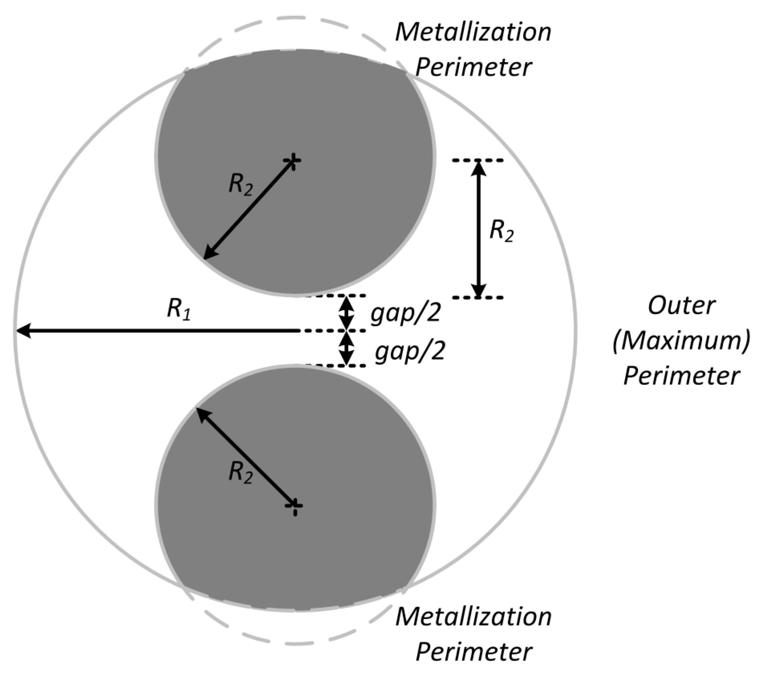
Figure 1 shows the proposed antenna geometry. The configuration consists of geometrically circular conductors separated by a gap distance and placed atop a dielectric substrate. The planar geometry is fully defined by three parameters:
R1 determines the outer boundary of the dielectric substrate;
R2 determines the metallization geometry;
Gap specifies the distance between conductors for gap feed.
Figure 1.
Proposed antenna geometry.
Figure 1.
Proposed antenna geometry.
The metallization area is defined by the intersection of a circle of radius R
2 offset by a distance of
R2 from the gap edge with the primary circle of radius
R1.
Figure 2 illustrates the effect of increasing
R2 on the metallization geometry with an
R1 value of 24′′. The metallization for the
R2 = 24′′ case shows a classical circular planar dipole, whereas higher
R2 values result in metallizations indicative of tapered slotline antennas with smaller slot areas.
Figure 2.
Metallization geometry as a function of R2 (R1 = 24′′).
Figure 2.
Metallization geometry as a function of R2 (R1 = 24′′).
An R1 value of 24′′ was chosen as a compromise between an extremely large aerodynamic structure, which will require an unreasonably large powerplant for flight, and a smaller structure which will have largely capacitive impedances at lower frequencies. The chosen substrate material was 4 mm thick Rohacell foam. Rohacell is widely used in the RF industry due to its low dielectric constant of 1.1 and small losses (tanδ < 10−4).
The first step in the design process was to simulate the geometries depicted in
Figure 1 and examine the impedance match behavior of the antennas for the low end of the desired frequency band from 50 MHz to 500 MHz. All simulations were conducted in High Frequency Structural Simulator (HFSS), a full-wave finite element software package. The feed was simulated as a lumped port with an assigned impedance of 50 Ω.
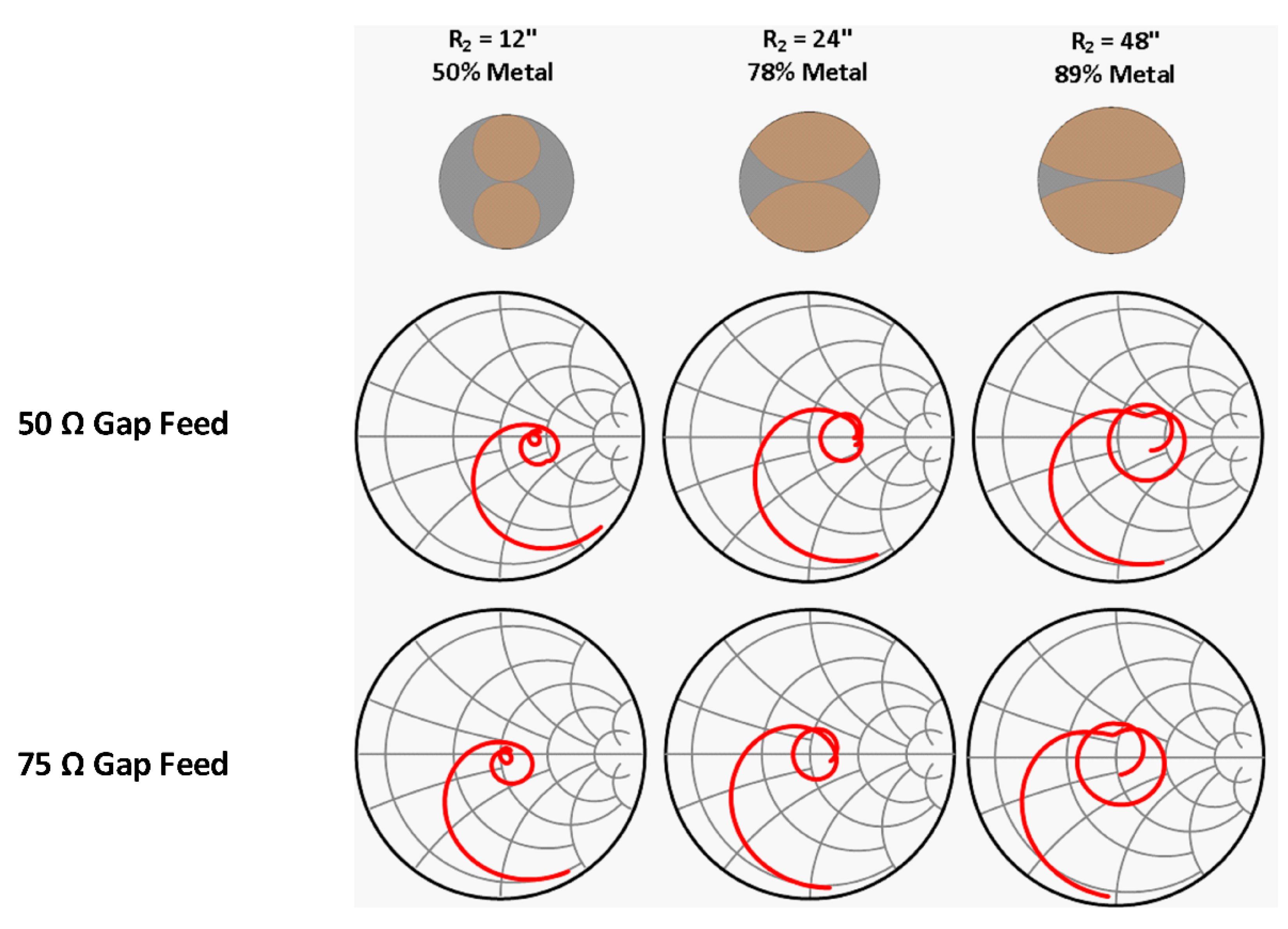
Figure 3 shows the impedance behavior results of the simulations. All metallization cases achieve a reasonable match, but the 50 Ω feed causes the antennas to achieve the best match at a normalized impedance value of 1.5. This normalized value indicates that a better match would be achieved with a feed impedance of 75 Ω. The simulations were conducted again with a new feed impedance of 75 Ω, and the results are shown below in
Figure 3. The new 75 Ω feed impedance results in a better match. Also, the
R2 = 12′′ metallization case reaches this matched point at the lowest frequency of all the metallization cases. Therefore, further designs were based upon this metallization geometry.
Figure 3.
Impedance behavior of metallization cases.
Figure 3.
Impedance behavior of metallization cases.
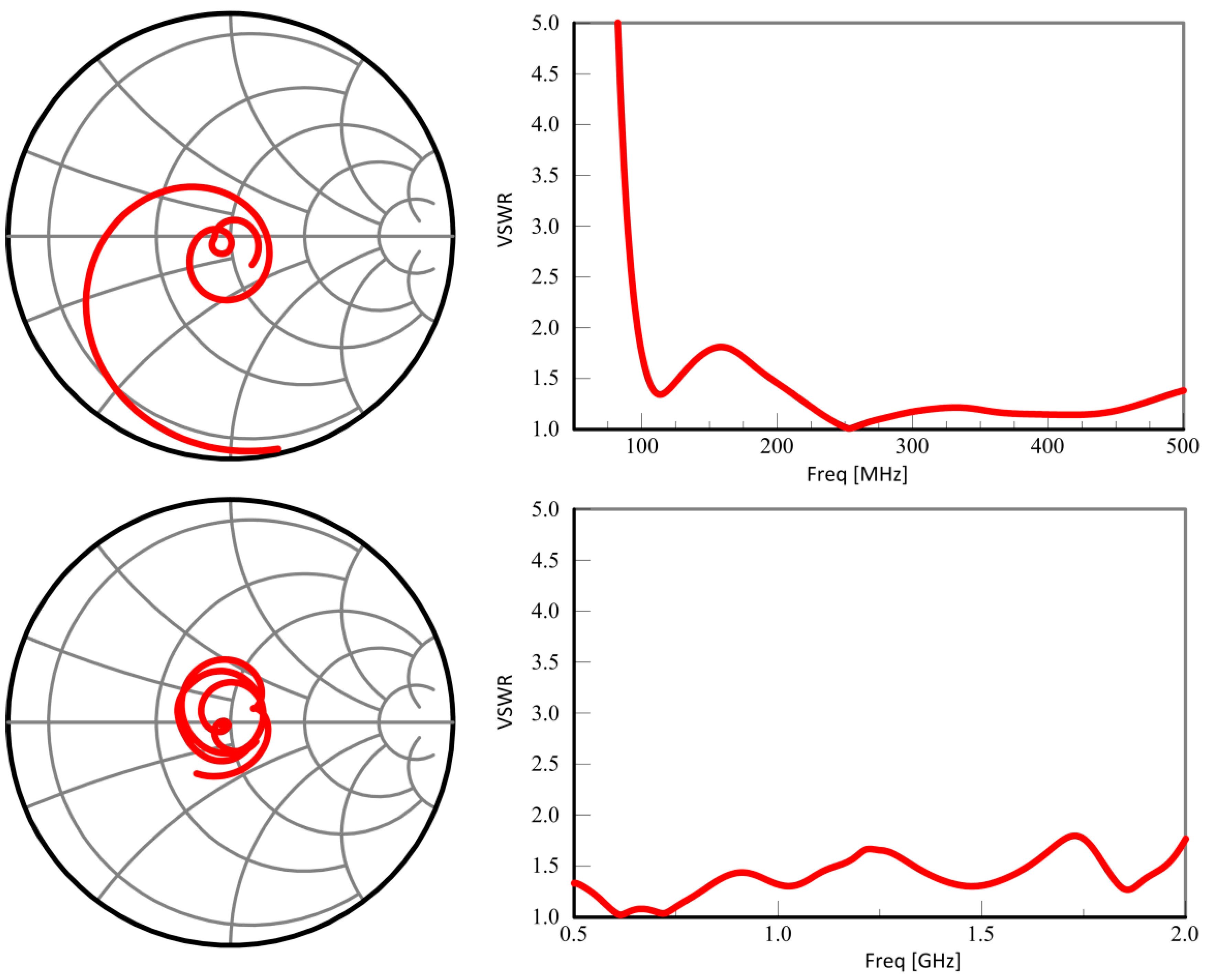
Figure 4 shows the simulated impedance results from 50 MHz to 2 GHz. The VSWR < 2.0 bandwidth occurs from 100 MHz to above 2 GHz.
Figure 4.
Impedance behavior of R2 = 12′′ case from 50 MHz to 2 GHz.
Figure 4.
Impedance behavior of R2 = 12′′ case from 50 MHz to 2 GHz.
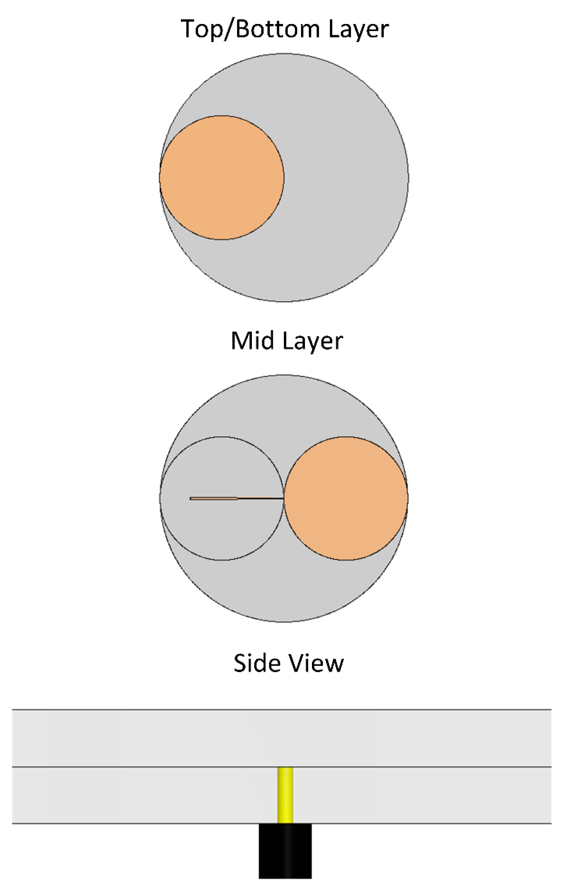
Next, a more realistic feed structure was developed. The metallization was divided into three layers to form a stripline feed as depicted below in
Figure 5. The advantages of utilizing a stripline feed are two-fold. First, the stripline feed, due to its balanced nature, reduces cross-polarization typically found in antipodal tapered antennas [
16]. Second, the groundplanes of the stripline serve as an electromagnetically shielded area to place the electronics, motors, sensors, and servos needed for flight. Two Rohacell sheets were introduced to facilitate this geometry. A 50 Ω coaxial feed was inserted through the bottom layer to excite the middle layer of a stripline. The stripline linearly tapers for a 50 to 75 Ω transition. The top and bottom metallizations serve as the groundplanes for the stripline feed.
The impedance behavior for the lower frequency region is similar to the previous lumped port model. However, the higher frequency region exhibits some spiking behavior at various frequencies where the match becomes worse. One possible explanation for this could be a backward propagating mode from where the coaxial feed comes into contact with the stripline central conductor. With this in mind, vias were introduced around this area to suppress this mode as shown in
Figure 6.
Figure 5.
Modified stripline feed design.
Figure 5.
Modified stripline feed design.
Figure 6.
Via placement in HFSS model.
Figure 6.
Via placement in HFSS model.
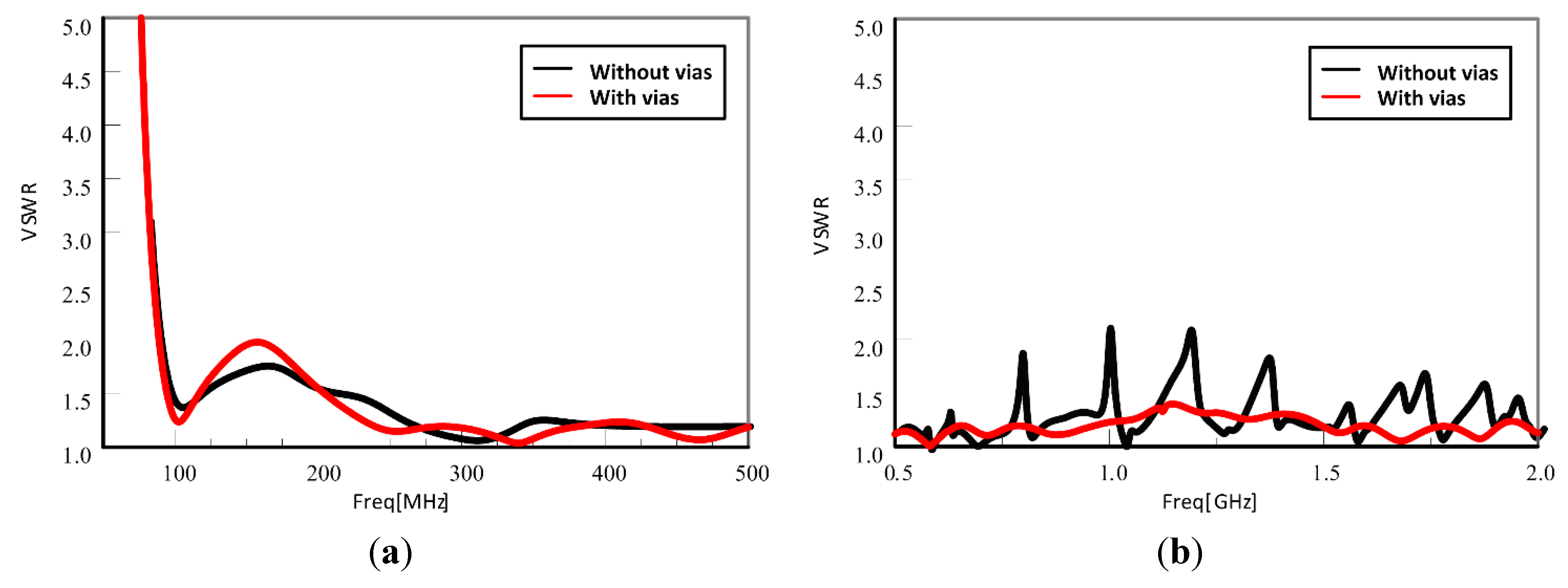
Figure 7 compares the impedance behavior without (black curve) and with (red curve) the proposed via shield. The peaking behavior in the larger frequency region is vastly improved and the antenna is matched from 100 MHz to over 2 GHz. Now, a physically realizable design has been developed which meets the desired antenna characteristics listed above.
Figure 7.
Impedance behavior of stripline-fed design without (black) and with (right) vias. (a) Low frequency sweep from 50 to 500 MHz; (b) Higher frequency sweep from 500 MHz to 2 GHz.
Figure 7.
Impedance behavior of stripline-fed design without (black) and with (right) vias. (a) Low frequency sweep from 50 to 500 MHz; (b) Higher frequency sweep from 500 MHz to 2 GHz.
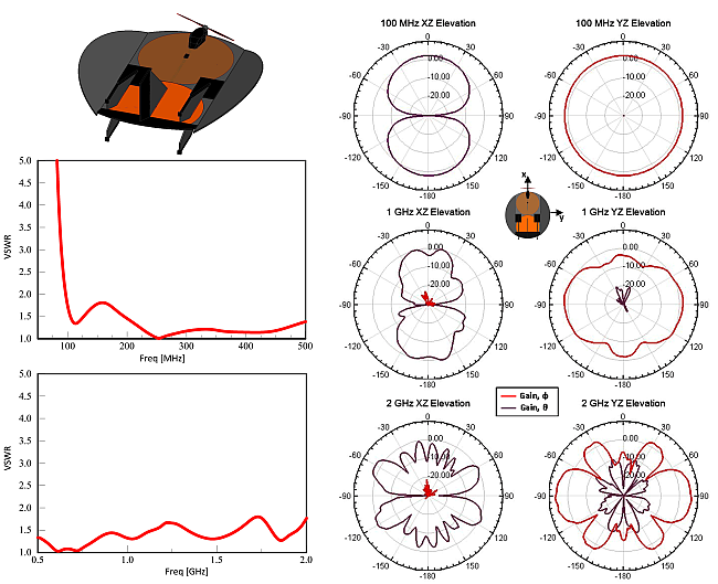
3. Aerodynamic Functionalization
The next stage of the design process involved modifying the antenna substrate into a lifting body. The lifting body chosen was based upon the Nutball flier. This RC hobbyist architecture consists of a flat, circular sheet of foam with a vertical tail in the aft section and positive dihedral for the wing tips to increase roll stability [
17]. The control surfaces include an elevator and a rudder for pitch and yaw/roll control, respectively. Many different size Nutball fliers have been developed in the hobbyist community from as small as 17′′ diameter to upwards of 42′′ diameter. The Nutball main flight mode is large angle of attack, slow moving cruise.
Preliminary flight testing was conducted on scaled models with 36′′ and 42′′ diameters. Untethered outdoor and tethered indoor flight tests were utilized for flight characteristic analysis. Flight tests showed large angle of attack, slow moving cruise as expected for this type of flier. Additional vertical fins were included to add vertical takeoff capability. Tethered indoor test system was primarily utilized for testing vertical takeoff capabilities. Improvement in vertical takeoff remains an ongoing process.
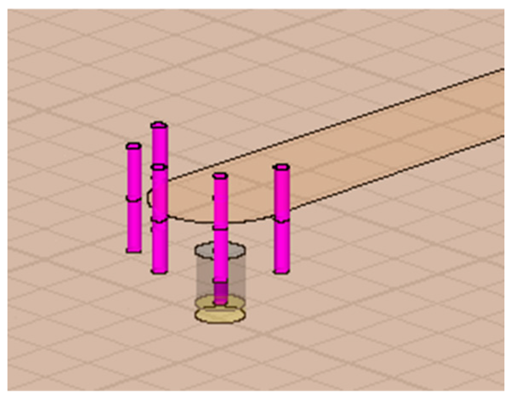
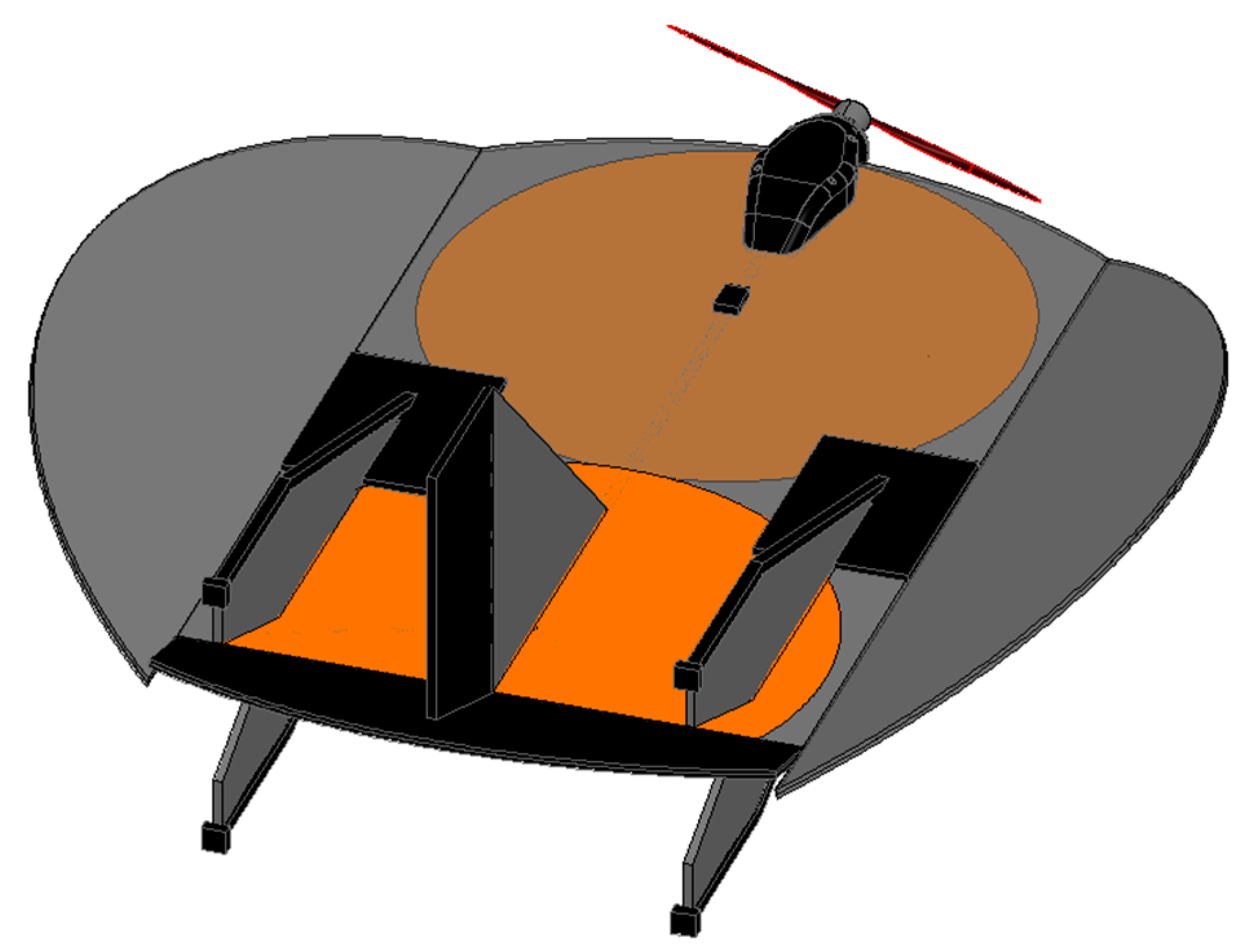
A new electromagnetic model was then created which included the aerodynamic structures as shown below in
Figure 8. All the electronics have been placed atop the groundplanes of the stripline feed to reduce electromagnetic interference to the antenna. These electronics include the motor, electronic speed controller, and receiver for flight control. The servos had to be placed outside this shielded area and were modeled as metallic cubes.
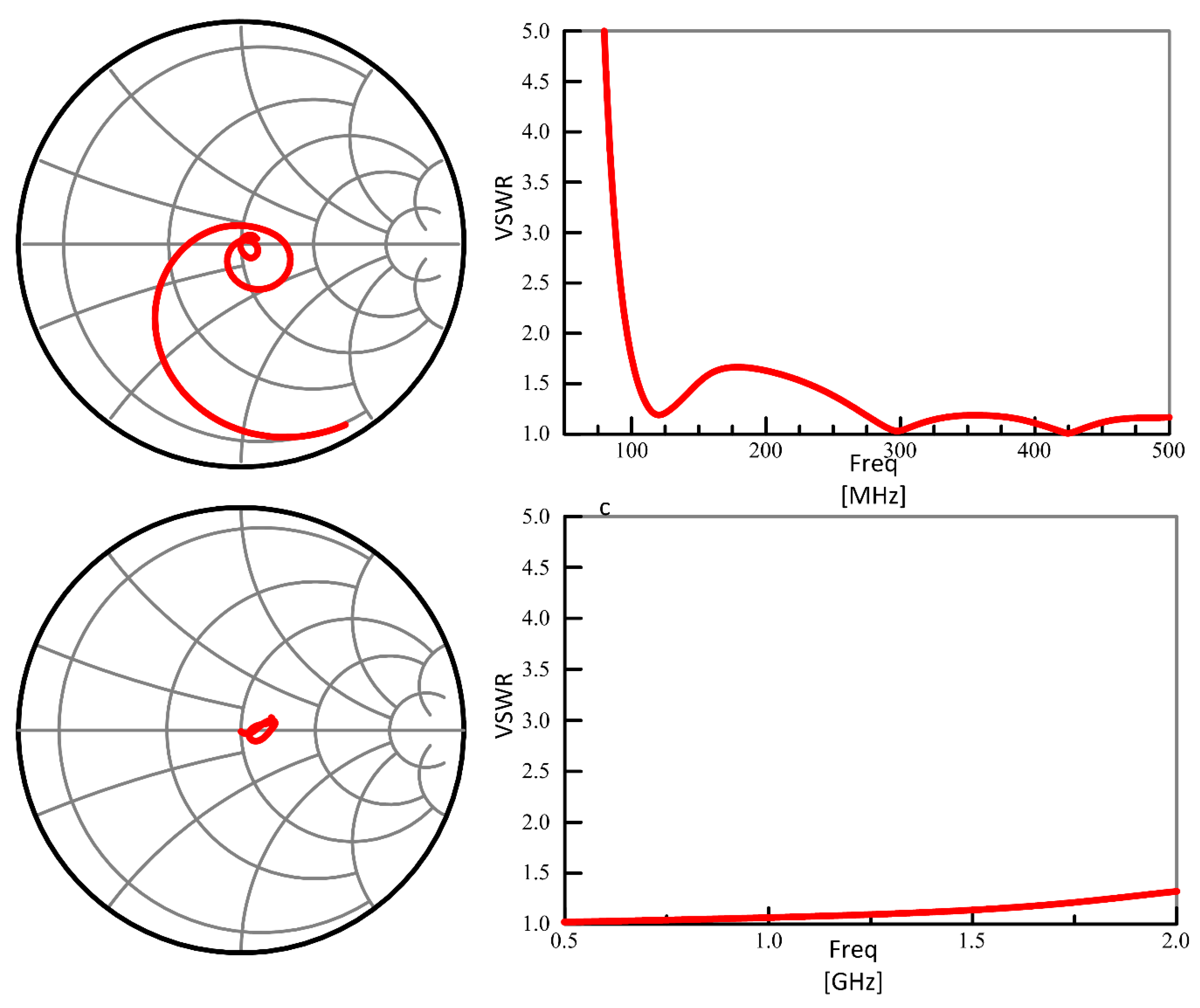
Figure 9 displays the resulting impedance behavior. Some detuning occurs over the band, but the VSWR still remains below 2 throughout the simulated bandwidth. Note that a cutout from the two rearward metallizations was implemented to avoid bending of the conductors as the elevator deflects.
Figure 8.
Complete electromagnetic model.
Figure 8.
Complete electromagnetic model.
Figure 9.
Impedance behavior for complete model.
Figure 9.
Impedance behavior for complete model.
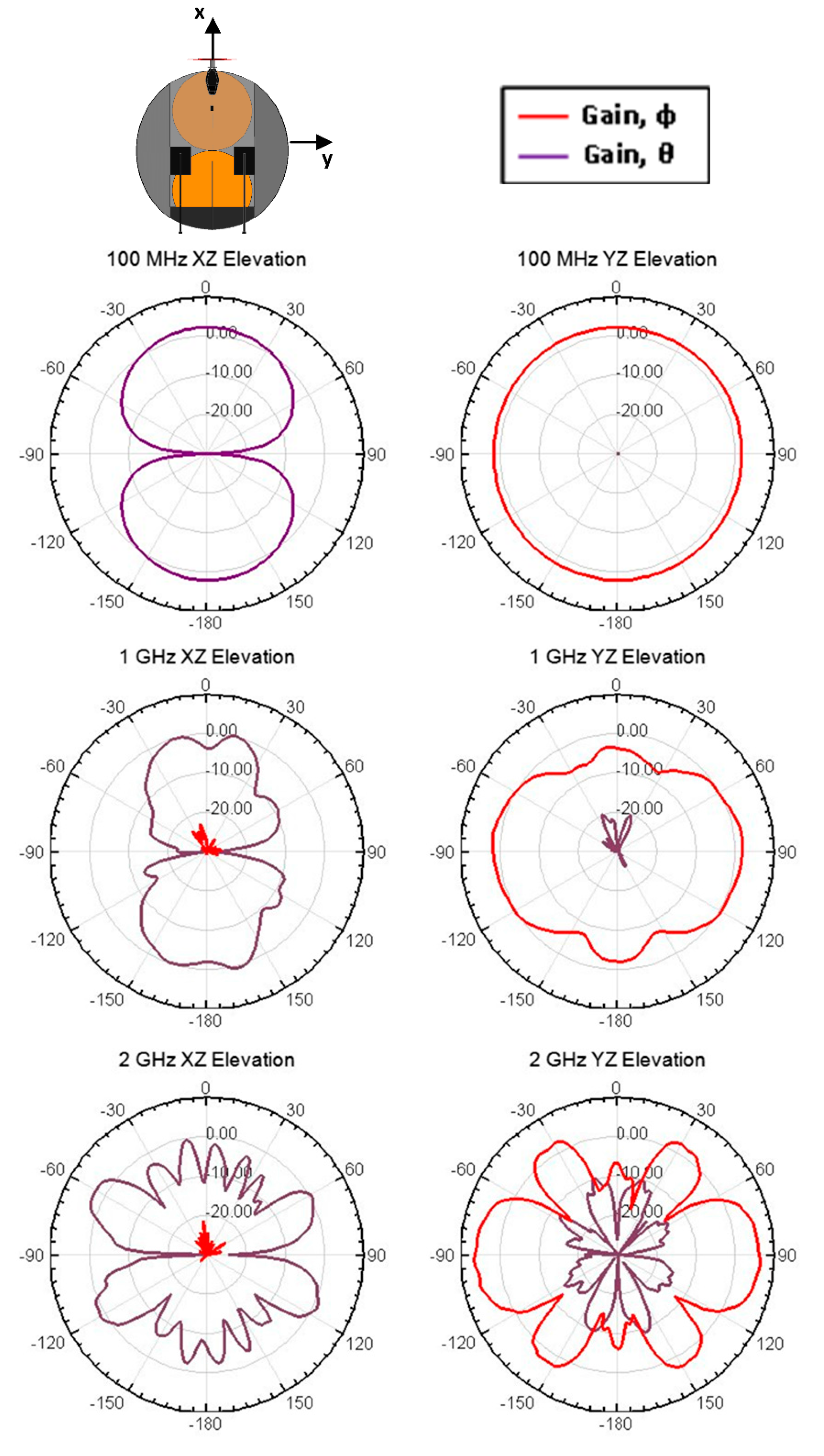
Next, the radiation patterns were analyzed.
Figure 10 shows the elevation radiation patterns for frequencies of 100 MHz, 1 GHz, and 2 GHz. The theta-polarized gain in the XZ plane exhibits a strong dipole-like mode at the lowest simulated frequency of 100 MHz. As the frequency increases, this theta-polarized gain displays more radiation lobes. The phi-polarized gain in the YZ plane exhibits stronger endfire behavior at frequencies above 100 MHz. This endfire behavior becomes more pronounced as the frequency increases to 2 GHz and is expected as the antenna transitions from the lowest order dipole mode to a higher frequency traveling wave mode.
Figure 10.
Radiation patterns for complete model.
Figure 10.
Radiation patterns for complete model.
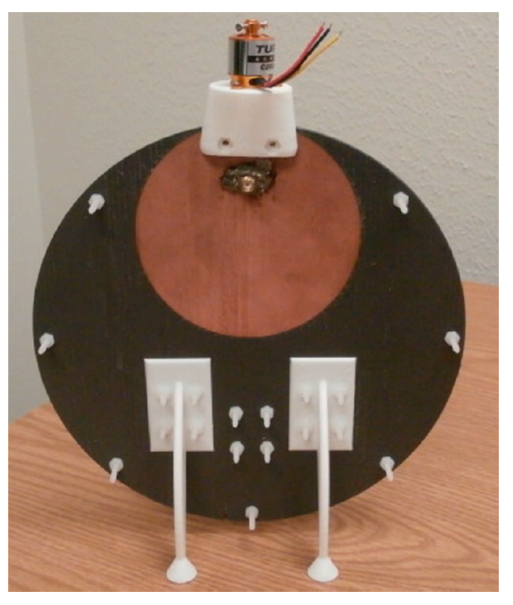
Finally, a scaled version of the proposed antenna geometry was fabricated with a diameter of 8′′ and a substrate of Rogers Duroid 5870 (see
Figure 11). Duroid was chosen as a readily available material which can be easily milled using conventional circuit milling technology with low electromagnetic losses. Two Duroid sheets for the required two antenna layers were joined by nylon screws as to minimize the electromagnetic interference created by standard metallic bindings. Flight stand, motor mount, and rudder (not shown) were fabricated using a 3D printer. A coaxial SMA connector formed the feed structure to the central stripline transmission line between the layers. One major difference between this fabricated structure and the simulated design is the lack of vias in the fabricated structure. The vias will be added in later editions of the fabricated model.
Figure 11.
Fabricated scaled design on Rogers Duroid 5870.
Figure 11.
Fabricated scaled design on Rogers Duroid 5870.
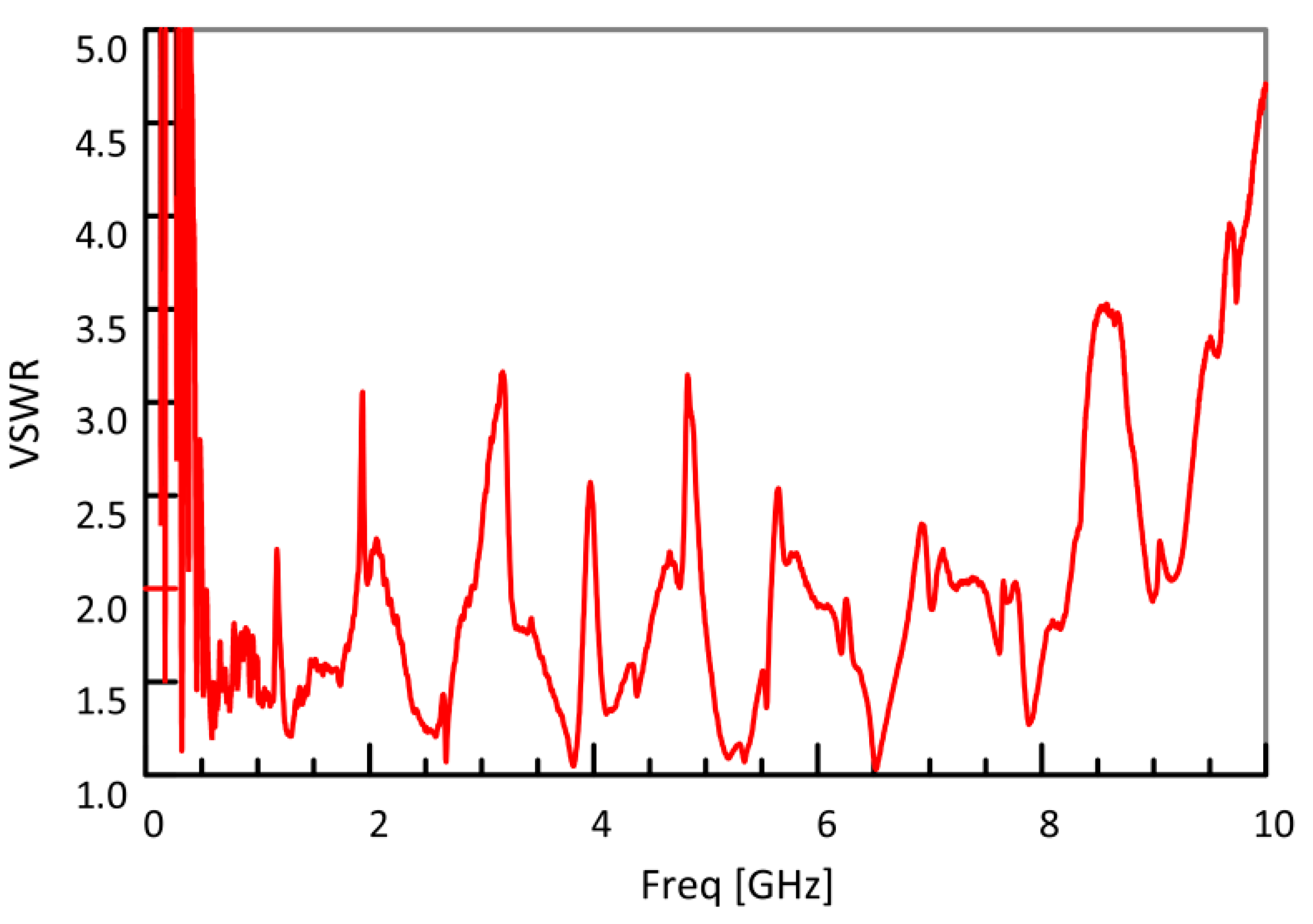
Figure 12 shows the measured impedance behavior for this fabricated prototype. The VSWR drops below 2 around 440 MHz and oscillates between values of 1.0 and 3.0 up to 8 GHz similar to the spikes found in the simulated model with no vias (see
Figure 7). It is expected that the addition of vias will improve this spiking behavior as shown in the simulations.
Figure 12.
Measured impedance behavior of scaled model.
Figure 12.
Measured impedance behavior of scaled model.
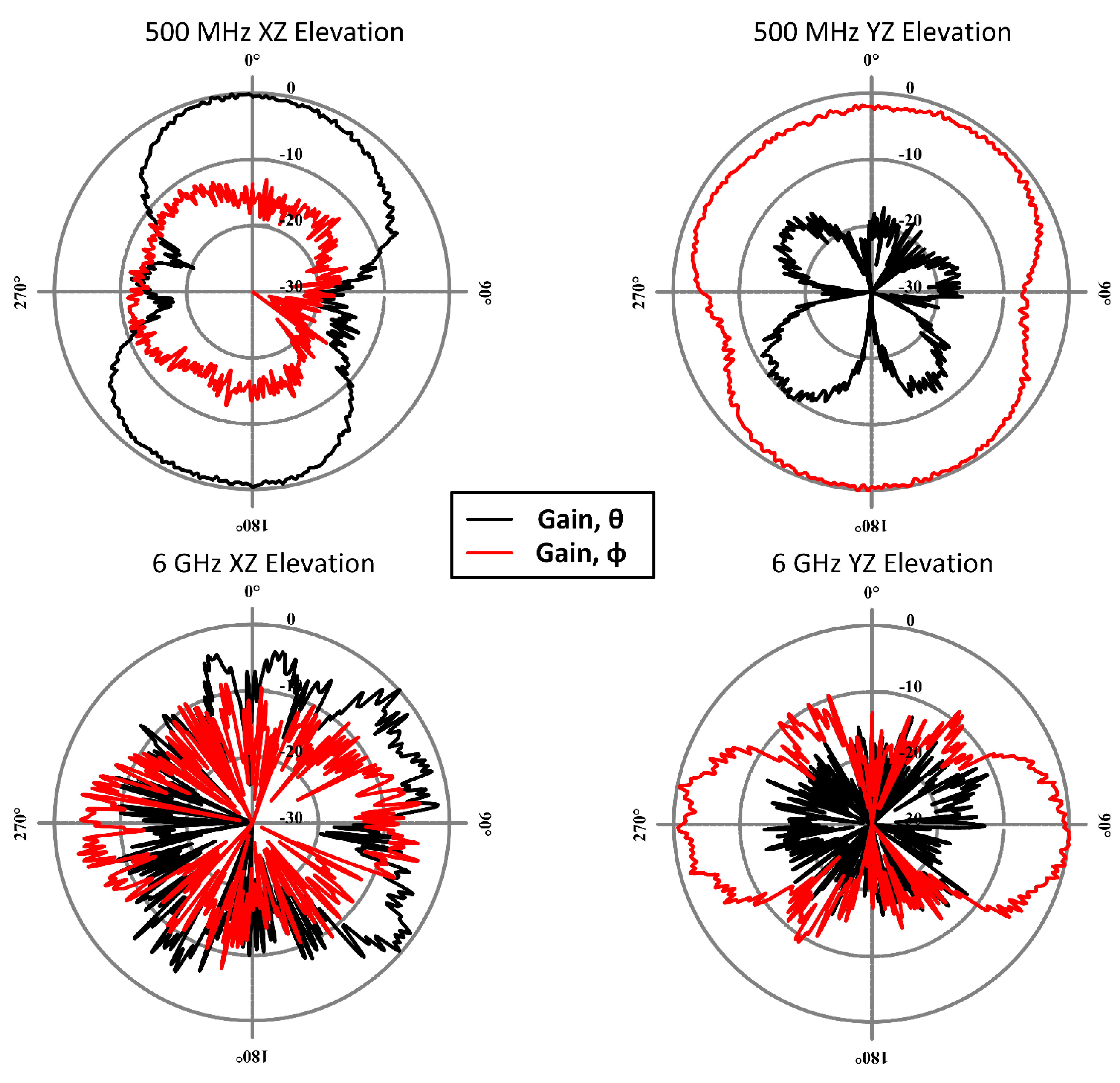
Figure 13 shows a sampling of the measured radiation characteristics for the prototype. Radiation testing was conducted over a frequency range from 500 MHz to 10 GHz. The results are similar to the simulated results shown in
Figure 12 with larger cross polarization and some distortion of the pattern. The fabricated model displays a dipole-like omnidirectional pattern at 500 MHz. The pattern becomes more pointed towards the direction of the slot in an end-fire mode as the frequency increases to 6 GHz similar to the larger model’s simulated behavior at 2 GHz.
Figure 13.
Radiation characteristics of scaled model.
Figure 13.
Radiation characteristics of scaled model.


