1. Introduction
Resistive sensors are widely used in various applications, including gas detection, humidity monitoring, temperature sensing, and biosignal acquisition. Among these, chemiresistive gas sensors—such as metal-oxide semiconductor (MOS) and conductive polymer-based types—are particularly attractive due to their low cost, structural simplicity, and compatibility with compact, embedded systems [
1,
2]. These sensors alter their electrical resistance in response to interactions with target gas molecules and are commonly applied in environmental monitoring, industrial safety, air quality control, agriculture, and smart home technologies, where continuous, low-power, and real-time sensing is essential [
3,
4,
5]. A key characteristic of chemiresistive gas sensors is their wide dynamic resistance range, typically spanning from a few hundred ohms to several hundred kilohms, and sometimes up to the megohm range, depending on gas concentration, ambient conditions, and sensor material. This wide variation poses a challenge for accurate resistance measurement, particularly at high resistances.
One widely used method is the resistance-to-time (R-to-T) technique [
6,
7,
8], which directly interfaces with a microcontroller by incorporating the sensor into an
RC charging or discharging circuit. This approach is appealing due to its simplicity, low cost, and minimal component requirements. However, its effectiveness significantly diminishes at higher resistances, where the time constant
becomes excessively large, leading to long measurement durations and sluggish response. Additionally, R-to-T methods are susceptible to parasitic capacitance, leakage currents, and timing jitter, making them unsuitable for resistances above several tens of kilohms or into the hundreds of kilohms range. To improve speed, a simplified time-to-digital readout architecture was proposed in [
9], achieving faster response; however, experimental validation was limited to resistances up to approximately 25 kΩ. An advanced R-to-T approach using a time-based, calibration-less readout was introduced in [
10], demonstrating high linearity (≤0.9%) and a wide sensing range from 10 kΩ to 10 GΩ using a CMOS-based implementation, though it required custom design and was primarily validated through simulation. Another widely used approach is resistance-to-frequency (R-to-F) conversion [
11,
12,
13], where variations in resistance are translated into shifts in oscillator frequency. This technique offers advantages such as fast response, wide dynamic range, and strong noise immunity. For instance, Qi et al. [
12] presented a CMOS interface achieving sub-ohm resolution across a 500 Ω to 10 MΩ range while maintaining high linearity and stable biasing. Yan et al. [
13] further enhanced this with a closed-loop architecture and PVT compensation, enabling rapid (1.7 μs settling time), low-power (98 μW) sensing across a 10 kΩ–100 MΩ range, making it suitable for dense sensor arrays. These R-to-F architectures are well-suited for integrated systems due to their compactness and energy efficiency, though they often require precise analog design and calibration to mitigate nonlinearity. To support wide-range resistive sensing, advanced CMOS and MEMS-based interfaces have also employed digitally programmable gain, transient analysis, and current-conveyor techniques to achieve high resolution without bulky passive components. However, these solutions tend to be complex and costly, limiting their accessibility in general-purpose or low-cost embedded applications.
Another common method is resistance-to-voltage (R-to-V) conversion, typically implemented using a voltage divider, where the output voltage is read by a microcontroller’s ADC [
4,
14,
15]. This method is valued for its simplicity, low cost, and fast response time, as it allows continuous analog measurements without requiring complex timing or frequency detection circuits. However, it suffers from nonlinear behavior when the sensor resistance becomes very low or very high. In such cases, the divided voltage approaches the supply rails, compressing the ADC’s input dynamic range and reducing measurement resolution and accuracy. To address this limitation, adaptive divider techniques using digital potentiometers have been proposed, allowing dynamic adjustment of the reference resistance to keep the output voltage near mid-scale. One such implementation achieved a maximum relative error of 0.88% across a 1 kΩ to 1 MΩ range using a 16-bit ADC [
16]. While effective, these techniques require high-resolution ADCs and programmable resistor arrays, which increase system cost and complexity, especially in multi-sensor applications.
Another popular solution is the multiple-interval approach [
17], as illustrated in
Figure 1, where the sensor is excited with a fixed voltage and the current flows through a selectable resistor based on the estimated range, followed by a programmable gain amplifier (PGA) for output scaling. While effective, this technique requires accurate component matching, gain calibration, and complex timing control. Additionally, in multi-sensor systems, placing the sensor in series with the excitation source complicates analog switching and may require duplicated analog front-ends or additional circuitry, increasing cost and design overhead.
To address these challenges, this paper proposes a microcontroller-based measurement system that employs an adaptive constant current source using an inverting amplifier with a fixed reference resistor and a PWM-controlled reference voltage. This configuration allows linear R-to-V conversion and ensures the output remains within the ADC’s optimal range, even as resistance varies over multiple decades. The digitally controlled current allows real-time adaptation without high-resolution DACs or PGAs. Furthermore, the system is particularly suited for multi-sensor platforms such as electronic noses [
18,
19,
20], which commonly utilize MQ and TGS gas sensors. These sensors typically exhibit resistance ranges between 1 kΩ and 100 kΩ, as shown in [
21]. By supporting sensor selection via analog switches, the proposed design eliminates the need for replicated analog front-end circuits, resulting in a compact, cost-effective, and scalable solution for embedded applications.
The structure of this paper is organized as follows:
Section 2 presents the proposed system architecture, including the circuit configuration, principle of operation, measurement algorithm, and error analysis.
Section 3 provides the experimental results validating the system’s performance.
Section 4 offers a detailed discussion of the results and the implications of the proposed method. Finally,
Section 5 concludes this paper with a summary of key findings and insights into the applicability of the approach.
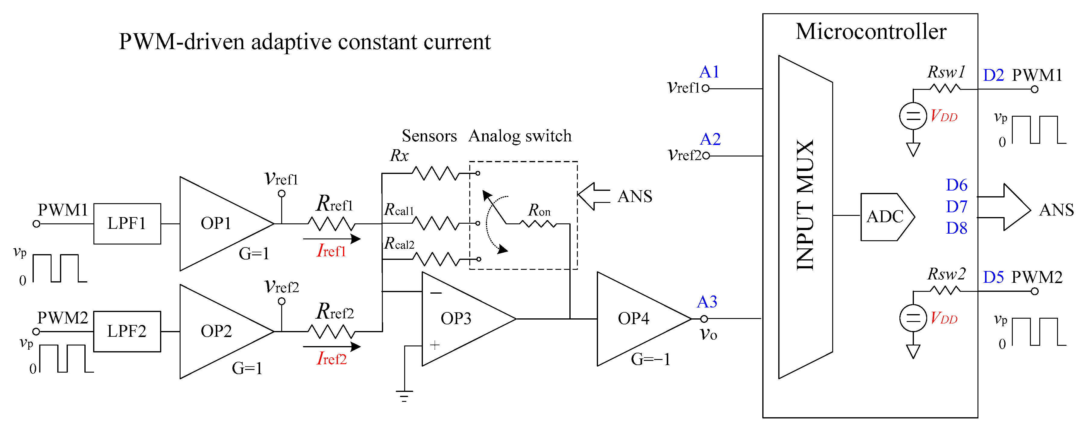
2. Proposed Measurement System
To overcome the limitations of traditional methods in handling wide sensor resistance variations, this paper presents a digitally controlled, multiple-interval measurement system based on PWM-driven adaptive current sources. The design enables accurate and scalable multi-sensor support with automated calibration and current range adjustment. The principle of operation, design methodology, and associated error considerations are detailed in the following subsections.
2.1. Principle Operation
Figure 2 illustrates the proposed system architecture for accurately measuring resistive sensors over a wide dynamic range using an adaptive constant current source driven by a PWM signal. The system is composed of three primary functional blocks: the PWM-to-voltage conversion stage, the programmable current generation stage, and the sensor measurement and acquisition stage. A high-frequency PWM signal is generated by the microcontroller and passed through a low-pass
RC filter to produce a smoothed DC voltage. This voltage generates a current source that excites the resistive sensor. In its simplest form, a single PWM channel can provide adaptive current control over a moderate resistance range. However, when a wider range of sensor resistances must be measured, this approach becomes limited by the constrained voltage range that can be generated by the PWM source (typically between 1 V and 5 V). At very low PWM duty cycles, the filtered voltage becomes too small to generate a measurable output across low-resistance sensors, while at high duty cycles, the voltage may approach the op-amp’s supply rail or ADC saturation. To overcome this limitation, the system incorporates multiple independently controlled PWM channels, each generating a different excitation level. The microcontroller selects or combines the appropriate PWM channels based on the sensor’s resistance range to ensure that the output voltage remains within the ADC’s high-resolution window, allowing accurate measurement over several decades of resistance.
In the second stage, a multi-level constant current source is implemented using an inverting amplifier configuration. For each channel n, the excitation current is defined by , where is the filtered voltage from the n-th PWM signal and is the corresponding reference resistor. These currents are selectively applied to the sensor under test through an analog switch. By choosing the appropriate PWM-controlled current path based on the sensor’s resistance range, the system ensures that the resulting output voltage remains within the ADC’s optimal input range, enabling accurate and efficient resistance measurement.
For the sensor measurement and acquisition stage, the sensor resistance
can initially be calculated using the following direct equation:
where
is the known reference resistor used in the current path, and
,
are the measured reference and output voltages, respectively. However, this basic approach may suffer from errors due to variations in the PWM-generated voltage, op-amp offset, and component tolerances.
To improve accuracy, a calibration-based compensation method is employed. In this process, a known calibration resistor
is connected under the same configuration to acquire reference voltages
and
during calibration. These are then used alongside measurement voltages to compute the unknown resistance as follows:
This method effectively compensates for gain variations, reference voltage deviations, op-amp offset and other linear drifts between the calibration and measurement phases. Equation (2) assumes that the internal on-resistance of the analog switch (
) is negligible. However, in practice,
may vary with supply voltage, temperature, and the active channel [
22], potentially introducing significant error—especially when
is small. To address this, Equation (2) can be extended to the following Equation (3):
2.2. Component Selection
This section outlines the design considerations and optimal component selection for the proposed measurement system. To ensure compatibility with the microcontroller’s ADC input range, the output voltage is constrained to remain within 1 V to 4.75 V. Additionally, to minimize nonlinearities and ripple in the filtered PWM signal, the PWM duty cycle is limited to a practical range between 0.2 and 0.95. These limits correspond to reference voltages ranging approximately from 1 V to 4.75 V. Under these constraints, the excitation current is adjusted by selecting an appropriate reference resistor to maintain within the desired range across the full span of sensor resistances.
2.2.1. Optimal Reference Resistance
The minimum and maximum required excitation currents are determined based on the target output voltage limits and the sensor resistance range, as follows:
Once the desired current range is known, the reference resistor
can be calculated using the average reference voltage and the midpoint of the excitation current range.
This method ensures that the selected reference resistor provides effective control over the excitation current across the target resistance range, while keeping within the ADC’s optimal resolution window.
2.2.2. Calibrated Resistance
The calibration resistor
is selected to be equal to the minimum expected sensor resistance
. This choice is critical for accurately estimating the internal resistance of the analog switch
, which typically ranges from 125 Ω to 240 Ω at 25 °C when operated with V
DD = 15 V, depending on the specific device and operating conditions [
22]. Using a low-value calibration resistor (e.g., 1 kΩ) amplifies the effect of
on the measured result, thereby improving the sensitivity and accuracy of the resistance estimation. In contrast, if a higher-value
were used, the relative influence of
would diminish, making it more difficult to isolate and compensate for this error source. This initial calibration step is essential for mitigating switching resistance effects, particularly in low-resistance measurements, and is seamlessly integrated into the system’s adaptive correction algorithm.
2.2.3. RC Filter
To generate a stable analog voltage from the PWM signal, a low-pass RC filter is applied to remove high-frequency switching components and produce a smooth DC level. The filter cutoff frequency is selected to be significantly lower than the PWM switching frequency to ensure an adequate attenuation of ripple, while maintaining a fast enough response for dynamic adjustment. In this work, a PWM frequency of approximately 31.25 kHz is used, and the filter time constant is chosen accordingly (e.g., R = 10 kΩ, C = 100 nF, yielding a cutoff frequency of approximately 160 Hz). This provides a good balance between ripple suppression and responsiveness, ensuring that the filtered reference voltage remains stable during measurement. Proper filtering is essential to maintain linearity in the excitation current and to avoid introducing noise or distortion into the sensor voltage measurement.
2.3. Algorithm Measurement Process
The PWM-controlled voltage source is employed to generate a programmable excitation current, which is adaptively tuned according to the estimated resistance range of the target sensor. In this study, two resistance intervals are considered: 1–10 kΩ and 10–100 kΩ. To support these ranges, two PWM channels are configured: PWM1 for the low-resistance range (1–10 kΩ) and PWM2 for the high-resistance range (10–100 kΩ).
Figure 3 illustrates the flowchart of the measurement algorithm used to determine the unknown resistance
using the proposed dual-PWM excitation system. The process begins by measuring the calibration parameters—
,
, and
—using a known calibration resistor
. Next, the system selects the appropriate PWM channel by temporarily setting PWM1 to a low duty cycle (e.g., 0.2). If the resulting output voltage
exceeds 4.75 V, indicating that the resistance is too high for PWM1, the system switches to PWM2. The actual sensor measurement then proceeds by setting an initial PWM duty cycle (e.g., 0.95), measuring
, and incrementally reducing the duty cycle to bring the output voltage within the desired range. The detailed steps are described in the following subsections.
2.3.1. Measurement
In the first step, the microcontroller controls the analog switch to connect a known calibration resistor
in place of the sensor. This step is used to estimate the internal resistance of the analog switch,
, for each measurement channel
n. A predefined reference resistor
is used, and the PWM duty cycle is set to a moderate value (e.g., 0.5–0.95) to produce a stable and measurable reference voltage
. The output voltage
is then measured, and the on-resistance is calculated using the following expression:
The values , along with and are stored in memory and used later for calculating the unknown sensor resistance using the compensation formula (Equation (3)).
2.3.2. Measurement
In the second step, the system measures the unknown sensor resistance . The microcontroller configures the analog switch to connect the target sensor in place of the calibration resistor. The measurement begins with PWM1, which is assigned to the low-resistance range (1–10 kΩ). The PWM duty cycle is initially set to a high value (e.g., D = 0.95) to generate a strong excitation current. The resulting output voltage is then measured.
If
, the resistance
is calculated using the compensation formula (Equation (3)). If
exceeds 4.75 V, the PWM duty cycle is gradually reduced (e.g., in steps of 0.05) until the output voltage falls within the desired range. If the duty cycle reaches its lower bound (e.g.,
D = 0.2) and
remains above 4.75 V, this indicates that the sensor resistance exceeds the measurable range of PWM1. In this case, the system switches to PWM2, which is configured for the high-resistance range (10–100 kΩ). The same process is repeated; the duty cycle is adjusted until the output voltage is within range, and then
is computed using the stored calibration values and Equation (3). Each ADC channel conversion takes approximately 120 µs to complete (p. 273, [
23]). During the calibration phase, two node voltages—
and
—are acquired with one ADC sample each, requiring about 240 µs. Similarly, two measurements are taken during the sensor reading phase. If the initial output exceeds 4.75 V, the system reduces the PWM duty cycle step-by-step, with each iteration consuming ~250 µs. In the worst-case scenario (17 steps), this results in a maximum adjustment time of ~4.25 ms. Including calibration, the total worst-case process time is approximately 4.50 ms. To improve measurement accuracy and reduce the impact of ADC quantization noise, averaging multiple ADC samples is recommended. For example, using 100 samples per voltage point increases the total processing time to approximately 450 ms, which remains acceptable for real-time monitoring in gas sensing applications using MQ and TGS sensor families.
To ensure accurate excitation current during measurement, it is important to isolate inactive PWM channels. Each PWM output drives an RC filter, and the residual impedance of an unused filter may interfere with the summing node of the inverting amplifier. To prevent such effects, the inactive PWM pin is reconfigured as a digital input during the measurement cycle. For example, when PWM1 is selected, PWM2 is set to high-impedance input mode, and vice versa. This prevents leakage paths and ensures that only the active PWM channel contributes to the excitation current , thereby maintaining stable and accurate sensor readings.
2.3.3. Multiple Sensor Measurement
The proposed system can be extended to support multiple resistive sensors by incorporating a microcontroller-controlled analog switch. The microcontroller sequentially activates each switch channel to connect one sensor at a time to the measurement circuit. Once a specific sensor is connected, the measurement process proceeds using the same two-step algorithm described in
Section 2.3.1 and
Section 2.3.2—first estimating the internal switch resistance
using a calibration resistor (if required), followed by adaptive PWM-based measurement of the unknown resistance
.
This sequential measurement strategy allows multiple sensors to share a common analog front-end, significantly reducing circuit complexity and cost. Since only one sensor is actively measured at a time, interference between channels is minimized. The system stores the calibration values
,
and
for each channel, enabling accurate compensation for each individual measurement without requiring repeated calibration during normal operation. This enhances both accuracy and measurement speed across multiple sensors. Overall, this configuration offers a scalable solution for multi-sensor platforms—such as electronic nose arrays [
18,
19,
20]—without the need for duplicated analog components or complex multiplexing circuits. It is particularly well-suited for applications where cost, board space, and power efficiency are critical design constraints.
2.4. Error Analysis
Although the proposed system offers a compact and flexible method for wide-range resistive sensor measurement, several sources of error can affect the overall accuracy. These include errors introduced by the RC filter circuit, op-amp limitations, ADC quantization and nonlinearity, analog switch resistance, and PWM ripple. Each of these factors is discussed below.
2.4.1. RC Filter and PWM Ripple
The PWM-to-analog voltage conversion depends on a low-pass RC filter to smooth the digital PWM waveform into a stable voltage. If the cutoff frequency of the filter is too close to the PWM frequency, or if the filter time constant is too short, residual ripple may appear on the filtered voltage. This ripple introduces excitation current fluctuations and causes to vary slightly during ADC sampling, leading to measurement instability and reduced accuracy. To reduce the effects of PWM ripple and ensure stable analog voltage generation, two key measures are implemented. First, a high-frequency PWM signal at 31.25 kHz is used, allowing effective low-pass filtering with a practical RC time constant. The filter’s cutoff frequency is selected to be at least one to two decades below the PWM frequency—for example, using R = 10 kΩ and C = 100 nF yields a cutoff around 160 Hz, which provides strong attenuation of the PWM switching components. Second, to prevent instability and poor filtering performance near the extremes of the PWM range, the duty cycle is limited to a practical range between 0.2 and 0.95, ensuring that the filtered voltage remains within a controllable and linear region.
2.4.2. Op-Amp Offset
Operational amplifiers typically exhibit a small input offset voltage, which can result in a shift in the output voltage even when the differential input is ideally zero. In resistive measurement systems, this offset can propagate through the excitation current path and directly affect the measured output voltage , particularly when the excitation current is low or the sensor resistance is small. This introduces a fixed error in the calculated sensor resistance. In the proposed system, the influence of op-amp offset is significantly reduced through the use of a calibration-based compensation method. By measuring a known calibration resistor under the same configuration as the unknown sensor, the offset is embedded equally in both the calibration and measurement stages. When computing the resistance using the ratio-based formula, the offset contributions largely cancel out, minimizing their impact on accuracy. This approach provides robust offset compensation without requiring ultra-low-offset op-amps.
However, for measurements involving very high resistances (e.g., above 100 kΩ), the offset voltage, along with the op-amp’s input bias current, becomes more critical. These factors, combined with leakage current from analog switches and increased susceptibility to noise, may limit the system’s performance in the megaohm range. Addressing these limitations would require the use of precision op-amps with ultra-low input bias current, along with additional circuit techniques such as guard rings or shielded layouts, which may increase system complexity and cost.
2.4.3. Analog Switch Resistance
The internal resistance of the analog switch introduces a series resistance error, particularly in the low-resistance measurement range. According to the datasheet,
typically ranges from 125 Ω to 240 Ω at 25 °C when operated at V
DD = 15 V, and it can vary with supply voltage, input signal level, temperature, and the selected channel. Therefore, it must be estimated and compensated through calibration. This is most critical when measuring resistances near 1 kΩ, where an uncompensated
can lead to several percent error. In the proposed system,
is approximated during the calibration process using a known reference resistor
, connected through one channel of the analog switch. However, because
varies between channels, compensation based on a single channel may not be fully accurate for others. According to datasheet specifications, this variation can be in the range of 5–15 Ω between channels [
22]. While this is negligible for high-resistance measurements, it should be taken into account when high accuracy is required in the low-resistance range.
2.4.4. Calibration Resistance
While the reference resistor defines the excitation current , it is not directly involved in the final computation of the unknown resistance . Instead, the accuracy of the measurement primarily depends on the calibration resistor , which is used as a known reference in the compensated ratio calculation. Any deviation between the nominal and actual value of introduces a proportional error in the result. To minimize this source of error, the actual resistance of is measured using a calibrated digital ohmmeter, and this measured value is used in all resistance calculations. This approach effectively eliminates the impact of resistor tolerance and ensures higher accuracy in the measurement process.
2.4.5. Microcontroller ADC
During each measurement cycle, the system samples four node voltages:
,
,
and
. Although
and
as well as
and
are measured at the same physical nodes, they are recorded at different times—before and after switching from the calibration resistor
to the unknown sensor
. These voltages are digitized by the microcontroller’s ADC, which is typically affected by gain and offset errors. The digitized output can be modeled as follows [
24]:
where:
: measured voltage (in volts) from the ADC,
: raw digital code output from the ADC corresponding to the analog voltage,
: ADC reference voltage (typically the supply voltage),
N: ADC resolution, equal to 2m, where m is the number of bits (e.g., N = 1024 for a 10-bit ADC),
: ADC gain error (unitless), representing scale deviation from ideal conversion,
: ADC offset error in digital code units.
By substituting this ADC model into the compensated resistance Equation (3), the measured resistance
becomes the following:
This formulation shows how the ADC’s gain error β and offset error affect the calculated resistance. Since the gain error term appears symmetrically in both the numerator and denominator of each ratio, its influence largely cancels out. However, the offset error does not fully cancel—particularly when the digital outputs are small and comparable in magnitude to . Nevertheless, when , the relative contribution of the offset becomes negligible. This confirms that the proposed compensation method—based on the ratio of measured voltages—effectively suppresses the impact of both gain and offset errors, making the technique robust even with low-resolution or imperfect ADCs.
3. Experimental Results
The experimental setup was implemented using an Arduino Mega2560 microcontroller (distributed by P-BOT, Bangkok, Thailand; manufactured in China), which features a 10-bit ADC and was powered by a measured of 5.01 V. The analog front-end, including op-amps and the analog switch, was powered by a ±6 V dual supply. The circuit utilized four OP07 op-amps: two for buffering the PWM-filtered voltages and two for the inverting amplifier and output buffer stages. The PWM output was filtered using an RC low-pass filter with kΩ and , yielding a cutoff frequency of approximately 160 Hz, which provides effective ripple suppression at the PWM switching frequency of 31.25 kHz. Two fixed reference resistors were used to generate excitation currents: Ω for the 1–10 kΩ range and Ω for the 10–100 kΩ range. A CD4051B analog switch, also powered by ±6 V, was used to select between calibration resistors and sensors. Calibration was performed using Ω and Ω, and test resistors spanning from 1 kΩ to 100 kΩ were used to validate performance. All resistor values, including , , and , were measured using a TECPEL DMM8050 digital multimeter for accurate reference comparison.
3.1. Evaluation of Measurement Accuracy
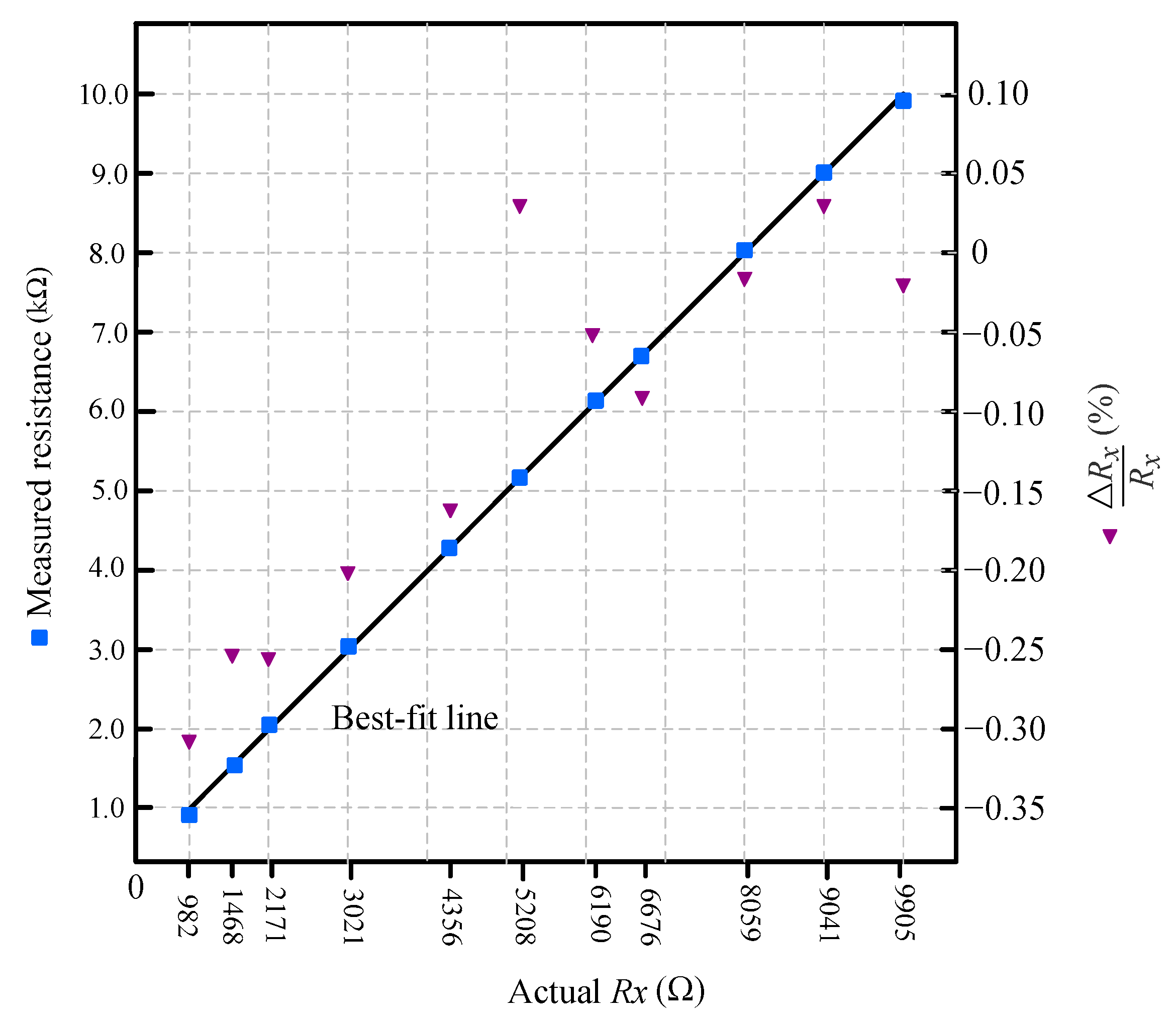
For the initial validation, the system was tested without the analog switch to directly examine the accuracy and intrinsic error of the measurement circuit. In this test, the unknown resistance was calculated using the simplified Equation (1), which avoids potential error sources such as analog switch resistance or calibration mismatches. This approach evaluates the core performance of the system—specifically the PWM-filtered voltage source, op-amp stability, and ADC resolution.
Figure 4 shows the measured resistance values plotted against actual
, along with the Relative Error,
(%) plotted on the secondary axis. Each data point was obtained by averaging 100 ADC samples to reduce noise. The best-fit line demonstrates strong linearity across the tested range from approximately 1 kΩ to 10 kΩ. The relative error remains within ±0.31%, indicating high accuracy of the system even without full calibration.
In addition to the low-resistance range, the system was also evaluated in the high-resistance range from 10 kΩ to 100 kΩ using the same simplified measurement method (Equation (1)), without analog switching or calibration. The results are shown in
Figure 5, where the measured resistance is plotted against the actual value, and the relative error
(%) is displayed on the secondary axis. Each point represents an average of 100 ADC samples to minimize noise.
While the system maintains good linearity across the entire range, the relative error in this region is slightly higher compared to the 1–10 kΩ range, reaching up to approximately ±0.35%. This increased error is attributed to the reduced excitation current at higher resistances, which results in smaller output voltages and increased sensitivity to op-amp offset, ADC resolution, and ripple in the PWM-filtered reference. Nonetheless, the measurement accuracy remains within acceptable limits, validating the effectiveness of the base system over a broader dynamic range.
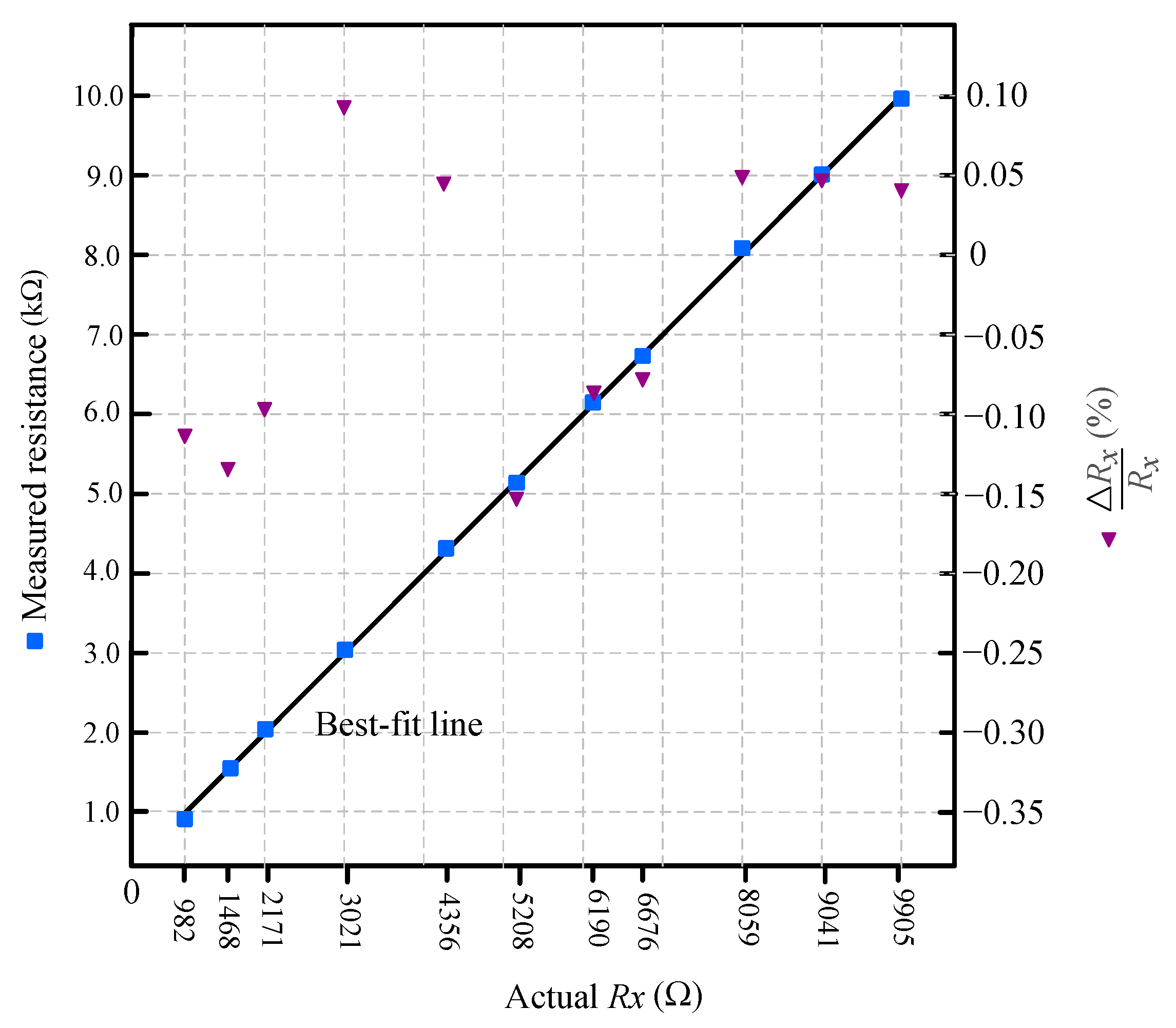
3.2. Accuracy Verification with Full Measurement Procedure
Figure 6 shows the calibrated measurement results for the 1–10 kΩ resistance range using the full procedure described in
Section 2.3. In this test, the system first connected a known calibration resistor (
Ω) and applied a PWM duty cycle of 0.9 to generate the reference voltage. The measured values were
and
, which were used to calculate the analog switch resistance
using Equation (7).
The system then sequentially connected each unknown resistor , starting with a PWM duty cycle of 0.95. If the resulting exceeded 4.75 V, the duty cycle was reduced in 0.05 steps (e.g., 0.90, 0.85, etc.) until entered the valid ADC input range.
Each resistance value was calculated using the compensated method in Equation (3), with 100 ADC samples averaged per point to reduce noise. The plot demonstrates a strong linear correlation between the measured and actual resistances. Relative errors remained within ±0.15%, confirming the effectiveness of the proposed calibration approach in improving accuracy over the low-resistance range while compensating for switch resistance and system offsets. Compared to the simplified method using Equation (1), the compensated technique in Equation (3) showed improved accuracy, with a maximum relative error of approximately 0.15%, lower than the uncalibrated case. This improvement is primarily due to the effective cancellation of op-amp offset voltage, which is a dominant source of error in low-voltage analog measurements. Since the same op-amp offset affects both the calibration and measurement voltages, the ratio-based structure of Equation (3) significantly suppresses its impact. This makes the proposed method robust against internal analog errors without requiring precision or zero-drift op-amps.
Figure 7 shows the measurement results for the 10–100 k
range using the full calibration-based technique described in
Section 2.3, with automatic PWM channel switching. The system initially attempted measurement using PWM1, which was designed for low-resistance excitation. When PWM1 was set to a duty cycle of
D = 0.2 (minimum allowed), the resulting
still exceeded 4.75 V, indicating that the resistance exceeded the measurable range for PWM1. In response, PWM1 was disabled (configured as a digital input), and PWM2—configured for high-resistance excitation—was activated. Due to the fixed reference resistor
Ω, the minimum excitation current from PWM1 is approximately 303 µA, which limits its maximum measurable resistance to
kΩ. Consequently, there is an overlapping or intersection region between the operational ranges of PWM1 and PWM2, approximately in the 10–20 kΩ span. This overlap ensures a smooth transition and avoids blind zones in resistance measurement across the two ranges. The calibration for PWM2 was performed using
Ω, with
and
, resulting in a calculated
Ω and stored for subsequent compensation. The system then proceeded to measure each unknown
by checking
and adjusting the PWM2 duty cycle in 0.05 steps to bring
into the 1–4.75 V range before computing
using Equation (3).
The measured values in
Figure 7 exhibit good linearity, with a maximum relative error of approximately ±0.33%. This error is slightly higher than in the 1–10 kΩ range, primarily due to lower excitation currents and increased sensitivity to op-amp offset voltage and ADC quantization effects at higher resistances. When compared to the uncompensated results in
Figure 5, the error levels appear similar; however, it is important to note that the experimental conditions—such as offset voltage and reference stability—were not varied between the two tests. Therefore, the full advantage of the compensation method may not be fully reflected in this comparison. Nonetheless, the results confirm that the proposed calibration and PWM-switching strategy effectively extends the measurable resistance range while maintaining acceptable accuracy.
To evaluate the system’s short-term repeatability and noise robustness, 100 consecutive readings were collected for a fixed resistor with a nominal value of 982 Ω. Each reading was computed as the average of 100 ADC samples, consistent with the method used throughout this study. As shown in
Figure 8, the histogram reveals that most results cluster tightly around 981 Ω, indicating stable and consistent measurements. This resistor value is close to the calibration resistor
Ω, which minimizes the impact of nonlinearity and residual calibration errors, further enhancing accuracy. The standard deviation (σ) was calculated to be 0.818 Ω, the repeatability error (
eR) was 0.083%, and the signal-to-noise ratio (SNR) was 61.6 dB. These findings confirm the proposed system’s high precision under typical operating conditions and validate its suitability for real-time applications involving resistive gas sensors such as MQ and TGS series. It is worth noting that when
deviates significantly from
, such as in the upper range (e.g., 90–100 kΩ), the histogram distribution may become wider due to accumulated non-idealities, including op-amp bias current, analog switch leakage, and ADC quantization noise. Nevertheless, the system maintains acceptable precision for typical sensor resistances, as shown by the worst-case relative error of 0.33%. In terms of power consumption, the analog front-end of the system—including four OP07 operational amplifiers, a CD4051B analog multiplexer, and two
RC low-pass filter circuits—is estimated to consume approximately 30–35 mW under ±6 V supply operation. This low-power footprint reinforces the system’s applicability to compact, embedded sensor platforms where energy efficiency is critical.
4. Discussion
Table 1 summarizes a comparison of the proposed method with previously reported R-to-V techniques, including voltage divider circuits, the Anderson current loop, and adaptive methods using digital potentiometers (DPOTs). Traditional divider configurations, such as those described in [
14,
15], exhibit significant relative errors—reaching up to 5.34%. In particular, Ref. [
15] uses a high reference resistance of 117 kΩ, which increases the circuit’s sensitivity to the ADC’s input impedance, exacerbates voltage nonlinearity, and limits the ability to adapt across a wide dynamic resistance range. The Anderson current loop, as presented in [
24], offers improved accuracy by effectively rejecting supply voltage variations as well as ADC gain and offset errors. This technique achieved relative errors as low as 0.29% and supported measurement of resistances from the sub-kilohm range up to a few kilohms.
In [
16], an adaptive reference resistance technique was proposed using DPOT to dynamically adjust
based on the sensor resistance range. While the concept improves adaptability, the internal resistance of the DPOT—particularly its wiper resistance and nonlinearity across configurations—introduces additional variability. This deviation in the effective
can lead to significant measurement error, even when using a high-resolution 16-bit ADC. To address this, Ref. [
25] extended the approach by introducing a tuning factor to correct for the variation and inaccuracy of the adaptive reference resistance. Their results demonstrated improved accuracy over a 0.1–9.96 kΩ range, achieving a maximum relative error of 0.35% using the Anderson current loop and a 10-bit ADC. However, both [
16,
25] rely on the use of DPOTs, which can be limiting due to their resolution, non-ideal resistance behavior, cost, and inability to easily scale across multiple sensors.
In contrast, the proposed system eliminates the need for digitally programmable resistors by employing a fixed-reference-resistor-based current source controlled via PWM. This strategy allows fine control over excitation current and enhances immunity to common DPOT-related errors. In combination with a calibration-based compensation method, the system achieves comparable or superior accuracy without relying on high-resolution ADCs or precision analog components, and it is inherently scalable for multi-sensor applications.
However, performance at resistances significantly above 100 kΩ may be affected by non-ideal factors such as op-amp input bias current, analog switch leakage, and noise floor—issues that become increasingly prominent in the megaohm range. Extending the measurable range would require additional circuit design considerations, such as adopting ultra-low bias current op-amps, implementing guard-ring PCB layouts, or using shielding techniques, which may introduce greater system complexity and cost.
To emphasize its practical relevance, the proposed system is well-suited for the Internet of Things (IoT) applications, where compactness, energy efficiency, and cost-effectiveness are critical. IoT platforms commonly employ resistive sensors for environmental monitoring, air quality assessment, industrial safety, and precision agriculture. In particular, MQ and TGS gas sensors—with resistance ranges typically spanning 1 kΩ to 100 kΩ—are widely adopted in such applications. The proposed system enables accurate and reliable measurements across this range without the need for high-resolution ADCs or digitally programmable resistors.
While the design integrates four op-amps, which adds some analog front-end complexity compared to ultra-minimalist configurations, this trade-off brings significant benefits in terms of flexibility, precision, and robustness across a wide sensing range—making the approach practical and effective for embedded IoT platforms.
Moreover, the system’s scalability—achieved through dual-PWM excitation and analog-switch-based sensor selection—supports efficient multi-sensor deployments with minimal additional hardware. This is particularly advantageous for edge-based IoT systems, where real-time local processing, low power consumption, and system modularity are essential. As highlighted in recent literature [
26,
27,
28], modern IoT architectures increasingly demand smart sensors with integrated signal conditioning and digital interfaces. The proposed solution addresses this need by providing a microcontroller-compatible, calibration-driven interface that offers an effective balance between performance, cost, and implementation simplicity for real-world IoT.


