Abstract
The most likely intentional high-power electromagnetic (EM) interference, threatening the operation of technologically advanced electronic infrastructure, will have the forms of sub- and nanosecond ultra-wideband (UWB) pulses, several hundred nanosecond pulses of attenuated sinusoids, and sub- and microsecond sinusoidal pulses. The protection of electronic objects against high-power EM pulses is provided by different types of metal enclosure shields with technological apertures, inside which sensitive electronic objects can be placed. These technological apertures allow external EM interference to penetrate into the enclosure, making the EM shielding imperfect. The EM protection against the EM pulses has been mainly assessed based on the so-called shielding effectiveness (SE) parameters. The SE parameters (SEe and SEm for the electric and magnetic fields, respectively) are useful for designing and comparing EM shields. In relatively small shielding enclosures, which have recently become the subject of interest, the SE parameters have been studied for relatively long transient EM interference, longer than 150 ns, i.e., for the EM pulses whose duration is much longer than the time that the pulse takes to pass the small enclosure. In this work, we dealt with an ultrashort transient interference pulse, the duration of which was much shorter than the pulse transit time through the enclosure. The intentional high-power EM subnanosecond UWB pulse is an example of such a pulse. For such an ultrashort pulse, we studied the EM shielding performance of a small size enclosure numerically (W:H:D = 455 mm:50 mm:463 mm) with aperture (W:H = 80 mm:30 mm). The ultrashort EM interference pulse of a Gaussian distribution of the electric and magnetic fields with amplitudes of 106 V/m and 2.68·103 A/m, respectively, applied in this study, had a duration of 0.0804 ns (FWHM). This means that the high-power EM interference pulse was about 18 times shorter than the time that it takes to pass the enclosure (equal to about 1.5 ns). Our numerical simulations of the subnanosecond high-power EM interference of the interior of the enclosure with aperture were performed in the time domain using the commercial code CST Microwave Studio. First of all, the time-domain simulations resulted in 2D and 3D images and 2D vector maps of the electric and magnetic fields, which visualized the temporal and spatial development of the EM field in the enclosure with aperture caused by the incident subnanosecond high-power EM interference. The development of the associated electric and magnetic fields proceeded in two phases: first in the form of EM waves and later as an interference pattern, traveling forth and back between the front and rear enclosure walls. Due to the energy loss through the aperture, suffered by the traveling EM field and the tendency of the EM field to be evenly distributed over time throughout the entire enclosure, the amplitudes of the EM field decreased about 30 times within 90 ns. Despite the energy loss, the EM field developed in the enclosure existed at least 1000 times longer than the subnanosecond duration of the incident EM pulse (i.e., at least 90 ns as demonstrated by the numerical calculation). Apart from the EM field development visualization, the time-domain simulation enabled easy tracking of the temporal behavior of the EM field in selected points in the enclosure. Such tracking showed that each point in the enclosure was passed by a series of subnanosecond EM pulses, called internal EM pulses, over a relatively long time (at least over the simulation duration of 90 ns). This means that over 90 ns, the points in the enclosure were repeatedly influenced by the series of about 500 subnanosecond internal EM pulses. The amplitudes of many of these pulses were only (3–5) times lower than that of the incident EM pulse. Despite the lower amplitudes, these internal pulses may cause severe EM interference inside the enclosure. This shows a substantial change in the nature of the EM interference caused by a subnanosecond high-power EM plane wave when a given point is not shielded (a single interference of the subnanosecond strong EM pulse) and when a given point is shielded by the enclosure with aperture (a repetitive interference of subnanosecond weaker EM pulses). With the time dependence of the EM field amplitudes obtained from the time-domain calculation at a selected point in the enclosure, it is easy to determine the SEe and SEm at that point as a function of time. In this way, evaluation of the local SEe and SEm (for selected points in the enclosure) can be performed. Moreover, the 2D and 3D images and 2D vector maps calculated in the time domain for a given time enabled easy calculation of the SEe and SEm maps for various times. Such maps, shown for the first time in this paper, give a more global view of the shielding properties of the enclosure with an aperture. This all shows the advantages of the use of the time-domain approach for studying EM shielding in the case of ultrashort EM interferences.
1. Introduction
Advanced electronic devices and systems are exhibited threats from electromagnetic (EM) environments, which may cause damage or degradation of performance [1,2].
The sources of natural EM environments are all kinds of atmospheric electrical phenomena (lightning, solar flares, and auroras) and anthropogenic EM interferences generated by men-built devices and systems, such as ignition systems, telecommunication networks, radio and television transmitters, and electric networks [3,4].
Disruption or destruction of electronic infrastructure is caused by the intended EM interference generated by the EM environment. The EM radiation generated by such environments usually has an EM field power higher than that of the natural environments. Therefore, they are called high-power EM radiation [2].
Nowadays, the real threat to electronic infrastructure from intentional high-power EM environment attacks is no longer limited to electronic military structures but also to various sectors, including consumer and industrial electronics and emergency services. Generally, available literature reports a number of cases of EM attacks using relatively easily accessible sources of EM high-power pulses [5,6]. These attacks targeted the electronic infrastructure securing gaming machines, jewelry shops, banking systems, police telecommunications systems, luxury car anti-theft systems, etc. A common threat to EM-based attacks requires appropriate mitigation measures.
The protection of electronic objects against high-power electromagnetic pulses is ensured by various types of metal shielding enclosures into which sensitive electronic devices can be placed. The incoming high-power EM pulses cause an electric current on the surface of the metal enclosure body [5,7,8,9]. This current is absorbed by an earth connection or a virtual ground plane, whereby the incoming high-power EM pulses do not reach the sensitive electronics stored inside the enclosure. Similarly, the sensitive EM signals formed inside the enclosure are effectively protected from being uncontrolled transmitted outside the enclosure (the intended signal transmission to the outside takes place through shielded wire connections).
Larger-size EM shielding enclosures are typically used to protect complex electronic systems. Recently, users of sensitive electronics have become increasingly interested in EM shielding for small devices, such as mobile phones, laptops, tablets, ID cards, car keys, etc. [10,11].
Ideal protection against EM interference is provided by a fully enclosed, perfectly conductive shielding enclosure. However, such fully enclosed shielding enclosures are not practical. The practical shielding enclosures need to have several functional structures, such as apertures (e.g., for ventilation) and wire connections for inside-outside communication. These functional structures allow external EM interference to penetrate into the practical enclosures with apertures and wire connections, making the EM shielding imperfect. The EM protection of the electronics placed inside the shielding enclosure with an aperture depends on the coupling of the external EM interference into the enclosure and the susceptibility of the protected electronic devices to the temporal, spatial, and frequency characteristics of the external EM interference. The determination of the degree of EM protection of the electronic device placed inside the enclosure with an aperture is very difficult. So, the EM protection has been mainly assessed based on the determination of the susceptibility of the empty enclosure with aperture (i.e., without the protected devices) to the external EM interference, expressed numerically by the so-called shielding effectiveness (SE) parameters [12]. Although such a method of determining the EM protection of a shielded device inside an enclosure with an aperture should be approached with caution, it enables the shielding effectiveness of different enclosures to be compared.
It is well known that the greatest devastation in the operation of electronic objects is caused by short-duration pulses with fast-changing high electric and magnetic field strengths [6]. For example, the high and rapidly changing electric field strength of EM pulses induces high potentials in electronic components of the electronic objects, which initiate overvoltage waves, electric breakdowns in semiconductor junctions, and electrostatic discharges resulting in the operational disruption of electronic objects in the mildest case, and eventually its damage. The amplitude of the electric field strength of the transient EM pulse rather than its energy (absorbed and transferred into usually acceptable heat in the attacked electronics) is considered to be one of the most important parameters in assessing the degree of EM hazard to electronic objects. Table 1 shows the estimated thresholds of the electric field strength for various malfunctions of the electronic compounds in a computer. For example, the electric field strength of the EM pulses radiated by natural lightning (LEMP) occurring close to the earth (50–500 m) was measured up to 40·103 V/m [13], while those of intentional high-altitude nuclear explosion (NEMP) measured close to the source were as high as (60–100) 103 V/m [14]. It means that both sources of high-power EM interference can cause multifunction of computer chips, components, and logic circuits.

Table 1.
Thresholds of the electric field strength for various malfunctions of the electronic compounds in a computer [9].
Coupling of the incoming EM interference into the enclosure with aperture depends on the temporal, spatial, and frequency characteristics of the incoming interference pulses. It is widely accepted that the most likely intentional high-power EM interference attack will occur as sub- and nanosecond pulses forming an ultra-wide spectral band EM environment ranging from 0.2 GHz to a few GHz, several hundred-nanosecond pulses of attenuated sinusoids forming a moderate spectral band EM environment with the spectral bandwidth up to several hundred MHz in the frequency range from 100 MHz to 1 GHz, and sub- and microsecond pulses of sinusoids of a narrow spectral band (the bandwidth of about 1% of the sinusoidal frequency) in the frequency range from 0.3 GHz to 15 GHz. Therefore, it has to be expected that the susceptibility of the shielding enclosure with aperture to each of these types of pulses, having different temporal, spatial, and frequency characteristics, will be different.
As mentioned above, the susceptibility of the shielding enclosure with aperture to the external EM interference is determined by the so-called shielding effectiveness SE parameters [12], which are the most important parameters to characterize the shielding quality of the enclosures. The traditional shielding effectiveness is analyzed by means of frequency domain (FD) masks. This approach is reasonable and satisfactory when the interference is periodic [12,15]. It can give all resonant EM field frequencies of an enclosure in the interesting range [16,17,18,19]. When the interference is transient, applying the FD approach does not enable the direct and immediate determination and interpretation of the shielding effectiveness [20]. In the case of transient interference, the direct time domain (TD) approach, as closely related to the temporal and spatial interaction between the EM interference and the enclosure, seems more suitable for describing the shielding properties of the enclosure.
As can be seen from Maxwell’s equations, high amplitudes of the electric and magnetic field strengths and high time-derivatives of electric and magnetic flux densities of the incident transient EM interference (neglecting the relatively small total energy delivered by the short transient high-power interference) are the greatest threat to the shielded electronic devices. For the assessment of the reduction of these most dangerous features of the incident transient EM field by the enclosure with aperture, the following time-dependent shielding parameters for a selected point P(x,y,z) in the enclosure have been introduced in the time domain (TD) approach [20,21,22,23,24,25,26,27]:
The peak reduction SE parameter for the electric () and magnetic () field strengths:
and the time derivative reduction SE parameter for the electric () and magnetic ((t)) fluxes:
where and are the maximum amplitudes of the electric and magnetic field strengths of the incident EM pulse, respectively; (t) and (t) are the values of the electric and magnetic field strengths, respectively, at time t at the point P(x, y, z) with shielding.
The time-domain (TD) parameters evaluate the reduction (in dB) of the maximum values of the electric and magnetic field strength and their time derivatives after applying the shielding. In the case of transient interference, the values of the SE parameters (1, 2, 3, and 4) are determined for a selected point change in time in the enclosure. Determination of the TD SE parameters in the time domain at a selected point inside the shielding region as a function of time is a severe computational challenge that comes with a huge amount of computing time and memory. This challenge is difficult to meet unless you have highly advanced software and a computer that surpasses the class of general-purpose computers.
Despite these difficulties, between 2013 and 2016, attempts were made to calculate the TD SE parameters at a selected point inside the shielding region as a function of time for relatively long transient EM pulses (hundreds of ns in duration) with relatively long rise times (from a few ns to tens of ns) [20,24,25,26,27]. At that time, the determination of the SE parameters at a selected point inside the shielding region as a function of time was a huge computing challenge due to the high requirements for software solutions and computing power. At present, there are suitable software solutions and powerful computers available to run such numerical simulations within a reasonable time. In this work, we demonstrate the results of the numerical simulation of shielding effectiveness in the time domain using the advanced CST Studio software solution processed by a computer with 40-ter computer floating point operations per second (TFLOPS). Our numerical TD simulations of the shielding effectiveness at a selected point in the typical small enclosure in time t = 90 ns (with 0.1 ns step) used approximately 1 GB of memory and lasted 60 min. This meant that we were able to perform the simulations for several selected points during the workday.
The time-domain information on the SE obtained based on the definitions (1)–(4) has local importance, and little can be inferred about the shielding performance at other points in the enclosure. There have been some attempts to overcome this lack of information about the SE provided by the entire enclosure by introducing the so-called global approach to the analysis of EM shielding in the enclosures [21,23,24,25,26,27,28]. The global approach was based on the introduction of the global SE parameters averaged over the shielded volume, accounting for the averaged reduction of values of the maximum amplitudes and time derivatives of the EM field components and power flux density in the whole shielded volume. This approach can be useful when looking for the average level of shielding effectiveness provided by the shielded enclosure. However, relying solely on the global parameters SE results in a loss of information about the local SE values, which can be lower than those of the global SE. This may overestimate the SE of the enclosure. On the other hand, the local TD SE approach in the form as defined in (1)–(4) may not be sufficient for the thorough evaluation of the SE of the enclosure with an aperture in the case of ultrashort transient EM pulses. The new global approach enables getting information for the assessment of the shielding effectiveness of the enclosures with apertures, which cannot be obtained from the old local approach.
In this paper, we performed numerical simulations in the time domain of EM interference of the interior of the enclosure with an aperture caused by a subnanosecond high-power EM perpendicularly polarized EM plane wave pulse using the commercial code CST Microwave Studio. The time-domain simulations resulted in 2D and 3D images, and 2D vector maps of the electric and magnetic fields, which visualized the temporal and spatial development of the EM field in the enclosure with aperture caused by the incident subnanosecond high-power EM interference. The time-domain simulations also provided time-dependence of the local EM field amplitudes in a selected point in the enclosure. With these EM field amplitudes, it was easy to determine the SEe and SEm at that point as a function of time. In this way, evaluation of the local SEe and SEm could be performed. The 2D and 3D images and 2D vector maps calculated in the time domain for a given time enabled easy calculation of and maps for various times. Such maps give a more global view of the shielding properties of the enclosure with an aperture. The local and global approaches presented in this paper show the advantages of using the time-domain calculation for the SE caused by of the ultrashort transient EM interferences.
2. Shielding Enclosure with Aperture
Figure 1 shows the geometry of the shielding enclosure with aperture (hereinafter called the enclosure for brevity). The electric field strength vector of the incident EM pulse was directed in the +y direction (correspondingly, the magnetic field strength vector was directed in the +x direction), i.e., perpendicularly to the upper and lower walls of the enclosure and the long edges of the aperture. We say that the incident EM pulse is perpendicularly polarized. More information about the geometry of the shielding enclosure with aperture can be found in [29,30].
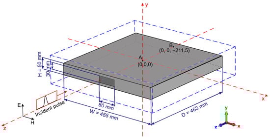
Figure 1.
Dimensions of the enclosure with aperture in the rectangular coordinate system. The electric field strength vector is directed in the +y direction. The magnetic strength vector is directed in the +x direction. Point A is the center of the enclosure. Local maxima of the electric and magnetic field strengths often occur at point B.
3. Simulation Procedure
The numerical simulation of the performance of the enclosure with an aperture as an EM shielding against a subnanosecond high-power plane-wave pulse was conducted with the Time Domain Solver of the CST Studio software equipped with the MW&RF&Optical module for modeling and comprehensive simulations of high-frequency EM fields of 3D objects [31]. More information about the simulation procedure can be found in [29,30].
4. Parameters of the Incident EM Plane Wave Pulse
The incident subnanosecond high-power EM plane-wave pulse had a Gaussian distribution of the electric and magnetic fields strengths (Figure 2). Parameters of the incident EM pulse can be found in [29,30].
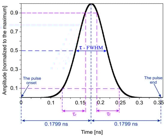
Figure 2.
The time dependence of the electric field strength (or the magnetic field strength) of the normalized incident Gaussian EM plane wave pulse.
5. Results
5.1. Development of the EM Field in the Enclosure with Aperture: 2D Vector Maps: Local Maxima of EM Field at Constant Time
The time-domain numerical simulation of the temporal and spatial development of the EM field in the shielding enclosure with aperture after interference caused by the subnanosecond high-power perpendicularly polarized EM plane wave pulse resulted in 2D and 3D, and 2D vector maps images showing the EM field development in a relatively long time of 90 ns after the pulse interference (all the images were presented in [29]). In this paper, the selected 2D images and corresponding 2D vector maps (retrieved from the 2D images) at the selected time are shown (Figure 3, Figure 4, Figure 5 and Figure 6). Figure 3, Figure 4, Figure 5 and Figure 6 were selected as representatives to analyze the distribution of the EM field in the enclosure.
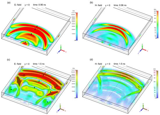
Figure 3.
2D images illustrating the development of the electric and magnetic fields in the wave phase in the enclosure at various times (at t = 0, the incident plane-wave pulse onset reaches the front plane of the enclosure). Left column—the electric field amplitude, right column—the magnetic field amplitude. Arrows show the propagation direction of the primary and secondary waves. (a,b) and (c,d) show the electric and magnetic fields at times t = 0.96 ns and t = 1.5 ns, respectively.
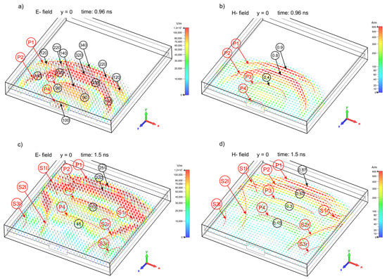
Figure 4.
2D vector maps illustrating development of the electric and magnetic fields in the wave phase in the enclosure for various times. Left column—the electric field amplitude, right column—the magnetic field amplitude. The amplitudes of the electric field at 103 V/m and magnetic field at 103 A/m are given in circles. P1, P2, P3, and P4—the primary waves, S1l, S2l, and S3l—the secondary waves formed at the left side of the enclosure; S1r, S2r and S3r—the secondary waves formed at the right side of the enclosure. (a,b) and (c,d) show the electric and magnetic fields at times t = 0.96 ns and t = 1.5 ns, respectively.
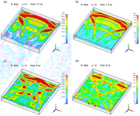
Figure 5.
2D images illustrating development of the electric and magnetic fields in the enclosure in the interference phase at various times. Left column—the electric field amplitude, right column—the magnetic field amplitude. (a,b) and (c,d) show the electric and magnetic fields at times t = 0.96 ns and t = 1.5 ns, respectively.
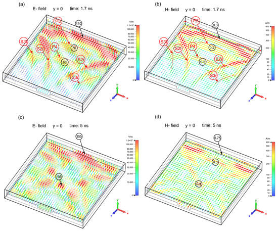
Figure 6.
2D vector maps illustrating development of the electric and magnetic fields in the enclosure in the interference phase at various times. Left column—the electric field amplitude, right column—the magnetic field amplitude. The amplitudes of the electric field in 103 V/m and magnetic field at 103 A/m are given in circles. P3 and P4—the primary waves, S2l and S3l—the secondary waves formed at the left side of the enclosure; S2r and S3r—the secondary waves formed at the right side of the enclosure. (a,b) and (c,d) show the electric and magnetic fields at times t = 0.96 ns and t = 1.5 ns, respectively.
The 2D images revealed the existence of two phases of EM field development in the shielding enclosure: a wave phase with primary and secondary waves and an interference phase in which interferences of the primary and secondary waves occur. In the wave phase, the EM field is created in the form of so-called primary (P1, P2, P3, P4) and secondary wave pulses (S1l, S1r, S2l, S2r, S3l, S3r)—Figure 3 and Figure 4. In the interference phase, the EM field has the form of temporal- and spatial-varying interference (size-limited) patterns of the associated electric and magnetic fields (Figure 5 and Figure 6). The EM field induced by the incident EM pulse in the enclosure is long-lasting compared with the incident pulse duration. The wave phase lasts approximately until the reflection of the first primary wave P1 from the rear wall (until about t = 1.54 ns). The interference phase was monitored up to t = 90 ns. After initiation, the EM field in the enclosure decreases monotonously due to the energy leakage through the aperture. At 90 ns, the amplitudes of the electric and magnetic fields decrease about 30 times compared with those of the incident EM pulse. However, they still exhibit relatively high electric (3.5 × 10⁴ V/m) and magnetic (1.5 × 10² A/m) fields.
As mentioned above, the amplitudes of the electric and magnetic fields in the enclosure are lower than that of the incident EM pulse. In the wave phase of the EM field development in the enclosure, the highest electric and magnetic fields of the primary waves occur at the centers of the waves (on the z-axis), decreasing towards the wave wings. The amplitudes of the electric and magnetic fields of the primary waves decrease when they travel from the aperture toward the rear wall (Figure 4). In the interference phase, the distributions of the electric and magnetic fields have the form of local field patterns with their own maxima. The local field pattern is formed symmetrically with respect to the z-axis (Figure 6). In addition, in the interference phase, the highest electric and magnetic fields in the enclosure occur on the z-axis, e.g., at point B (0, 0, −211.5; Figure 1). Figure 5 and Figure 6 show the local maxima of the electric and magnetic fields at point B at times t = 1.7 ns and t = 5 ns, respectively. As it was shown in [25], these local maxima at point B are the result of the constructive superpositions of the first primary wave P1 reflected from the rear wall and the second primary wave P2 traveling towards the rear wall, occurring in sequence as they travel between the front wall and rear.
5.2. Time-Dependence of the Local EM Fields: Series of the Internal EM Pulses
The time-domain simulations also provided time-dependence of the local EM amplitudes in a selected point in the enclosure. The local EM fields as a function of time are shown for two characteristic points, A (the enclosure central point) and B (the point at which the EM field often had maximum) in Figure 7 and Figure 8 (it was found in [29] that in the wave and interference phases of the EM field development, the highest electric and magnetic fields in the enclosure occurred locally on the z-axis, decreasing from the aperture towards the rear wall. This means that the most critical points in the enclosure lie along the z-axis, including points A and B. It is seen from them that in the wave phase (up to about 1.54 ns), the electric and magnetic fields at points A and B appear in the form of subnanosecond traveling pulses corresponding to passes of the primary waves through these points. In the interference phase, the nanosecond pulses that pass through points A and B are the results of the instantaneous constructive superpositions of the electric and magnetic fields, which also form subnanosecond electric and magnetic field patterns around points A and B. This means that in both phases, the electric and magnetic fields at points A and B (and presumably in other points in the enclosure) have a subnanosecond pulse character. The series of EM pulses recorded at the points in the enclosure is called internal EM pulses.
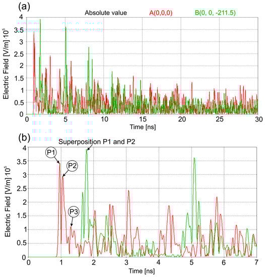
Figure 7.
Time-dependence of the electric field strength amplitude at points: A (0, 0, 0) and B (0, 0, −211.5) in the shielding enclosure with aperture after the interference of the subnanosecond high-energy EM pulse over 0–30 ns (a) and 0–7 ns (b)–the internal electric field pulses at points A and B. The internal electric field pulses labeled P1, P2, P3 (in circles) resulted from the passages of the corresponding primary waves through points A and B. Note that the electric field pulses have a duration of subnanoseconds.
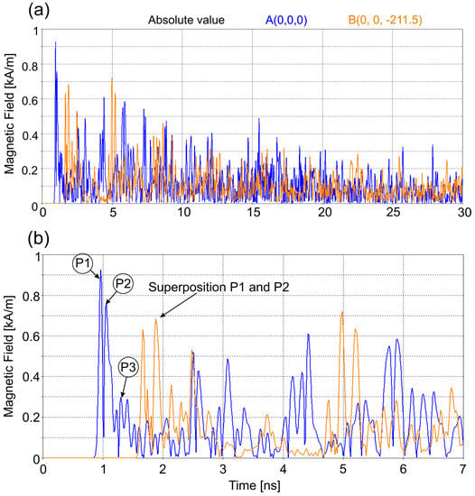
Figure 8.
Time-dependence of the magnetic field strength amplitude at points: A (0, 0, 0) and B (0, 0, −211.5) in the shielding enclosure with aperture after the interference of the subnanosecond high-energy EM pulse over 0–30 ns (a) and 0–7 ns (b) the internal magnetic field pulses at points A and B. The pulses labeled P1, P2, and P3 (in circles) resulted from the passages of the corresponding primary waves through points A and B. The pulses labeled “Superposition P1 and P2” resulted from the constructive interference of the primary waves P1 and P2 moving in opposite directions. Note that the internal magnetic field pulses have a duration of subnanoseconds.
As can be seen in Figure 7 and Figure 8, the amplitudes of the internal electric and magnetic field pulses at points A and B decrease over time. This is due to more even distributions of electric and magnetic fields over the entire area of the enclosure with increasing time and, as it is illustrated in Figure 9, due to the EM energy leakage through the aperture. The highest internal amplitudes of the electric field pulses at point A are about 3.5 × 10⁵ V/m, which is three times lower than the electric field amplitude of the EM incident pulse (106 V/m), and the highest amplitudes of the internal magnetic field pulses at the same point A are about 900 A/m, which is also three times lower than the magnetic field amplitude of the incident EM pulse (2.68 × 10³ A/m)—Figure 7 and Figure 8. Similarly, at point B the highest amplitudes of the internal electric and magnetic field pulses decrease to about 4 × 10⁵ V/m and 700 A/m, respectively. These are 2.5 and 3 times, respectively, lower than those of the electric and magnetic fields of the incident EM pulse. The internal pulse amplitudes of the electric field and the magnetic field at points A and B decrease to about 0.8 × 10⁵ V/m and 0.2 × 10³ A/m, respectively, at time t = 30 ns (and to about 0.35 × 10⁵ V/m and 0.15 × 10³ A/m, respectively, at time t = 90 ns [25]). This means that despite the shielding, the amplitudes of the internal EM pulses are high enough to cause severe malfunctions of the electronic compounds in a computer (Table 1).
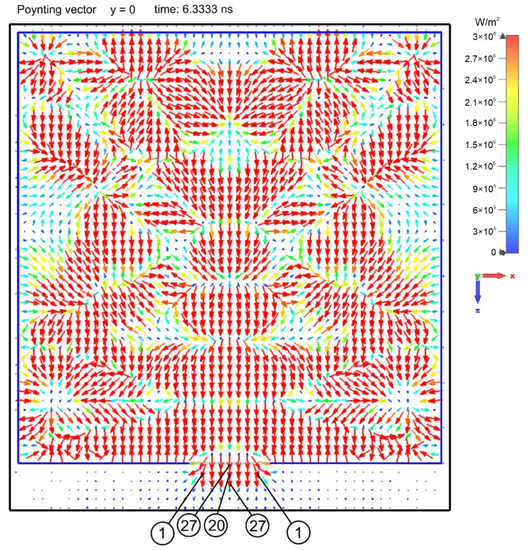
Figure 9.
Illustration of the EM energy leakage through the aperture. Vector maps showing distribution of the Poynting vectors in the enclosure in the interference phase at time t = 6.333 ns. The Poynting vectors exiting the aperture represent the EM field power density leaving the enclosure. The amplitudes of the Poynting vector in 106 W/m2 are given in circles.
The above shows that the use of the shielding enclosure with an aperture may provide substantial protection against external subnanosecond high-power EM pulse. In general, as shown above, the amplitudes of the electric and magnetic fields decrease at least three times after using the shielding enclosure with an aperture (except for the immediate area behind the aperture, as can be inferred from the detailed 2D images in [29]). However, the presence of the shielding enclosure with aperture significantly changes the nature of the influence of the EM in the space it is supposed to protect. In the case of a direct action of a subnanosecond pulse on an unsecured (i.e., in the absence of a shield) point in this space, the impact of this pulse is a one-time act. This means that the high EM field affects this point only once in a subnanosecond period. On the other hand, after applying the shielding enclosure with an aperture, the character of influence of the EM field developed in the enclosure on this point significantly increases. As shown, in the enclosure with an aperture, the series of subnanosecond internal EM pulses (with amplitudes at least 105 V/m and 2.68 × 10³ A/m) are maintained for at least 90 ns, while the one-off act of the incident EM pulse lasts only about 0.08 ns (FWHM of the incident EM pulse). This means that the point in the enclosure is influenced repeatedly over 90 ns by at least 500 subnanosecond pulses of the amplitudes lower than that of the incident EM pulse by a factor of about three to ten times. In particular, a few pulses whose amplitude is only three times lower than that of the incident EM pulse (Figure 7 and Figure 8) may pose a severe EM hazard. As shown in [32], electronic devices are more susceptible to pulses if applied with higher repetition rates. Therefore, the formation of the subnanosecond internal EM pulses in the enclosure with amplitudes differing only three times from the incident EM pulse amplitude may deteriorate the real shielding effectiveness of the enclosure with an aperture.
5.3. Performance of the Enclosure with Aperture as an EM Field Shielding
The 2D images and 2D vector maps (Figure 3, Figure 4, Figure 5 and Figure 6) showing the temporal and spatial development of the EM field inside the enclosure with aperture after irradiation with the nanosecond high-power EM plane-wave pulse make it possible to assess the effectiveness of the enclosure with an aperture as electromagnetic shielding. This can be done in two cases: locally for a selected point as a function of time and globally in the form of SE maps at various times.
5.3.1. Local SEe and SEm Versus Time
As was written above, the time-domain simulation provided time dependence of the local EM field amplitudes in a selected point in the enclosure. Using such data, it is easy to determine SEe and SEm at that point as a function of time.
Figure 10 and Figure 11 show SEe and SEm as a function of time up to t = 7 ns, respectively, at points A and B, determined using Equations (1) and (2). As can be seen in Figure 10 and Figure 11, SEe and SEm at both points pulses are at least 8 dB. They increase with time, following the decrease of the amplitudes of the electric and magnetic fields in the enclosure (Figure 7 and Figure 8). As the analysis of the numerical simulation results showed, the above tendency applies not only to points A and B but also to other points in the enclosure. However, the time-varying SEe and SEm of EM depend on the location in the enclosure.
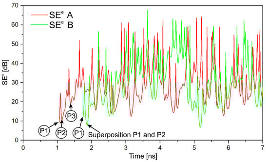
Figure 10.
Time-dependence of the shielding effectiveness SEe of the electric field at points A (0, 0, 0) and B (0, 0, −211.5) over 0–7 ns—the local SEe at points A and B. The SEe labeled P1, P2, and P3 (in circles) correspond to the passages of the primary waves P1, P2, and P3 through points A and B. The SEe labeled “Superposition P1 and P2” corresponds to the constructive interference of the primary waves P1 and P2 moving in opposite directions to each other.
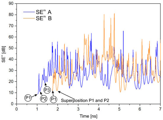
Figure 11.
Time-dependence of the shielding effectiveness SEm of the magnetic field at points A (0, 0, 0) and B (0, 0, −211.5) over 0–7 ns—the local SEe versus time. The SEm labeled P1, P2, and P3 (in circles) correspond to the passages of the primary waves P1, P2, and P3 through points A and B. The SEm labeled “Superposition P1 and P2” corresponds to the constructive interference of the primary waves P1 and P2 moving in opposite directions to each other.
5.3.2. and Maps at Constant Time
The 2D and 3D images, and, in particular, 2D vector maps obtained from our time-domain numerical calculation, enable easy calculation of and maps at constant time. Such maps give a more global view of the shielding properties of the enclosure with an aperture.
Our global approach is based on and global parameters defined (in the logarithmic scale) as follows:
and
where and are the maximum amplitudes of the electric and magnetic fields strengths of the incident EM pulse, respectively. Es (x, y, z) and Hs (x, y, z) are the amplitudes of the electric and magnetic field strengths, respectively, at time t on the same selected cross-section with shielding.
The maps of the and for the plane xz at y = 0 for several fixed times t = 0.96 ns, t = 1.5 ns, t = 1.7 ns, and t = 5 ns are plotted in Figure 12 and Figure 13. The SEg maps, presented for the first time in Figure 12 and Figure 13, enable a quick assessment of the shielding effectiveness of the tested enclosure. With SEg maps calculated for several times, it is possible to quickly identify the most critical points and determine the time trends of the shielding effectiveness in the enclosure. Such a global view is an essential advantage of using the time-domain approach in studying subnanosecond EM interferences.
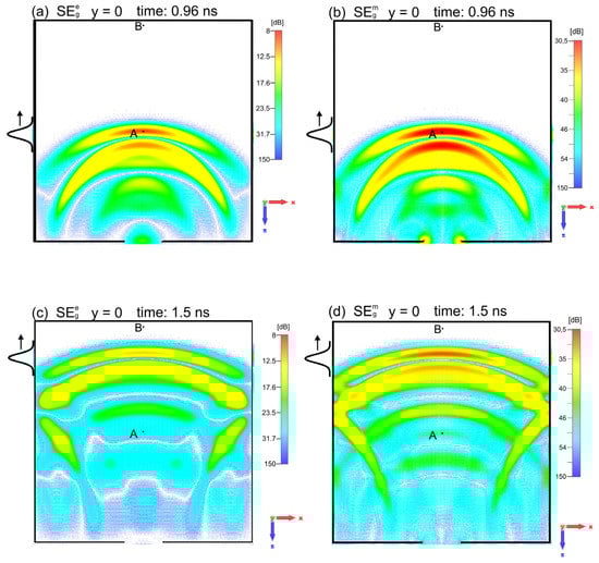
Figure 12.
Global SEg maps of the shielding effectiveness (the electric and magnetic ) at times t = 0.96 ns and t = 1.5 ns in the plane y = 0. The case of the wave phase. The position of the incident EM pulse is shown on the left side of the enclosure.
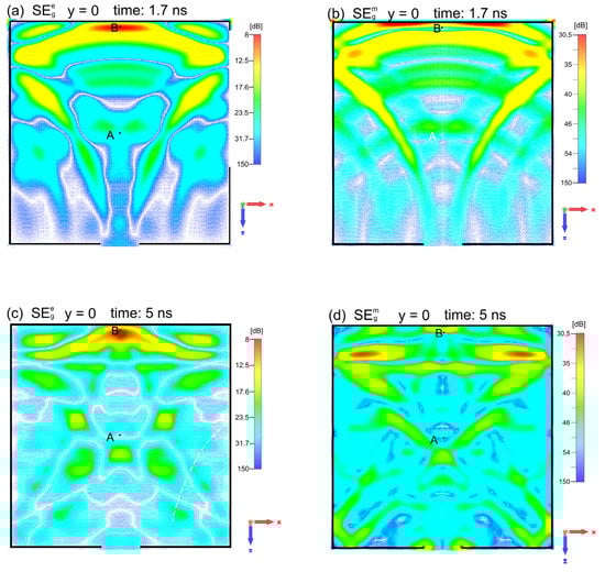
Figure 13.
Global SEg maps of the shielding effectiveness (the electric and magnetic ) at times t = 1.7 ns and t = 5 ns in the plane y = 0. The case of the interference phase.
6. Summary and Conclusions
This paper presents the results of research of the study of the performance of the enclosure with an aperture as an EM shielding against transient EM interference caused by the subnanosecond high-power perpendicularly polarized EM plane-wave pulse. The study was based on the numerical simulation in the time domain of the temporal and spatial development of the EM field in the shielding enclosure with aperture after the incident EM pulse, using the commercial code CST Microwave Studio. The time-domain simulation resulted in 2D and 3D images, and 2D vector maps of the electric and magnetic fields, which visualized the temporal and spatial development of the EM field in the enclosure over a relatively long time of 90 ns.
The results revealed the existence of two phases of the EM field development in the shielding enclosure: a wave phase and an interference phase. In the wave phase, the EM field is generated in the form of the primary and secondary wave pulses, traveling from the aperture towards the enclosure’s rear wall. In the interference phase, the EM field has the form of temporal- and spatial-varying interference patterns of the associated electric and magnetic fields, which also travel forth and back between the front and rear walls. The EM field induced by the incident EM pulse in the enclosure is long-lasting compared with the incident pulse duration. The wave phase lasts approximately until the reflection of the first primary wave from the rear wall (until about t = 1.54 ns). The next phase, the interference phase, was monitored up to t = 90 ns. Due to the EM energy leakage through the aperture and the tendency of the EM field to spread evenly throughout the enclosure, the amplitudes of the electric and magnetic fields in the enclosure decrease about 30 times within 90 ns.
The time-domain simulations also provided time-dependence of the local EM amplitudes in a selected point in the enclosure. This study of the time-varying local behavior of the EM field formed in the enclosure showed that each point in the enclosure suffers EM interference by a long series of subnanosecond internal EM pulses (of lower amplitudes than that of the incident EM pulse) passing through it over a relatively long time (at least 90 ns monitored) compared with that of the incident EM pulse duration. This means that a substantial difference in the nature of the EM interference caused by a subnanosecond high-power EM plane-wave pulse exists when a given point is not shielded and when this point is shielded by an enclosure with an aperture. The unshielded point is interfered with only once by the subnanosecond high-power EM plane-wave pulse, while the shielded point suffers EM interference by the series of subnanosecond internal EM pulses over a much longer time (at least 90 ns). The series of subnanosecond internal EM pulses may pose a severe EM hazard.
Using the time dependence of the local EM field amplitudes in a selected point in the enclosure, it was easy to determine the SEe and SEm at that point as a function of time. In other words, an evaluation of the local SEe and SEm could be performed. The results obtained show that the local SEe and SEm are at least 8 dB and increase over time.
The 2D and 3D images, and 2D vector maps calculated in the time domain for a given time enabled easy calculation of and maps for various times. Such maps, presented for the first time in this paper, are a real advancement in a more global view of the shielding properties of the enclosure with an aperture. The and maps are helpful in quickly assessing which points in the enclosure are at higher risk and how this changes with time.
The local and global approaches presented in this paper show the advantages of using the time-domain calculation for the assessment of the shielding effectiveness against ultrashort EM interference.
Author Contributions
Conceptualization, M.B. and J.M.; methodology, M.B. and J.M.; investigation, M.B. and J.M.; writing—original draft preparation, M.B. and J.M.; writing—review and editing M.B. and J.M.; visualization, M.B. and J.M.; supervision, M.B. and J.M. All authors have read and agreed to the published version of the manuscript.
Funding
The project was financed within the program of the Ministry of Science and Higher Education called “Regionalna Inicjatywa Doskonałości” in the years 2019–2022; the project number was 006/RID/2018/19, and the sum of financing was PLN 11,870,000.
Data Availability Statement
Data sharing not applicable.
Conflicts of Interest
The authors declare no conflict of interest.
References
- Sabath, F. System Oriented View on High-Power Electromagnetic (HPEM) Effects and Intentional Electromagnetic Interference (IEMI). In Proceedings of the XXIX URSI General Assembly, Chicago, IL, USA, 7–16 August 2008. [Google Scholar]
- Giri, D.V.; Tesche, F.M. Classification of Intentional Electromagnetic Environments (IEME). IEEE Trans. Electromagn. Compat. 2004, 46, 322–328. [Google Scholar] [CrossRef]
- IEC 61000-2-13; Electromagnetic Compatibility (EMC)—Part 2-13: Environment—High-Power Electromagnetic (HPEM) Environments—Radiated and Conducted, First Edition 2005-03. International Standard IEC: Geneva, Switzerland, 2005.
- Giri, D.V.; Tesche, F.M. An Overview of High-Power Electromagnetic (HPEM) Radiating and Conducting Systems. URSI Radio Sci. Bull. 2006, 318, 6–12. [Google Scholar]
- Kopp, C.; Pose, R. The Impact of Electromagnetic Radiation Considerations on Computer System Architecture; Dept of Computer Science, Monash University: Clayton, VIC, Australia, 2016. [Google Scholar]
- Sabath, F. Threads of Electromagnetic Terrorism. In Proceedings of the EUROEM 2012—ONERA, Toulouse, France, 2–6 July 2012. [Google Scholar]
- High Power Microwave Technology and Effects; A University of Maryland Short Course Presented to MSIC Redstone Arsenal, Alabama August 8–12, 2005; University of Maryland: College Park, MD, USA, 2005.
- Hwang, S.M.; Hong, J.I.; Huh, C.S. Characterization of the susceptibility of integrated circuits with induction caused by high power microwaves. Prog. Electromagn. Res. 2008, 81, 61–72. [Google Scholar] [CrossRef]
- Xie, F.; Cao, B.; Liu, C.L. Damage efficiency research of PCB components under strong electromagnetic pulse. Appl. Mech. Mater. 2012, 130–134, 1383–1386. [Google Scholar] [CrossRef]
- Nitsch, D.; Sabath, F.; Schmidt, H.-U.; Braun, C. Comparison of the HPM and UWB Susceptibility of Modern Microprocessor Boards. In Proceedings of the 15th International Zurich Symposium on EMC 2003, Zurich, Switzerland, 18–20 February 2003. [Google Scholar]
- Baum, C.E.; Nitsch, D.H. Band Ratio and Frequency Domain Norms; Interaction Notes 584; Air Force Office of Scientific Research, Wright-Patterson Air Force Base: Montgomery, OH, USA, 2003. [Google Scholar]
- IEEE Standard 299.1-2013; IEEE Standard Method for Measuring the Shielding Effectiveness of Enclosures and Boxes Having all Dimensions Between 0.1 m and 2 m. IEEE: New York, NY, USA, 2014.
- Diendorfer, G. Induced voltage on an overhead line due to nearly lightning. IEEE Trans. Electromagn. Compat. 1979, EMC-32, 292–299. [Google Scholar]
- Chen, J.Y.; Gandhi, O.P. Currents induced in an anatomically based model of a human for exposure to vertically polarized electromagnetic pulses. IEEE Trans. Microw. Theory Tech. 1991, 39, 31–39. [Google Scholar] [CrossRef]
- IEEE Standard 299; Standard Method for Measuring the Effectiveness of Electromagnetic Shielding Enclosures. IEEE: New York, NY, USA, 2007.
- Dawson, J.F.; Marvin, A.C.; Robinson, M.P.; Flintoft, I.D. On the meaning of enclosure shielding effectiveness. In Proceedings of the 2018 International Symposium on Electromagnetic Compatibility (EMC EUROPE), Amsterdam, Netherlands, 27–30 August 2018; pp. 746–751. [Google Scholar]
- Kubik, Z.; Skála, J. Shielding effectiveness simulation of small perforated shielding enclosures using FEM. Energies 2016, 9, 129. [Google Scholar] [CrossRef]
- Shourvarzi, A.; Joodaki, M. Shielding Effectiveness Estimation of a Metallic Enclosure With an Aperture Using S-Parameter Analysis: Analytic Validation and Experiment. IEEE Trans. Electromagn. Compat. 2016, 59, 537–540. [Google Scholar] [CrossRef]
- Ren, D.; Du, P.A.; He, Y.; Chen, K.; Luo, J.W.; Michelson, D.G. A fast calculation approach for the shielding effectiveness of an enclosure with numerous small apertures. IEEE Trans. Electromagn. Compat. 2016, 58, 1033–1041. [Google Scholar] [CrossRef]
- Celozzi, S.; Araneo, R. TD-Shielding effectiveness of enclosures in presence of ESD. In Proceedings of the 2013 International Symposium on Electromagnetic Compatibility, Brugge, Belgium, 2–6 September 2013; pp. 541–544. [Google Scholar]
- Celozzi, S. New figures of merit for the characterization of the performance of shielding enclosures. IEEE Trans. Electromagn. Compat. 2004, 46, 142. [Google Scholar] [CrossRef]
- Klinkenbusch, L. On the shielding effectiveness of enclosures. IEEE Trans. Electromagn. Compat. 2005, 47, 589–601. [Google Scholar] [CrossRef]
- Araneo, R.; Celozzi, S. Toward a definition of the shielding effectiveness in the time-domain. In Proceedings of the 2013 IEEE International Symposium on Electromagnetic Compatibility, Denver, CO, USA, 5–9 August 2013; pp. 113–117. [Google Scholar]
- Celozzi, S.; Araneo, R. Alternative definitions for the time-domain shielding effectiveness of enclosures. IEEE Trans. Electromagn. Compat. 2014, 56, 482–485. [Google Scholar] [CrossRef]
- Araneo, R.; Attolini, G.; Celozzi, S.; Lovat, G. A global approach to time-domain shielding problems. In Proceedings of the 2014 IEEE International Symposium on Electromagnetic Compatibility (EMC), Raleigh, NC, USA, 4–8 August 2014; pp. 86–90. [Google Scholar]
- Cai, X.; Sun, X.; Zhao, X. A total energy reduction shielding effectiveness description for enclosures. Int. J. Appl. Electromagn. Mech. 2016, 50, 283–295. [Google Scholar] [CrossRef]
- Araneo, R.; Attolini, G.; Celozzi, S.; Lovatt, G. Time–domain Shielding Performance of Enclosures: A Comparison of Different Global Approaches. IEEE Trans. Electromagn. Compat. 2016, 58, 434–441. [Google Scholar] [CrossRef]
- Araneo, R.; Celozzi, S. Actual Performance of Shielding Enclosures. In Proceedings of the 2004 International Symposium on Electromagnetic Compatibility (IEEE Cat. No.04CH37559), Silicon Valley, CA, USA, 9–13 August 2004; Volume 2, pp. 539–544. [Google Scholar]
- Budnarowska, M.; Mizeraczyk, J. Temporal and Spatial Development of the EM Field in a Shielding Enclosure with Aperture after Transient Interference Caused by a Subnanosecond High-Energy EM Plane Wave Pulse. Energies 2021, 14, 3884. [Google Scholar] [CrossRef]
- Budnarowska, M.; Mizeraczyk, J.; Bargieł, K. Development of the EM Field in a Shielding Enclosure with Aperture after Interference Caused by a Subnanosecond High-Power Parallelly Polarized EM Plane Wave Pulse. Energies 2022, 16, 585. [Google Scholar] [CrossRef]
- CST Studio Suite. Available online: www.cst.com (accessed on 1 November 2022).
- Korte, S.; Garbe, H. Breakdown Behaviour of electronics at variable pulse repetition rates. Adv. Radio Sci. 2006, 4, 7–10. [Google Scholar] [CrossRef]
Disclaimer/Publisher’s Note: The statements, opinions and data contained in all publications are solely those of the individual author(s) and contributor(s) and not of MDPI and/or the editor(s). MDPI and/or the editor(s) disclaim responsibility for any injury to people or property resulting from any ideas, methods, instructions or products referred to in the content. |
© 2023 by the authors. Licensee MDPI, Basel, Switzerland. This article is an open access article distributed under the terms and conditions of the Creative Commons Attribution (CC BY) license (https://creativecommons.org/licenses/by/4.0/).