Article

Digital System Performance Enhancement of a Tent Map-Based ADC for Monitoring Photovoltaic Systems

Department of Engineering & Technology, University of Huddersfield, Huddersfield HD1 3DH, UK
*
Author to whom correspondence should be addressed.
Electronics 2020, 9(9), 1554; https://doi.org/10.3390/electronics9091554
Submission received: 31 August 2020 / Revised: 15 September 2020 / Accepted: 18 September 2020 / Published: 22 September 2020
(This article belongs to the Special Issue Reliability Analysis for Photovoltaic Systems)

Abstract

:
Efficient photovoltaic installations require control systems that detect small signal variations over large measurement ranges. High measurement accuracy requires data acquisition systems with high-resolution analogue-to-digital converters; however, high resolutions and operational speeds generally increase costs. Research has proven low-cost prototyping of non-linear chaotic Tent Map-based analogue-to-digital converters (which fold and amplify the input signal, emphasizing small signal variations) is feasible, but inherent non-ideal Tent Map gains reduce the output accuracy and restrict adoption within data acquisition systems. This paper demonstrates a novel compensation algorithm, developed as a digital electronic system, for non-ideal Tent Map gain, enabling high accuracy estimation of the analogue-to-digital converter analogue input signal. Approximation of the gain difference compensation values (reducing digital hardware requirements, enabling efficient real-time compensation), were also investigated via simulation. The algorithm improved the effective resolution of a 16, 20 and 24 Tent Map-stage analogue-to-digital converter model from an average of 5 to 15.5, 19.2, and 23 bits, respectively, over the Tent Map gain range of 1.9 to 1.99. The simulated digital compensation system for a seven Tent Map-stage analogue-to-digital converter enhanced the accuracy from 4 to 7 bits, confirming real-time compensation for non-ideal gain in Tent Map-based analogue-to-digital converters was achievable.

1. Introduction

The ability to detect small variations at high speeds in analogue signals is a key requirement for data acquisition (DAQ) systems when highly frequent, precise, and accurate measurements (with lower uncertainty) need to be made. DAQ systems typically require high resolution analogue-to-digital converters (ADCs) to detect small signal variations, however, higher resolutions and operational speeds generally increase the cost of the DAQ system [1,2].
Many photovoltaic (PV) systems necessitate analogue signals from sensors to be sampled and converted to the digital domain to enhance the reliability of energy delivery. One such example is their employment in battery energy storage systems (BESSs) [3]. BESSs require careful monitoring of bus and cell voltage, current, and temperature, to determine the state of charge (SoC) and prevent over-charging and deep discharging of the batteries, which impacts their lifespan [3]. One popular battery technology is lithium iron phosphate, which has very linear voltage to capacity per ampere-hour curves (there is a change of less than 100 mV over a 10 to 90% capacity), making determining the SoC of the battery from this measurement alone challenging [4]. Being capable of detecting smaller variations in the cell voltage could aid more precise battery management, improve SoC predictions, and increase battery lifespan.
The ability to detect small signal variations, especially over a relatively large signal range, would also be beneficial for non-intrusive load monitoring for a residential PV system. DAQ systems capable of detecting small signal variations over a large measurement range would enable more accurate and precise analysis of the acquired energy signatures. This would allow the consumer to determine where the energy being generated by the PV module (and imported from the grid) is being used down to specific appliances including some very low power devices. This facility would be beneficial to the consumer enabling unnecessary energy usage to be identified and reduced, thus aiding the reduction of peak load demand [5].
Recent research has proven the possibility of prototyping non-linear chaotic Tent Map (TM)-based ADCs using low-cost discrete components rather than fabricating on silicon (an expensive process [6]) to achieve acceptable performance [7,8]. ADCs employing TMs within the conversion process continuously fold and amplify the input signal making them well-suited for the detection of small signal variations over a large signal range [7]. Most other ADC architectures do not amplify the input signal during the conversion process which restricts the size of signal variation capable of being detected. However, a significant limitation of the TM-based ADC is the non-ideal TM stage gain, which has previously restricted adoption within DAQ systems due to the effect on the ADC output accuracy.
TM-based ADCs are based on conversion circuitry which symmetrically folds and amplifies an input signal by a factor between 1 and 2 inclusive [9] (as demonstrated in Figure 1). Two TM-based ADCs capable of detecting 20 µV changes over a relatively large voltage range of 0–10 V were developed by Berberkic [7]. One of the ADC architectures had the TMs arranged in a series configuration, while the other had a single TM in a feedback configuration. In both implementations, inexpensive commercial 10–12-bit ADCs were employed to acquire the TM output signals and thus determine the digital output. The integral TMs blocks, in the structures, were constructed from discreet, off-the-shelf components, making these ADCs inexpensive to prototype (compared to if they were fabricated in silicon) [7]. Series and feedback configurations of TM ADCs were also constructed by Upton et al. and Liu et al., respectively [8,10]. These ADCs employed comparators in place of ADCs to determine the digital output from the TM output signals, restricting the potential resolution that could be achieved. The ADC devised by Upton et al. was also inexpensive to prototype, being constructed out of discreet components [8]. Meanwhile, the ADC developed by Liu et al. was developed to be fabricated onto silicon to enable a more precise TM gain to be produced [10].
The absolute accuracy of all TM-based ADCs is affected by two main factors: non-ideal TM gain and noise [11,12] (this paper focuses on addressing the former). The discussed TM-based ADCs rely on the folded signals being amplified back to full scale, thus the TM gains must be exactly 2. When the TM gain is less than 2, the accuracy of the TM-ADCs is significantly affected [11], as illustrated in Figure 2 and Table 1, which demonstrates how a 0.5 and 5% reduction in the TM gain of such an ADC affects the accuracy. The loss in accuracy is due to a reduction in the TM gain resulting in missing or incorrect digital output codes being produced, as demonstrated in Figure 1 and Table 2.
Achieving an exact, ideal TM gain of 2, in a practical hardware implementation, is impossible due to component tolerances. Although components with low tolerances can be employed to improve the gain precision, this generally leads to an increase in cost. In addition, the gain values of the TM-based ADC will continue to vary over time with temperature fluctuations [14]. An alternative solution, therefore, is to evaluate the effects non-ideal TM gain has on the performance of a TM-based ADC output and compensate for it through post-processing of the data, thus enabling the enhanced estimation of the initial conditions (the analogue input signal) from the digital ADC output. The eventual aim for this research is to employ an algorithm to estimate changes in TM gains from the ADC output (similar to that proposed by Dutta et al. [15]) and then estimate the initial conditions, thus producing a self-calibrating ADC.
TMs structures are constructed through the implementation of two difference equations, as shown in Equation (1), where µ is the TM gain, xn the input, and xn+1 the output [9]. By estimating the initial conditions (i.e., the amplitude of the original input signal) the loss in the output accuracy of a TM-based ADC, due to non-ideal µ, can be recovered. However, TMs are non-invertible and non-linear [9], which complicates the process of estimating initial conditions. There is a considerable body of literature on estimating the initial conditions of TMs; however, little is recent and a significant amount explores estimating the initial conditions of chaotic signals superimposed with noise (a constant issue with chaotic communication systems) [16,17,18]. Although noise is an issue for TM-based ADC implementations [12], these techniques are for a different variation of the TM function known as a skew-TM [16,17,18]. This variation of the chaotic map (and thus the referenced techniques) is unsuitable for electronic circuit implementation and for use within an ADC.
x n   +   1   =   { μ x n μ ( 1     x n )   when   x n   <   0.5 x n     0.5
Research undertaken to estimate the initial conditions of the TM function given in Equation (1) is limited and intermittent, especially methods which consider non-ideal µ. One method, proposed by Xi et al. [19], estimated the initial conditions using the sawtooth and Bernoulli map functions. Although this approach would be simple to implement as a digital system, it was deemed unsuitable for compensating for the non-ideal µ as it assumes the µ was exactly 2 [19].
Another method that would be implementable as a digital system was proposed by Litovski et al. [20]. This method attempted to compensate for non-ideal µ by multiplying the TM-ADC output (after being converted to binary and then the equivalent voltage levels) with a scalar value. The scalar value was the ratio between the partition point voltage and the equivalent voltage of the ADC output; the partition point voltage determines when the next difference equation, in a chaotic map function, must be employed. The main disadvantage with this approach is that TMs are non-linear, thus multiplying the ADC output by a fixed scalar value would cause the compensated results to have inconsistent improvements in accuracy when supplied with different input voltages [20].
A more accurate initial condition estimation method was proposed by Basu et al. [21] who calculated the effective difference between the voltage levels for ideal and non-ideal µ that each bit of the ADC output represented. However, this approach was more complex and challenging to implement as a digital system, as the algorithm involved calculating floating point numbers, using multiplication and division, for n iterations (n is the ADC resolution) and requires more computational overhead than the previous two examples [21].
The aim of this paper is to evaluate a novel algorithm of estimating the initial conditions of a TM-based ADC when the mean µ is known. Similar to the algorithm proposed by Basu et al. [21], this algorithm determines the difference between the voltage levels that each bit represents for the actual and ideal µ. However, the proposed algorithm requires less computational overhead enabling a simpler digital system implementation. The paper assesses the effectiveness of the algorithm through simulation and whether it would be implementable onto a field programmable gate array (FPGA) so that a practical, real-time, digital compensation system can be developed resulting in a high-precision ADC. Methods of approximating values for the algorithm (to reduce resource consumption when implemented onto an FPGA) are also assessed, in addition to a sensitivity analysis investigating the effectiveness of the algorithm when the estimated µ is not equal to that of the TM-based ADC. By achieving this, further signal processing could be performed on the FPGA, producing a low-cost DAQ system (the set-up is presented in Figure 3).
Principal conclusions drawn from this research were: the algorithm was able to improve the effective resolution of the TM-based ADC; implementing the algorithm as a real-time, digital, compensation system was possible; the algorithm was as effective as the algorithm proposed by Basu et al. [21]; the difference values that require calculating can be estimated using fewer hardware resources; and the sensitivity analysis highlighted the need for an investigation into high accuracy µ estimation, when employing the compensation algorithm for higher staged TM-based ADCs.
The paper is structured as follows. Section 1 provides an overview of the work already undertaken to determine the initial conditions from chaotic systems employing TMs. The algorithm being assessed and its testing is described in Section 2, and Section 3 presents the results. A discussion of the results is given in Section 4 and conclusions are drawn. Finally, Appendix A provides lists and descriptions of all the acronyms, symbols and key terminologies employed in this paper.

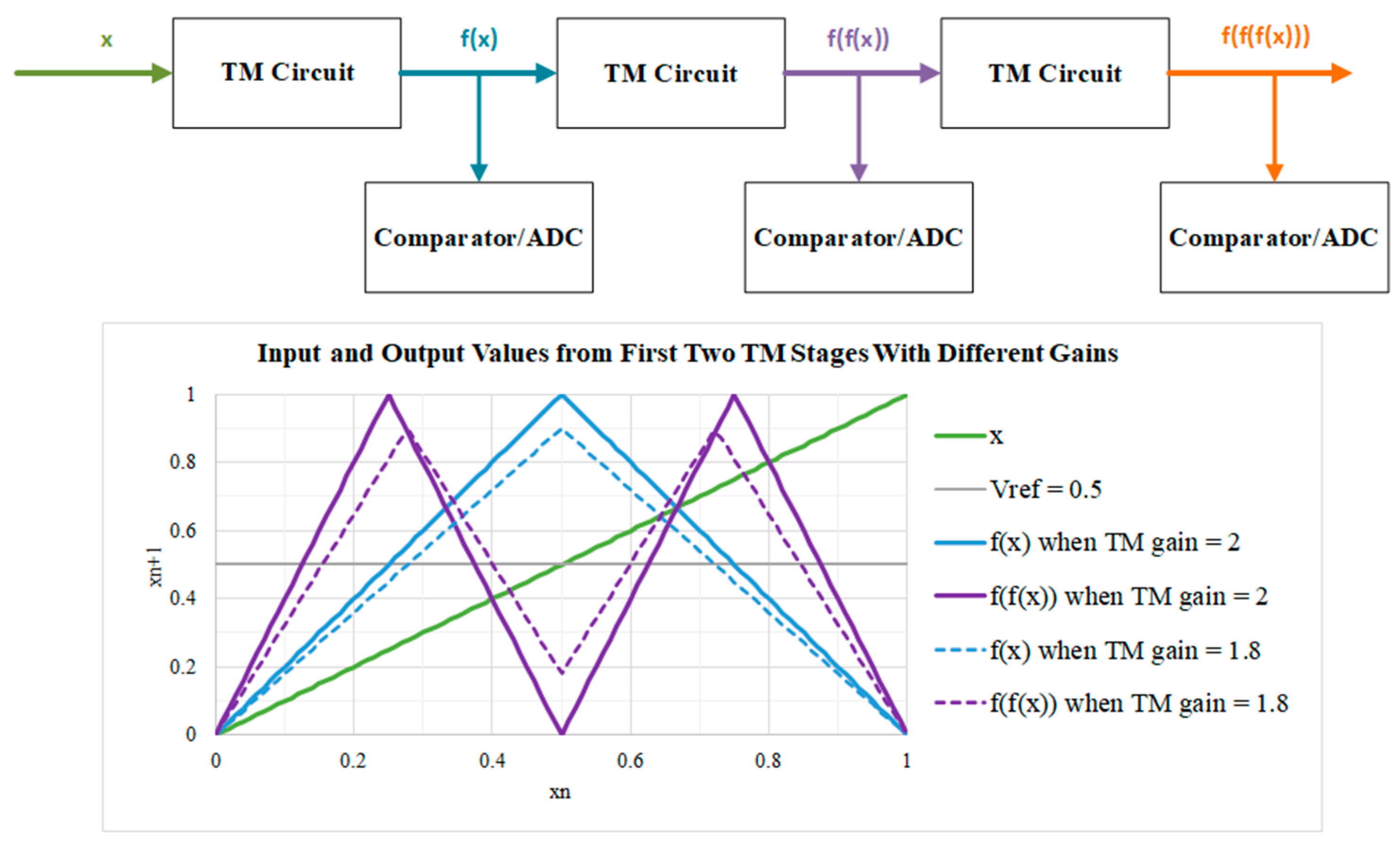
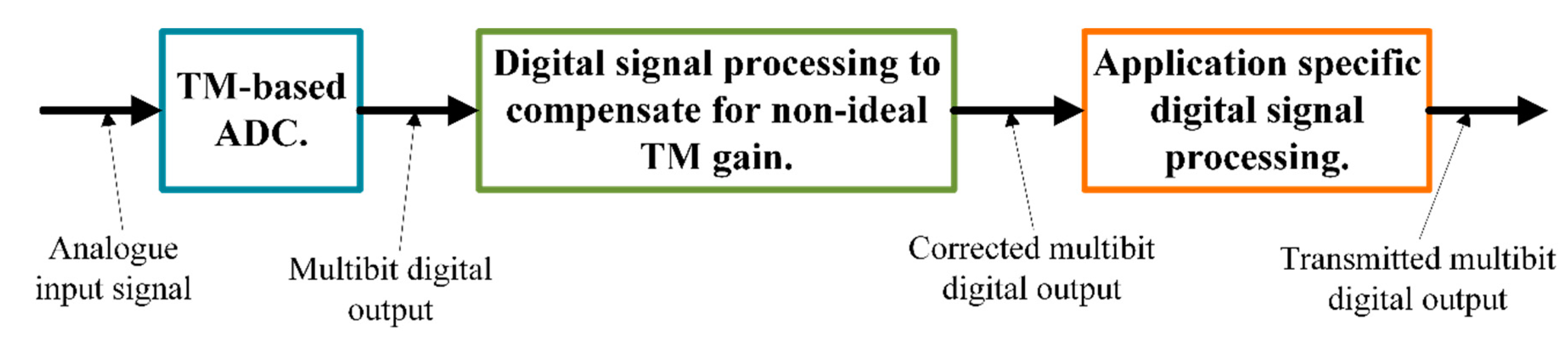
2. Materials and Methods

Figure 4 presents the proposed design for the TM-based ADC and compensation system. The TM-based ADC is based on the design developed by Upton et al. [8] which is inexpensive to implement in hardware. The ADC samples the analogue signal, which then propagates through a series of comparators and TM circuits to determine the equivalent digital output (which is in Gray-code representation). After the sampled signal passes through the first comparator and TM circuit, the ADC acquires a further sample. An FPGA samples and aligns the comparator outputs, before converting the Gray-code words into binary. Finally, the FPGA compensates for non-ideal µ in the ADC by performing the compensation algorithm on the aligned, ADC output. This final part will be executed before the subsequent sample has been converted to binary, thus achieving real-time compensation for non-ideal TM gain.
This paper presents the results from the tests undertaken to assess the effectiveness of this compensation algorithm. Section 2.1 describes the operation of the algorithm, while Section 2.2 details the tests undertaken.

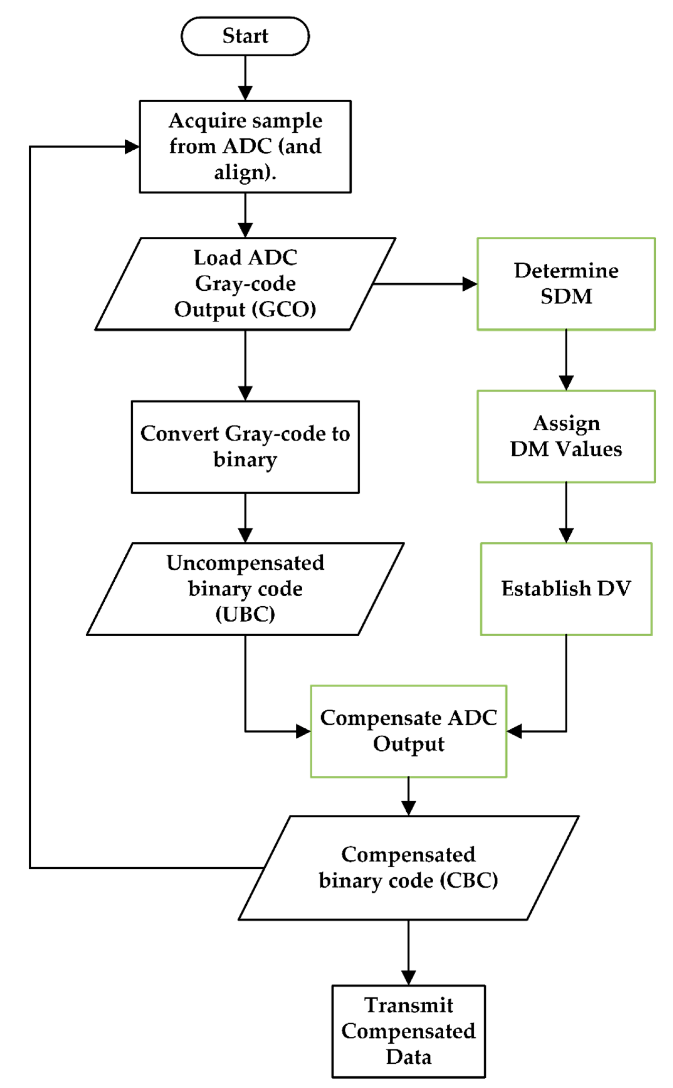
2.1. The Compensation Algorithm

The compensation algorithm for non-ideal µ within the TM-based ADC has 4 key stages:
  • Determine the sign for difference measure (SDM) to establish the direction of difference between the ideal output and that due to the non-ideal gain for each TM stage.
  • Calculate the difference measure (DM) to determine the magnitude of difference between the ideal output and that due to the non-ideal gain for each TM stage.
  • Compute the difference value (DV), which provides the overall magnitude and direction of the cumulative difference between the non-ideal gain of the TM based ADC output and the ideal.
  • Compensate the ADC output.
This algorithm (summarized and highlighted green in Figure 5 and Figure 6) requires the partition point voltage to be halfway between the valid ADC input range, and for the mean µ to be known and less than 2. The ADC output, similar to that proposed by Upton et al. [8], is also in Gray-code format.
The first stage of the algorithm determines if a DM needs to be added to, or subtracted from, the equivalent weighting for each bit, using the Gray-code ADC output. The most significant bit (MSB) requires no compensation as it is established before the input signal goes through the first TM stage, while the SDM representing the second MSB will always be positive (logic high) as µ will be less than 2 (i.e., the ideal gain).
The magnitude of each DM value is calculated in the second stage, where Equation (2) is used to calculate the DMs, providing the corresponding bits in the ADC output are logic high, otherwise the DM is set to 0. The two extremes of the valid input voltage range are denoted by Vcc and Vee, the mean TM gain by µ, and the individual bit being considered by i (where 1 is the MSB).
DM   =   ( V cc     V ee ) ( 1 μ i     1     1 2 i     1   )
The third stage of the compensation algorithm sums the DM values (taking into consideration the individual polarity determined in the first stage) to calculate the DV. Stage four takes the ADC output (converted to binary code) and adds/subtracts the DV to compensate for the non-ideal µ during the analogue-to-digital conversion process.

2.2. Methodology

2.2.1. Analysis of the Algorithm

A model of the TM-ADC was developed in MATLAB R2019b to emulate the practical performance of the TM-based ADC in [8], and initially configured to have 16 TM circuits (stages), a valid input signal range of 0–3 V, and a sampling rate of 25 MHz. The ADC was then supplied with a 0–3 V ramp input signal at 380 Hz (generated using the sawtooth function from the Signal Processing Toolbox). The sampling frequency value and valid input voltage range were chosen to match those of [8], whilst the input signal frequency was set, as a representative value, low enough that an ideal, 16-stage TM-based ADC could sample every step change within the signal. A reasonably high number of TM stages were modelled to demonstrate the effectiveness of the algorithm.
The lower the µ, the further the TM output from the ideal, resulting in the algorithm being less effective at compensating for the non-ideal gain due to the increase in the number of missing codes (i.e., lost data) which cannot be compensated for as accurately. Therefore, the lowest gain that this algorithm was tested with was set to 1.9, because this was also deemed achievable in a practical implementation. The output of the ADC was then compensated for using the algorithm and the improvement in effective resolution noted. The µ was incremented by 0.01 and the test repeated until the µ equaled two.
The above test was repeated two more times with the TM-based ADC model configured to have 20 and 24 TM stages, to analyze the effectiveness of the algorithm when the number of TM stages was increased. Figure 7 presents a flow diagram detailing how the MATLAB script developed for the test was structured.

2.2.2. FPGA Implementation

The algorithm was then implemented into the Very high speed integrated circuits Hardware Description Language (VHDL) code originally developed for the fundamental ADC employed in [8] which aligns and converts the sampled ADC output data to binary code. The VHDL implementation of the algorithm was developed for an ADC with 7 TM stages (with a mean µ of 1.9), as the focus of this research is to eventually compensate for non-ideal gain within a prototype, 7-stage electronic implementation of the TM-based ADC and confirm real-time compensation is possible.
The algorithm was implemented so it would be applied to the converted ADC sample (see Figure 8) before the next input sample is converted to binary, thus achieving real-time compensation for non-ideal µ. The DM values used by the algorithm for each bit were also calculated using Equation (2), converted to binary, and placed into an array within the VHDL code.
A model of the TM-based ADC that mimicked how the ADC samples and outputs the acquired data, was also developed in VHDL to test the algorithm. A test bench VHDL program was then developed to write and save the uncompensated and compensated values from the implemented algorithm into two separate texts files when it was being tested via simulation using the ModelSim FPGA software. Figure 8 and Figure 9 display how the VHDL components were connected for simulation.

2.2.3. Comparison with Basu et al.’s Method

The effectiveness of the compensation algorithm discussed in Section 2.2.1 was compared with that developed by Basu et al. [21] using the MATLAB code provided in [22] to analyze their algorithm [22]. Figure 10 presents how the MATLAB script was modified to repeat the tests described in Section 2.2.1 using Basu et al.’s algorithm.

2.2.4. Approximation of Difference Values

The focus of this research was to compensate for non-ideal µ within the TM-based ADC; however, when TM functions are implemented as electronic circuits, the gain values vary over time with temperature fluctuations [14]. There is a desire to estimate the µ from the ADC output and then apply the compensation algorithm, thus producing a self-calibrating ADC. This would require implementing Equation (2) onto an FPGA to calculate the DM values for the algorithm, but this would be resource intensive, especially when employed with higher resolution ADCs. For this reason, two more resource efficient methods of approximating the DM values were compared.
The first method (the straight-line and error approximation) involved taking a straight-line approximation of the ideal DM values versus µ curves (over a 1.95 ≤ µ ≤ 2.0 range) for each bit. The gradients of the straight-line approximations were calculated using the end points of the DM versus µ plots (as shown in Figure 11 for the least significant bit (LSB)) because this approach was found to achieve closer approximations of the DM values rather than estimating the gradient using a line of best fit. The constant for the main straight-line approximation was determined using the DM values when µ = 2.
The difference between the approximated and ideal DM values were then determined to calculate the errors. Two straight-line approximations of the error versus µ curves (one for 1.9 ≤ µ ≤ 1.95 and the other for 1.95 ≤ µ ≤ 2.0) were also taken (see Figure 12) and added to the initial straight-line approximation to improve accuracy. For both error approximations the constant value was calculated when µ = 1.95.
The second method (the scalar approximation method) involved taking the ideal DM values for a chosen µ and multiplying by a scalar value determined using Equation (3) (where µc is the actual gain of the TM circuit and µo is the gain employed in the ideal DM, Equation (2)).
Scalar   =   1     μ c     μ o 2     μ o
Both methods were tested over a 1.9 ≤ µ ≤ 2.0 (in 0.01 increments) range because ideally the average TM-ADC gain range should be within this region to achieve the highest effective resolution after compensation. The scalar approximation method was tested using the µo values of 1.9 and 1.95. The test outlined in Section 2.2.1 was repeated using these two methods to approximate the DM values for a 16 stage TM-based ADC only.

2.2.5. Sensitivity Analysis of Algorithm

There will always be a set amount of uncertainty when establishing the mean µ of a TM-based ADC. To investigate the effects this uncertainty might have on the ability of the algorithm to compensate for non-ideal µ within the ADC, a sensitivity analysis was performed.
The sensitivity analysis involved adapting the MATLAB code employed in the test detailed in Section 2.2.1, to investigate how well the algorithm improved the effective resolution of the TM-based ADC with different inherent µ, whilst the µ the algorithm employed was fixed. The test initially involved compensating for an 8-stage TM-based ADC with a range of µ (µADC) from 1.9 to 2.0. The compensation algorithm was then applied to the ADC output, employing a µ of 1.96 to determine the DM values. The µADC was then incremented by 0.001 and the process repeated. This test was then replicated with a 16-stage TM based ADC. Figure 13 presents a flow diagram detailing how the MATLAB script was adapted to perform the sensitivity analysis.

3. Results

3.1. Analysis of the Algorithm

Figure 14 presents the effective resolution of the 16-, 20-, and 24-stage TM-based ADCs output (before and after compensation) over a 1.9 ≤ µ ≤ 2 range when using Equation (2) to determine the DM values. The results highlight that when 1.9 ≤ µ ≤ 1.99, the effective resolution of the uncompensated ADC was identical for all three models. In addition, when µ = 2 (i.e., ideal) the effective resolution equaled the number of TM stages within the ADC model. When the compensation algorithm was applied to the output of the 16-, 20-, and 24-stage ADC models there was a minimum increase in the effective resolution of 9, 13, and 17 bits, respectively.
The difference (in step size) between the input and equivalent output signals of the simulated 16 TM-stage ADC, when µ was 1.9, is also presented in Figure 15. The plot highlights the non-linear nature of TMs and both Figure 14 and Figure 15 demonstrate how small decreases in the gain of a TM-based ADC significantly affect the ADC output accuracy.

3.2. FPGA Implementation

Figure 16 presents a graph of the difference between the input and equivalent output voltage signals from the simulated VHDL module before and after the algorithm was applied. The VHDL module consisted of: a model, seven-stage TM-based ADC (supplied with a ramp input signal); the original VHDL code developed for [8] to align and convert the ADC Gray-code output to binary; and the VHDL code implementation of the algorithm described in Section 2.1. Figure 16 highlights a maximum improvement of 3 bits in the effective resolution of the ADC. In addition, the compensation algorithm was performed on each newly acquired sample of the input signal while the next sample was obtained, confirming that real-time compensation of non-ideal µ is possible.

3.3. Comparison with Basu et al.’s Method

Figure 17 shows a graph comparing the effective resolution of the 16-, 20-, and 24-stage TM-based ADC MATLAB models over a 1.9 ≤ µ ≤ 2 range. The graph compares the ADC effective resolution without compensation, with compensation using the algorithm discussed in Section 2.1, and with compensation using the algorithm developed by Basu et al. [21], and shows both compensation algorithms are identical in performance with regards to improving the effective resolution of the ADC.

3.4. Approximation of Difference Values.

Figure 18 presents the effective resolution of the 16-stage ADC output (before and after compensation) over a 1.9 ≤ µ ≤ 2 range, when using Equation (2) and both approximation methods to determine the DM values. Overall, the straight-line approximation method attained more accurate results, although the scalar approximation method achieved identical performance when µo = 1.95 and µ ≥ 1.94.

3.5. Sensitivity Analysis of Algorithm

Figure 19 and Figure 20 present the results from the sensitivity analysis, which explores how uncertainty in determining the µADC for an 8- and 16-TM-stage TM-based ADC affects the ability of the compensation algorithm to improve the effective resolution. The µ of the 8-stage TM-based ADC models ranged from 1.9 to 2 (in increments of 0.001), while the µ employed by the algorithm was 1.96.
The results demonstrate a sharper roll-off in the effective resolution of the 16-stage ADC compared to the 8-stage ADC. In addition, both plots showed the compensation algorithm still improved the overall effective resolution of the ADC when µADC was less than 1.972 and 1.976 for the 8-stage and 16-stage TM-based ADC, respectively.

4. Discussion and Conclusions

The novel TM-based ADC algorithm, for the compensation of non-ideal TM-stage gain, is detailed in this paper. When using the ideal DM parameter values calculated using Equation (2), the compensation algorithm improved the effective resolution of a 16-, 20-, and 24-stage ADC by an average of 10.5, 14.2, and 18 bits, respectively, over a 1.9 ≤ µ ≤ 1.99 range, giving an average effective resolution of 15.5, 19.2, and 23 bits, respectively. It is noted that the further µ is from the ideal value of 2, the less effective the compensation algorithm, hence once µ falls below a certain value (1.95, 1.96, and 1.97 for 16-, 20-, and 24-stage ADC, respectively) it is impossible for the algorithm to increase the effective resolution to the same level as the ideal gain due to the number of missing codes. Achieving a µ > 1.9 will be possible in a circuit implementation, thus the algorithm will not be attempting to compensate for further losses in the ADC output accuracy.
The results from the FPGA implementation of the compensation algorithm demonstrates a 3-bit improvement in the ADC effective resolution from 4 to 7 bits. In addition, this was possible even though the calculated DM values were converted to binary code and rounded, thus losing some potential accuracy in the compensation values. Finally, each ADC input sample is compensated for non-ideal µ before the next sample has finished being processed, confirming that a practical, real-time compensation system for improving the accuracy of a TM-based ADC could be implemented.
Figure 17 shows that the compensation algorithm analyzed in this paper was as effective as the algorithm developed by Basu et al. [21] with no difference in the effective resolution of the compensated ADC output. The proposed algorithm also has the benefit of not requiring the constant recalculation of floating-point variables for each bit of the digital outputs, meaning fewer computational resources and enabling real-time compensation (as confirmed by the simulation results in Section 3.2).
The method of approximation of the DM values which provided the maximum improvement in the ADC effective accuracy across the 1.9 ≤ µ ≤ 2.0 range was the straight-line and error approximation method (see Figure 18). The scalar approximation method also matched this improvement when µo = 1.95 and µ ≥ 1.94 but was the least effective of all of the methods when µo = 1.9 and µ > 1.91. To ensure adequate improvement in the ADC accuracy as µADC starts to vary, the results also suggest the constant or µo of the straight-line and error approximation method or scalar approximation method, respectively, equals the original µADC value.
The sensitivity analysis highlighted that the ability of the compensation algorithm to improve the effective resolution of TM-based ADCs is limited when the µ employed by the algorithm deviates from the actual TM stage gains—µADC. The analysis highlights a complication with employing the compensation algorithm for higher staged TM-based ADCs due to the challenge of establishing the exact µADC value, requiring investigation of a high-accuracy µ estimation to enable high ADC resolutions to be achieved.
Implementing the proposed novel algorithm as a real-time, electronic compensation system for the modified TM-based ADC would potentially enable a DAQ system to be prototyped, with sufficient accuracy to be employed in a PV system, to detect small variations in an analogue signal from a sensor and convert it to the digital domain for digital signal processing and analysis. If the TM-based ADC was constructed out of low-precision, discrete components (rather than being fabricated onto silicon) and the real-time, compensation algorithm was implemented onto a FPGA, the ADC would be inexpensive to prototype while still achieving sufficient performance through the real-time, electronic compensation system.
PV system applications which could benefit from this work include non-intrusive load monitoring for a residential PV system and monitoring the SoC of the BESS for a PV system. With the former example, the ability to detect small changes over a large measurement range would enable more accurate and precise analysis of the acquired energy signatures, which would benefit consumers, enabling them to determine where the energy generated is being used down to specific appliances including some very low power devices. With SoC monitoring of BESS systems, the ability of detecting smaller variations in the cell voltage of lithium iron phosphate batteries could aid more precise battery management, improve SoC predictions, and increase the lifespan of batteries being employed.
The main conclusions from the research detailed in this paper are that: the novel compensation algorithm enables the effective resolution of a 16-, 20-,and 24-TM-stage TM-based ADC model to be 15.5, 19.2, and 23 bits, respectively, over a 1.9 ≤ µADC ≤ 1.99 range; the simulated digital compensation system of the seven-stage TM-based ADC converter enhanced the accuracy from 4 to 7 bits and confirmed real-time compensation for non-ideal µ was achievable; the algorithm achieved identical performance to the algorithm proposed by Basu et al. [21] and required fewer computational resources; both methods proposed in this paper to estimate the DM values when µADC starts to drift require their key parameters to be calculated using the original µADC to be the most effective; and the sensitivity analysis highlighted the need for investigations into high-accuracy µ estimation when employing the compensation algorithm for higher staged TM-based ADCs to achieve high ADC resolutions. This final point would then enable a self-calibrating, real-time compensation system to be developed for a high-resolution TM-based ADC, which can then be employed to detect small variations in analogue signals from sensors and batteries employed within PV systems.
Further work planned for this research is to produce a prototype seven-TM stage TM-based ADC and real-time compensation system and evaluate its performance. The TM-based ADC will then further be developed into a higher resolution ADC by replacing the final stage comparator with a 10–12 bit commercial ADC, because the sensitivity analysis highlighted that improvements in the effective resolution of lower-staged TM-based ADCs were less sensitive to discrepancies between the µ being employed by the compensation algorithm and the µADC while still offering high resolution. Work on accurately estimating gain parameters will also be undertaken to enable the combined TM-based ADC and compensation system to self-calibrate in real-time. This future work will eventually enable the TM-based ADC to be employed to produce a low-cost, prototype DAQ system which can self-calibrate in real time.

Author Contributions

Conceptualization, P.H. and P.M.; Data curation, P.H. and P.M.; Formal analysis, P.H. and P.M.; Funding acquisition, A.L.; Investigation, P.H. and P.M.; Methodology, P.H., P.M., A.L. and S.F.; Project administration, P.M.; Resources, P.H., P.M., A.L. and S.F.; Software, P.H.; Supervision, P.M., A.L. and S.F.; Validation, P.H. and P.M.; Visualization, P.H., P.M., A.L. and S.F.; writing—original draft, P.H.; writing—review & editing, P.H., P.M., A.L. and S.F. All authors have read and agreed to the published version of the manuscript.

Funding

This research was funded by UK’s Engineering and Physical Sciences Research Council (EPSRC), grant number EP/P006930/1.

Acknowledgments

The authors would like to thank Gordon Currie (from Denchi Power Ltd.) and Nigel Schofield (from the University of Huddersfield) for their advice regarding applications concerning PV systems, which would benefit from the technology proposed in this paper.

Conflicts of Interest

The authors declare no conflict of interest.

Appendix A. List of Acronyms and Symbols

Table A1 provides a list and description of all the acronyms and symbols employed in this paper, whilst Table A2 presents a list of terminologies.
Table A1. List of Acronyms and Symbols.
Acronyms and SymbolsMeaning
ADCAnalogue-to-Digital Converter. A device that samples an analogue signal and digitizes the acquired data [23].
BESSBattery Energy Storage System. Enables excess electrical energy from a PV system to be stored. When the PV system is unable to generate enough energy to supply connected loads, then the stored energy can be released to meet the demand [3].
CBCCompensated Binary Code.
DAQData Acquisition. This is a process where electrical signals, representing real world physical phenomena, are measured and digitize for further processing [24].
DMDifference Measure
DVDifference Value
FPGAField Programmable Gate Array. A two-dimensional array of logic cells which can be configured to produce highly complex digital electronic circuits [25].
GCOGray Code Output.
LSBLeast Significant Bit [26].
MSBMost Significant Bit [26].
n stageNumber of TM stages employed.
PVPhotovoltaic [27].
SDMSign for Difference Measure.
SoCState of Charge. The percentage of charge being stored by a battery relative to its capacity [4].
TMTent Map. A type of one-dimensional, discrete chaotic map [9].
UBCUncompensated Binary Code.
VccIn the context of this paper, it is the maximum of the valid input voltage range for the TM-based ADC.
VeeIn the context of this paper, it is the minimum of the valid input voltage range for the TM-based ADC.
VHDLVery high speed integrated circuits Hardware Description Language. This language enables digital electronic systems to be described [28].
xnIn the context of this paper, it is the input value supplied to a TM.
xn+1In the context of this paper, it is the output value given by a TM.
µIn the context of this paper, it is the TM gain.
µADCThe TM gain of the TM-based ADC.
µcReferring to the Scalar Approximation Method (Section 2.2.4), it is the actual TM gain of the TM circuit.
µoReferring to the Scalar Approximation Method (Section 2.2.4), it is the TM gain used to calculate the DM values suing Equation (2).
Table A2. List of terminologies.
TermMeaning
Initial ConditionsThe initial state of a chaotic system (e.g., control parameters and input values) [9].
Straight-Line and Error Approximation MethodA method proposed (see Section 2.2.4) in this paper to approximate the DM values employed by the algorithm.
Scalar Approximation MethodA method proposed (see Section 2.2.4) in this paper to approximate the DM values employed by the algorithm.

References

  1. Bashir, S.; Ali, S.; Ahmed, S.; Kakkar, V. Analog-to-digital converters: A comparative study and performance analysis. In Proceedings of the 2016 International Conference on Computing, Communication and Automation (ICCCA), Noida, India, 29–30 April 2016; pp. 999–1001. [Google Scholar]
  2. Çikan, N.N.; Aksoy, M. Analog to Digital Converters Performance Evaluation Using Figure of Merits in Industrial Applications. In Proceedings of the 2016 European Modelling Symposium (EMS), Pisa, Italy, 28–30 November 2016; pp. 205–209. [Google Scholar]
  3. Zhao, B.; Wang, C.; Zhang, X. Chapter 2 Techniques of Distributed Photovoltaic Generation. In Grid-Integrated and Standalone Photovoltaic Distributed Generation Systems: Analysis, Design, and Control; John Wiley & Sons: Incorporated, NJ, USA, 2017; pp. 17–42. [Google Scholar]
  4. Hesse, H.C.; Schimpe, M.; Kucevic, D.; Jossen, A. Lithium-Ion Battery Storage for the Grid—A Review of Stationary Battery Storage System Design Tailored for Applications in Modern Power Grids. Energies 2017, 10, 2107. [Google Scholar] [CrossRef] [Green Version]
  5. Karthikeyan, R.; Parvathy, A.K. Peak Load reduction in micro Smart Grid using Non-Intrusive Load monitoring and Hierarchical Load scheduling. In Proceedings of the 2015 International Conference on Smart Sensors and Systems (IC-SSS), Bangalore, India, 21–23 December 2015; pp. 1–6. [Google Scholar]
  6. Sangwine, S. Integrated circuits 3. In Electronic Components and Technology, 3rd ed.; CRC Press: Boca Raton, FL, USA, 2007; pp. 31–52. [Google Scholar]
  7. Berberkic, S. Measurement of Small Signal Variations Using One-Dimensional Chaotic Maps. Ph.D. Thesis, University of Huddersfield, Huddersfield, UK, 2014. [Google Scholar]
  8. Upton, D.W.; Haigh, R.P.; Mather, P.J.; Lazaridis, P.I.; Mistry, K.; Zaharis, Z.D.; Tachtatzis, C.; Atkinson, R.C. Gated Pipelined Folding ADC based Low Power Sensor for Large-Scale Radiometric Partial Discharge Monitoring. IEEE Sens. J. 2020, 20, 7826–7836. [Google Scholar] [CrossRef] [Green Version]
  9. Baker, G.L.; Gollub, J.P. Chaotic Dynamics: An Introduction, 2nd ed.; Cambridge University Press: Cambridge, UK, 1996; p. 256. [Google Scholar]
  10. Liu, J.; Zhang, X.; Li, Z.; Li, X. A tent map based A/D conversion circuit for robot tactile sensor. J. Sens. 2013, 2013, 624981. [Google Scholar] [CrossRef] [Green Version]
  11. Hazell, P.; Mather, P.; Longstaff, A.; Fletcher, S. A Non-linear Tent Map-Based ADC Design for Sensitive Condition Monitoring Measurement Systems. In COMADEM 2019; Ball, A., Gelman, L., Rao, B.K.N., Eds.; Springer International Publishing: Huddersfield, UK, 2020; pp. 893–902. [Google Scholar]
  12. Ren, Y.; Lin, H.; Ma, Z.; Shan, X. Performance analysis in general cyclic ADCs. Int. J. Bifurc. Chaos Appl. Sci. Eng. 2003, 13, 2369–2376. [Google Scholar] [CrossRef]
  13. Ndjountche, T. Nyquist Analog-to-Digital Converters. In CMOS Analog Integrated Circuits: High-Speed and Power-Efficient Design; CRC Press Taylor & Francis Group: Baton Rouge, LA, USA, 2011; pp. 573–650. [Google Scholar]
  14. Analog Devices Inc. Chapter 9: Hardware Design Techniques. In Data Conversion Handbook, 1st ed.; Kester, W., Ed.; Elsevier Science & Technology: Boston, MA, USA, 2005; pp. 709–894. [Google Scholar]
  15. Dutta, D.; Basu, R.; Banerjee, S.; Holmes, V.; Mather, P. Parameter estimation for 1D PWL chaotic maps using noisy dynamics. Nonlinear Dyn. 2018, 94, 2979–2993. [Google Scholar] [CrossRef] [Green Version]
  16. Dinu, A.; Vlad, A. The compound tent map and the connection between gray codes and the initial condition recovery. UPB Sci. Bull. Ser. A Appl. Math. Phys. 2014, 76, 17–28. [Google Scholar]
  17. Luengo, D.; Santamaría, I. Asymptotically optimal estimators for chaotic digital communications. In Chaotic Signals in Digital Communications, 1st ed.; Eisencraft, M., Romis Attux, R., Suyama, R., Eds.; CRC Press Taylor & Francis Group: Baton Rouge, LA, USA, 2013; Volume 26, pp. 297–324. [Google Scholar]
  18. Liu, L.; Hu, J.; He, Z.; Han, C.; Lu, C. Chaotic signal reconstruction with application to noise radar system. In Proceedings of the ISPACS 2010—2010 International Symposium on Intelligent Signal Processing and Communication Systems, Chengdu, China, 6–8 December 2010; p. 4. [Google Scholar]
  19. Xi, C.; Yong, G.; Yuan, Y. A novel method for the initial condition estimation of a tent map. Chin. Phys. Lett. 2009, 26, 078202. [Google Scholar] [CrossRef]
  20. Litovski, V.; Andrejević, M.; Nikolić, M. Chaos based analog-to-digital conversion of small signals. In Proceedings of the 8th Seminar on Neural Network Applications in Electrical Engineering, Belgrade, Serbia, 25–27 September 2006; pp. 173–176. [Google Scholar]
  21. Basu, R.; Dutta, D.; Banerjee, S.; Holmes, V.; Mather, P. An Algorithmic Approach for Signal Measurement Using Symbolic Dynamics of Tent Map. IEEE Trans. Circuits Syst. I Regul. Pap. 2018, 65, 2221–2231. [Google Scholar] [CrossRef]
  22. Basu, R. Estimation of Input Variable as Initial Condition of a Chaos Based Analogue to Digital Converter. Ph.D. Thesis, University of Huddersfield, Huddersfield, UK, 2018. [Google Scholar]
  23. Razavi, B. Introduction to Data Conversion and Processing. In Principles of Data Conversion System Design; Blicq, R.S., Eden, M., Etter, D.M., Hoffnagle, G.F., Hoyt, R.F., Irwin, J.D., Kartalopoulos, S.V., Aplante, P., Laub, A.J., et al., Eds.; IEEE Press: New York, NY, USA, 1995; pp. 1–6. [Google Scholar]
  24. Park, J.; Mackay, S. Introduction. In Practical Data Acquisition for Instrumentation and Control Systems; Elsevier Science & Technology: London, UK, 2003; pp. 1–12. [Google Scholar]
  25. Storey, N. Implementing Digital Systems. In Electronics: A Systems Approach, 5th ed.; Pearson Education Limited: Harlow, UK, 2013; pp. 687–746. [Google Scholar]
  26. Bolton, W. 3.1 The Binary System. In Programmable Logic Controllers, 5th ed.; Elsevier: Oxford, UK, 2009; p. 60. [Google Scholar]
  27. Zhao, B.; Wang, C.; Zhang, X. Chapter 1 Overview. In Grid-Integrated and Standalone Photovoltaic Distributed Generation Systems: Analysis, Design, and Control; John Wiley & Sons: Incorporated, NJ, USA, 2017; pp. 1–16. [Google Scholar]
  28. Ashenden, P.J. The Student’s Guide to VHDL, 2nd ed.; Morgan Kaufmann/Elsevier: Amsterdam, The Netherlands, 2008. [Google Scholar]
Figure 1. The operation of a series Tent Map (TM)-based analogue-to-digital converter (ADC) and the effects of inherent non-ideal TM gain.
Electronics 09 01554 g001
Figure 2. Graphs showing the effects non-ideal TM gain has on the accuracy of a 15 TM-stage TM-based ADC.
Electronics 09 01554 g002
Figure 3. Block diagram of the proposed data acquisition (DAQ) system.
Electronics 09 01554 g003
Figure 4. Proposed TM-based ADC and compensation system design, based on [8]. Adapted from [11].
Electronics 09 01554 g004
Figure 5. A flowchart giving an overview of the algorithm and its implementation.
Electronics 09 01554 g005
Figure 6. A more detailed flowchart of the algorithm.
Electronics 09 01554 g006
Figure 7. Flow diagram of MATLAB script developed to test the algorithm.
Electronics 09 01554 g007
Figure 8. Testing the ADC output without applying the compensation algorithm.
Electronics 09 01554 g008
Figure 9. Testing the ADC output with the compensation algorithm.
Electronics 09 01554 g009
Figure 10. Modified MATLAB script employing Basu et al.’s algorithm.
Electronics 09 01554 g010
Figure 11. Establishing straight-line approximation of the least significant bit (LSB) difference measure (DM) values.
Electronics 09 01554 g011
Figure 12. Establishing straight-line approximation of the LSB error values.
Electronics 09 01554 g012
Figure 13. Flow diagram of MATLAB script developed to perform the sensitivity analysis.
Electronics 09 01554 g013
Figure 14. Effect of the compensation algorithm on effective resolution.
Electronics 09 01554 g014
Figure 15. Difference between the input and output of a 16-stage TM-ADC, before and after compensation, when µ = 1.9.
Electronics 09 01554 g015
Figure 16. Difference between output and input signals of the TM-based ADC Very high speed integrated circuits Hardware Description Language (VHDL) model before and after compensation.
Electronics 09 01554 g016
Figure 17. Comparing algorithm performance on the 16-, 20-, and 24-TM-stage TM-based ADC models.
Electronics 09 01554 g017
Figure 18. Plot of effective resolution versus TM gain when employing approximation methods.
Electronics 09 01554 g018
Figure 19. Sensitivity analysis results from an eight-stage TM-based ADC.
Electronics 09 01554 g019
Figure 20. Sensitivity analysis results from a 16-stage TM-based ADC.
Electronics 09 01554 g020
Table 1. Reduction in the TM-based ADC accuracy due to TM gain.
TM GainDifference (Step-Size 1)Effective Resolution (Nearest Bit)
1.9±15434
1.99±1627
2±115
1 A step-size is the minimum change in the analogue voltage input signal that causes one bit to change in the ADC digital output [13].
Table 2. Highlighting missing (orange) and incorrect (blue) digital output codes.
TM Gain = 2TM Gain = 1.8
xb2b1b0b2b1b0
0000000
0.1000000
0.2001001
0.3011011
0.4010011
0.5110110
0.6110111
0.7111111
0.8101101
0.9100100
1100100

