Article

Bandwidth Improvement of MMIC Single-Pole-Double-Throw Passive HEMT Switches with Radial Stubs in Impedance-Transformation Networks

1
International College of Semiconductor Technology, National Chiao Tung University, Hsinchu 30010, Taiwan
2
Ferdinand-Braun-Institut, Leibniz-Institut für Höchstfrequenztechnik, 12489 Berlin, Germany
*
Author to whom correspondence should be addressed.
Electronics 2020, 9(2), 270; https://doi.org/10.3390/electronics9020270
Submission received: 14 January 2020 / Revised: 29 January 2020 / Accepted: 3 February 2020 / Published: 5 February 2020
(This article belongs to the Section Microwave and Wireless Communications)

Abstract

:
In this paper, we propose a new configuration for improving the isolation bandwidth of MMIC single-pole-double-throw (SPDT) passive high-electron-mobility transistor (HEMT) switches operating at millimeter frequency range. While the conventional configuration adopted open-stub loading for compensation of the off-state capacitance, radial stubs were introduced in our approach to improve the operational bandwidth of the SPDT switch. Implemented in 0.15 m GaAs pHEMT technology, the proposed configuration exhibited a measured insertion loss of less than 2.5 dB with better than 30 dB isolation level over the frequency range from 33 GHz to 44 GHz. In terms of the bandwidth of operation, the proposed configuration achieved a fractional bandwidth of 28.5% compared to that of 12.3% for the conventional approach. Such superior bandwidth performance is mainly attributed to the less frequency dependent nature of the radial stubs.

1. Introduction

Playing a significant role in controlling the transmitted power of either transceivers or receivers, Radio-Frequency (RF) switches are considered as one of the most important components for RF front-ends in communication systems. For practical considerations of system operation, a switch shall have the characteristics of low insertion loss, high isolation and high power handling capability across the operating frequencies of the system. With such characteristics, we can prevent unexpected distortion while transmitting power to other parts of the system.
Over the years, various design and implementation approaches had been adopted for switches depending on the application scenarios. For example, power handling capability could be the primary concern in a transmitter chain if the switch is connected at the output of the power amplifier. For such purposes, p-i-n diode switches would be the popular candidates. Traditionally, p-i-n diode devices with discrete packaging were often integrated for microwave frequency operations. Due to the limitations of wire bonding connections between the components, only shunt topology could be implemented [1]. Although such approaches successfully achieved high power capability, the unavoidable parasitic effects associated with wire bonding technology limited both, frequency of operation as well as operation bandwidth.
With the advance in the semiconductor technology, integration of p-i-n diodes into standard fabrication processes such as GaAs, GaN, SiGe and CMOS technologies have been made possible recently. Such technology advancement certainly helped to boost up the overall performance of the switches compared to the traditional approach. In [2], a single-pole-double-throw (SPDT) switch based on AlGaAs p-i-n diode process was proposed performing an insertion loss of less than 0.8 dB and an isolation better than 30 dB across 30 to 40 GHz, with a power handling capability of 40 dBm. Targeting at high linearity performance at K-band, an absorptive MMIC switch fabricated with GaN p-i-n diode was reported in [3], demonstrating an overall insertion loss of less than 3.4 dB, an input and output return loss better than 10.5 dB from 20 to 27 GHz and an input IP3 of 52 dBm at 20 GHz. With p-i-n diodes realized in 0.13-µm SiGe BiCMOS technology-a compact SPDT switch based on a novel shunt-series topology was reported in [4]. It showed a minimum insertion loss of 2 dB, an isolation better than 23 dB in range from 38 to 67 GHz and a power handling capability of 22 dBm P1dB.
Aside from p-i-n diode based designs, approaches with field-effect-transistors (FETs) or high-electron-mobility-transistors (HEMTs) are also commonly used due to the higher level of compatibility for monolithic system-on-chip integration, since many of the major system building blocks of a T/R module can be implemented into the HEMT MMIC design and correspondingly into the technological implementation of the MMICs. Modern FET/HEMT MMIC processes rely on a reproducibly scaled gate lengths down to 100 nm and less, which significantly increases operation frequency. For instance, III-V compound semiconductor based technologies such as GaAs and GaN, or mature technologies like SiGe and CMOS are highly performing technologies for circuit realization at millimeter-wave frequencies or above. The selection of the proper technology depends on targeted power levels, usually GaAs and GaN technologies outperform SiGe and CMOS in this regard. In [5], an SPDT switch for 35 to 70 GHz operation fabricated with 0.1-µm GaAs pHEMT technology was proposed. Less than 3 dB insertion loss and isolation better than 40 dB has been achieved at an input power P1dB of 20.2 dBm at 31 GHz. A reflective SPDT switch based on GaN-on-SiC technology demonstrated 49-dBm P1dB with 1.3 dB insertion loss and isolation greater than 25 dB over 27 to 31 GHz in [6]. With 0.35-µm SiGe technology adopted, an ultrafast differential SPDT was presented in [7], exhibiting an insertion loss of lower than 1.25 dB and isolation better than 18 dB from 42 to 70 GHz with P1dB of 1 dBm measured at 60 GHz. As reported in [8], an ultra-low-loss SPDT switch approach using 90 nm CMOS technology demonstrated a minimum insertion loss of 1.5 dB and isolation larger than 25 dB, with P1dB of 13.5 dBm at 60 GHz.
Among all the possible ways of implementation, passive HEMT (or FET) switches are still popular due to the ease of design and realization [9]. Moreover, such configurations can usually be operated at high frequencies since the main limitation lies in the gate length of the devices. Generally, switches operating in the millimeter-wave regime require sub-micron range gate lengths. One of the major disadvantages of using small device peripheries for high frequency operation is the degradation in isolation due to the parasitic drain-to-source capacitance (Cds) of the device. In [9], impedance transformation network approach was introduced to compensate for the parasitic capacitance for the purpose of isolation enhancement. While the approach in [9] exhibited substantial improvement in the isolation compared to the conventional one using quarter wavelength resonator shunt-connected to the device [10,11,12], the bandwidth of operation is limited since compensation of the capacitive impedance was performed at the center frequency using an open stub with wavelength-dependent geometry.
In this paper, based on the topology in [9], a new configuration of the impedance transformation network is proposed and analyzed for improving operation bandwidth at Ka-band. While radial stubs as resonators were introduced for isolation and bandwidth improvement in the p-i-n diode based SPDT design at 3.5 GHz [10], we intended to adopt such components to compensate for the parasitic capacitances of the devices over a broader range of frequency. The concept was then verified experimentally through the implementation of an SPDT switch design using the standard 0.15-µm GaAs pHEMT technology from WIN Semiconductor. Measurement results revealed an insertion loss less than 2.5 dB and isolation better than 30 dB with a 1-dB compression output power (P1dB) of larger than 24 dBm across the operating frequencies from 33 to 44 GHz, showing a substantial improvement in the fractional bandwidth compared to that reported in [9]. The overall chip size of the MMIC SPDT switch is 2 mm by 1 mm including the dicing street and G-S-G probing pads for on-wafer measurement.

2. Circuit Design and Implementation
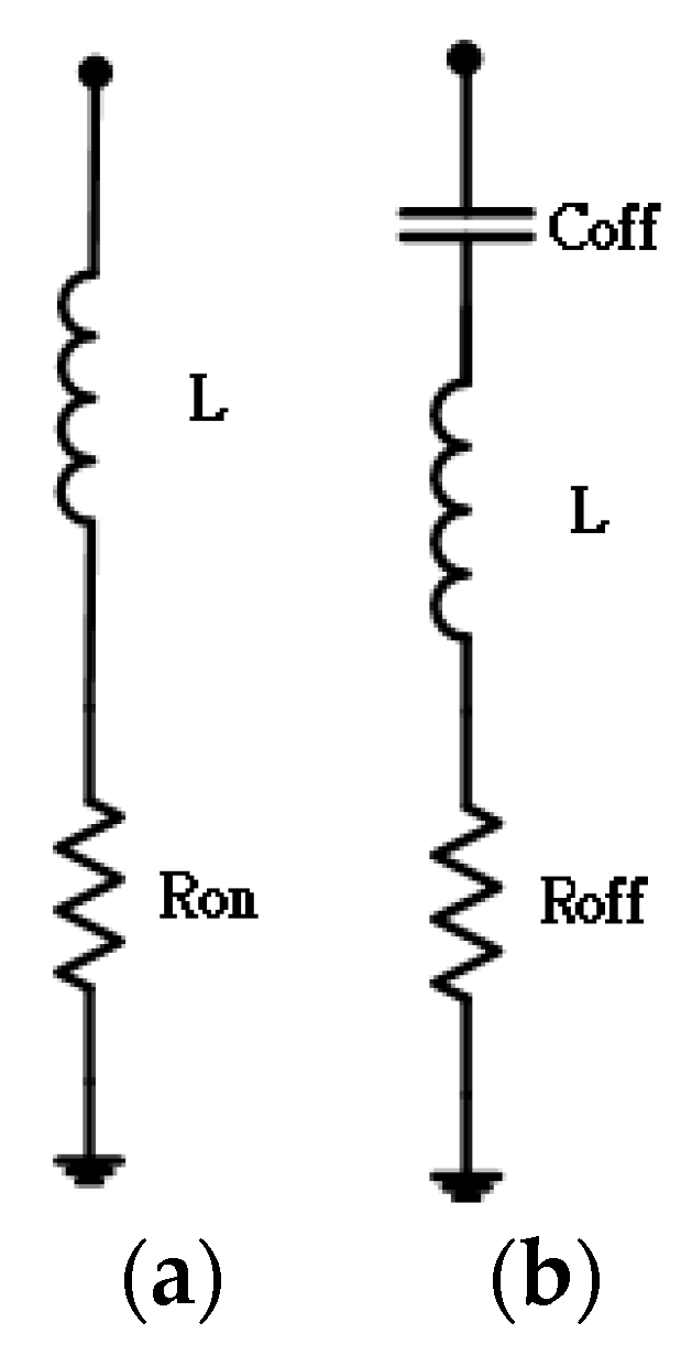
2.1. Analysis

Figure 1 shows the generic schematic of a shunt-type SPDT switch in which the devices are connected in the shunt topology. The signal path is controlled through proper gate bias of the devices connected in the shunt arms to modulate the drain-to-source impedance levels. The impedance and electric length of the transmission lines in the main arm could be optimized for the impedance match at the common port (Input, Port 1).
The basic operation mechanism of an SPDT switch relies on the different impedance between the ON and OFF states of the device so that the signal can be directed to the proper port of selection. Referring to Figure 1, in general, quarter wave-length transmission lines are inserted between the devices and the common input port. In such configurations, when the ON-state device (FET1) exhibits a short-circuited drain-to-source impedance and the OFF-state device (FET2) exhibits an open-circuited one, the signal is directed to the output port on the right (port 3). Ideally, zero insertion loss (S31) and perfect isolation (S32) could be achieved. However, such condition is never possible for practical realization using HEMT devices. Moreover, as the device peripheries becomes smaller in order to boost for operation frequencies, device parasitic effects coming from the pads and from other layout features start to have non-negligible effect on the overall performance, leading to deviations of the impedance from the ideal open- and short-circuited conditions. To understand the impact of impedance variations on the insertion loss and isolation performance, we performed simulation based on the topology shown in Figure 1 in which the impedance variations (in both magnitude and phase) were pre-defined within a certain range relative to the perfect open- and short-circuited position on the Smith Chart. The pre-defined areas on the Smith Chart for both the insertion loss and isolation were set based on possible impedance transformation, which can be found as following: for short-circuit performance the range of [0.667, 0.966] for the magnitude and [−180°, −135°], [135°, 180°] for the phase were defined; as for open-circuit performance, the impedance variations were set for the magnitude as [0.818, 0.915] and [−6°, 6°] for the phase. Note that the impedance locations on the Smith Chart for the ON- and OFF-state cases were simultaneously varied during simulation. Figure 2 shows the simulated contour for the cases of insertion loss and isolation with the device set to have a gate periphery of 200 µm, each of them is biased with an on-state gate voltage (Vg1) of 0 V and an off-state gate voltage (Vg2) of −2 V. It is clearly observed that both the insertion loss and isolation levels started to degrade as the locations of the impedance moved away from the ideal case. The ideal case was defined for the combination of sweet spots showing highest magnitude of isolation and lowest magnitude of insertion loss for the two parameters. For instance, we can observe that the ideal case for the lowest insertion loss will be around 1 ohm for open-circuit and around 75 ohm, but with such combination we can only achieve a relatively poor isolation of 24 dB comparing to the optimum isolation of roughly 35 dB, which shows an obvious difference between the sweet spots combination for isolation and insertion loss. A trade-off between the two key parameters for an SPDT switch can be expected for further design progress, as shown in Section 2.3. Meanwhile, it is also clear that the ratio between the real parts of the OFF-state to ON-state impedance determines the level of isolation. Generally, the higher the ratio is, the higher isolation level could be achieved.

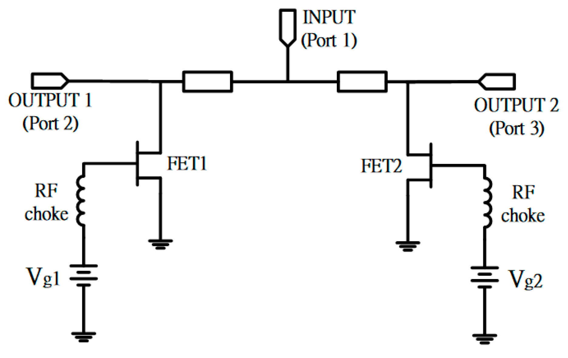
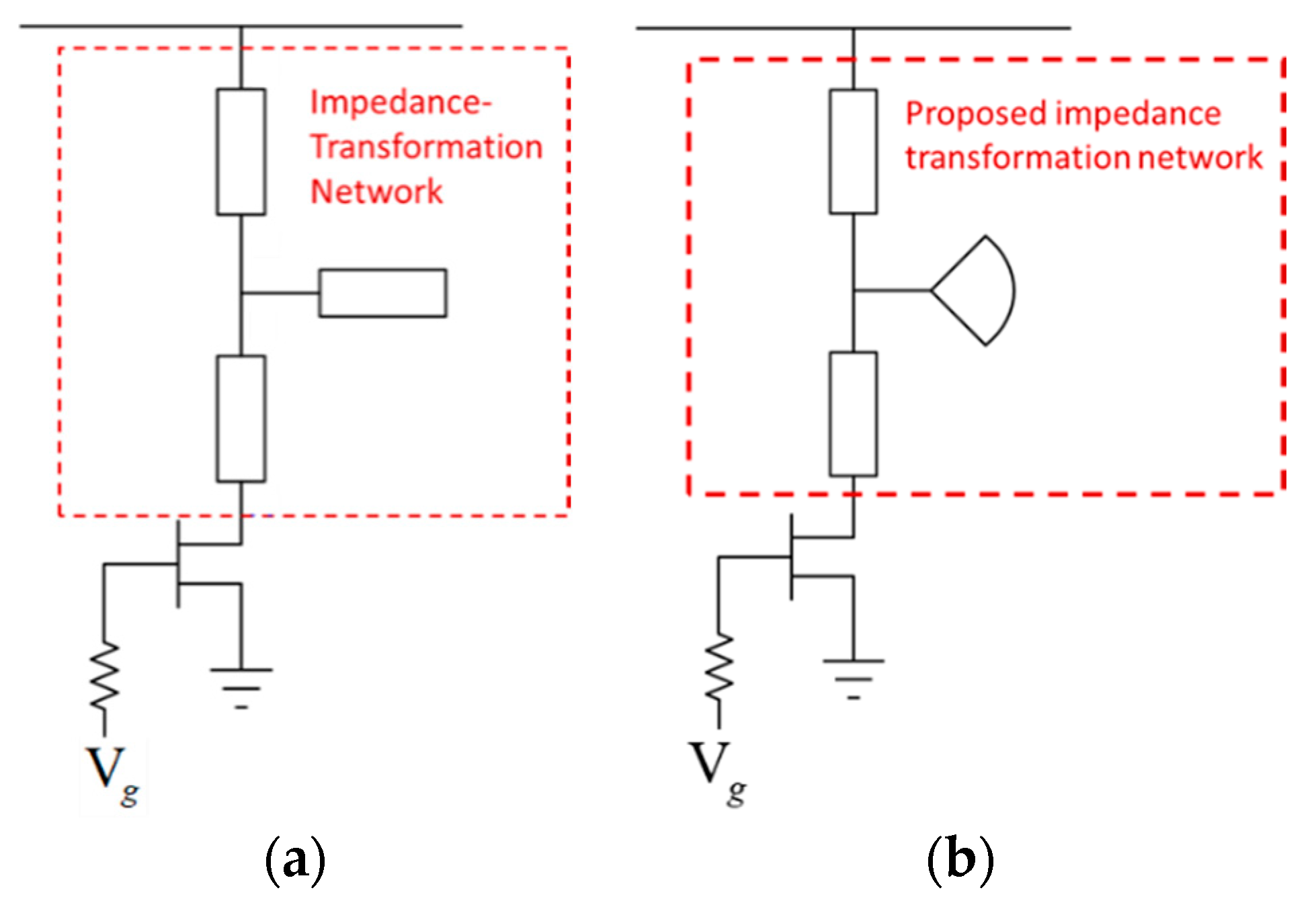
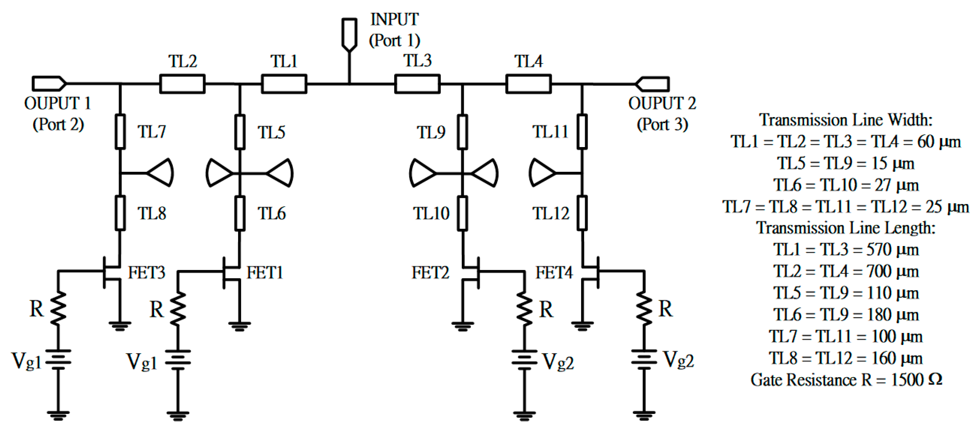
2.2. SPDT Switch With Impedance Transformation Network

The concept of incorporating the impedance transformation network in the design of shunt-type passive HEMT SPDT switch was firstly proposed in [9] for operation frequencies above Ka-band. In Figure 3, the simplified model of FET switches operating at ON- and OFF-state reported in [9] are shown. The main idea was to compensate for the highly capacitive device impedance at the OFF-state using the open-stub component such that the impedance became purely real at the desired frequency. In the meantime, the inductive nature of the device impedance at the ON-state was also compensated. While such approach solved the issue on the poor isolation of the conventional resonated HEMT configurations [11,12,13], the operation bandwidth could be limited. This is mainly due to the compensation of the imaginary parts of the impedance at ON- and OFF-states is achieved through frequency-dependent element in the impedance transformation network, namely, the open stub shown in Figure 4a. Additionally, due to the highly frequency-dependent nature of such component (since the geometry is directly related to the operating wavelength), compensation of the imaginary part of the impedance could only be effective at single frequency.
To overcome such issue, we propose a new impedance-transform network as shown in Figure 4b. In this new configuration, radial-stub element is included to replace the original open-stub one since the variation of the impedance is less frequency-dependent, which is considered as the advantage of radial-stub over the original open-stub. Figure 5 shows the comparison of the impedance for the two elements. With the impedance (both magnitude and phase) at 38 GHz set to be exactly the same, it is obvious that the radial-stub configuration shows less variation in terms of both the magnitude and phase over the frequency range of interest. Note that the simulation was performed over a frequency range from 25 GHz to 55 GHz with all the dielectric and metallic loss included.
To further investigate the effect of the radial-stub in the impedance transformation network, we followed the procedure as outlined in [9] to design the impedance transformation network based on the topology shown in Figure 4. The HEMT device used is the standard 0.15-µm pHEMT MMIC process from WIN Semiconductor. The total gate peripheries of the device used for simulation was 200 µm and the gate biases were set to be 0V for the ON-state and −2 V for the OFF-state, respectively. Figure 6 shows the trajectories of the impedance looking into specific locations of the impedance transformation network for the conventional case and the one with radial-stub. The exactly same definition in [9] was used for the analysis. Note that since the main concern is in the operation bandwidth, we swept the frequency from 25 to 55 GHz during the analysis other than just plotting the impedance at the desired frequency as was done in [9]. Meanwhile, the impedance at 38 GHz were transformed to the same spot for both cases in Figure 6 for comparison fairness. Comparing the trajectories for the transformation network with open-stub (Figure 6a) and the radial-stub (Figure 6b), it is clear that the ones for the radial-stub exhibit less angular span and magnitude variation especially at ON-state. The effect is not as pronounced at OFF-state due to high impedance seen at the drain terminal to start with.

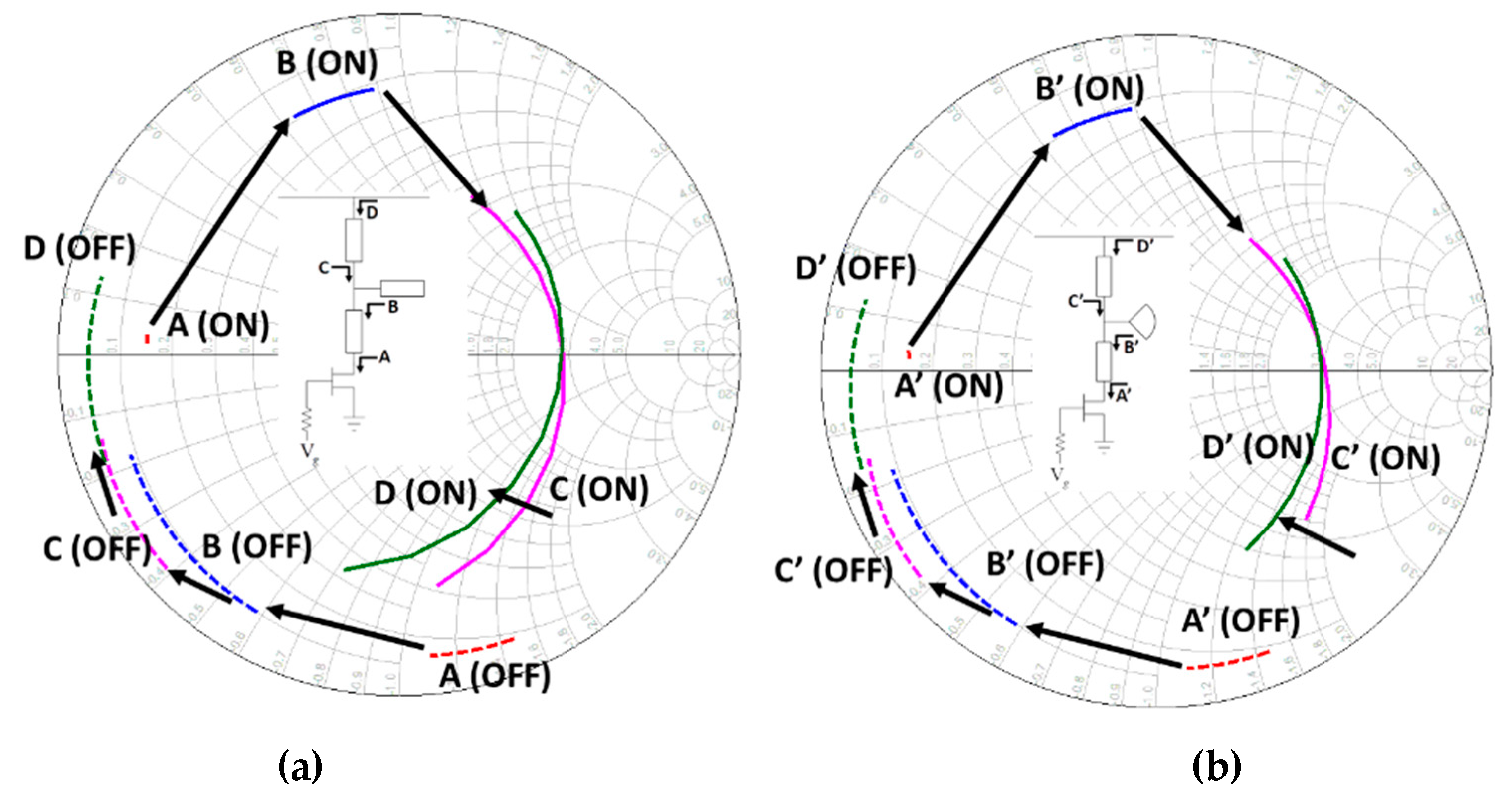
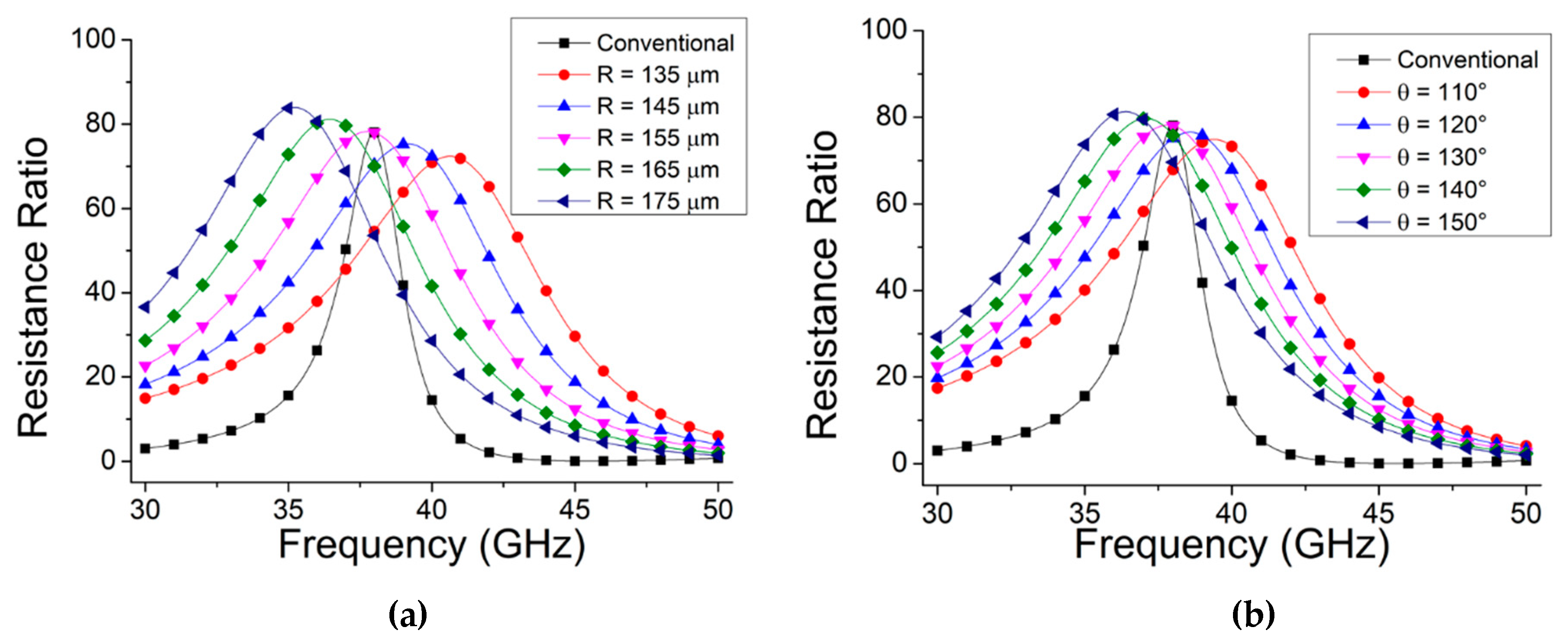
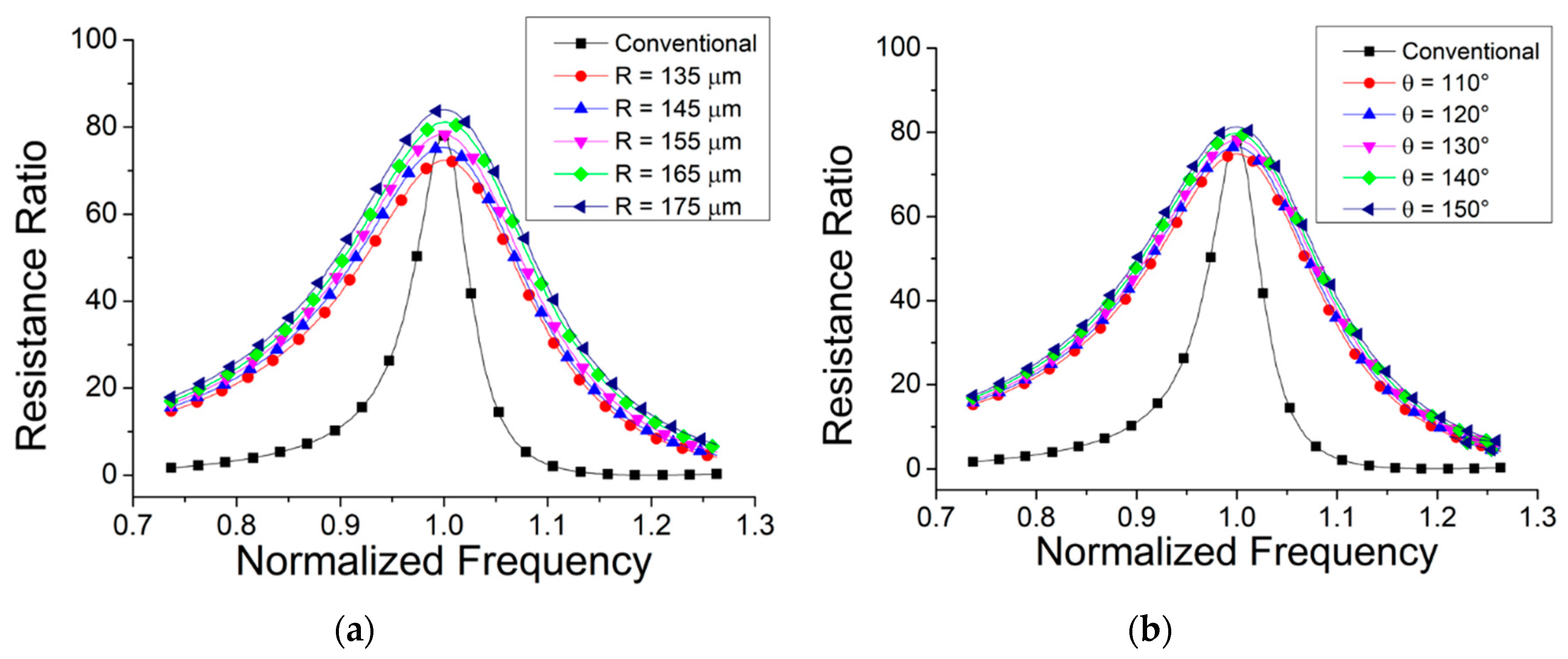
2.3. Parametric Study on the Geometry of the Radial-stub

In this section, the effect of the geometry, namely, the radius (R) and the angle of span (θ) of the radial-stub will be investigated. From the analysis results shown in Figure 2, we can conclude that the ratio of the real part of the impedance (or resistance) between the ON- and OFF-state plays a critical role in the determination of the overall switch performance. Additionally, based on the same analysis, the direct relationship between the resistance ratio and the isolation level can be obtained. Figure 7a plots the resistance ratio as a function of frequency with fixed and varying R. A similar plot for the case of fixed R and varying is shown in Figure 7b. In both plots, the peak resistance ratio corresponding to the best isolation level shifts towards low frequency as the total area of the radial stub increases, which is mainly due to the increase in the level of the capacitive loading to the impedance transformation network. The corresponding ratio for the case of conventional open stub is also included in the plots as the reference.
The effect of the radial-stub geometry on the overall bandwidth performance is presented in Figure 8 with the resistance ratio plotted as a function of the normalized frequency. As observed, compared to the conventional topology using open stub, the effective area of the overall radial stub has to exceed certain value to maintain the same (or higher) resistance ratio compared to the conventional one. It is also obvious that for the same threshold of resistance ratio, the case with radial stub exhibits a wider frequency response leading to a wider frequency bandwidth.
Finally, the effect of combination for the variations in both the radius (R) and the angular span (θ) is presented as impedance trajectories on the Smith Chart as shown in Figure 9. The frequency swept was set to be from 30 GHz to 40 GHz covering the entire band of interest. The corresponding contours of insertion loss and isolation from Figure 2 are also included on the same Smith Chart. Based on such information, the geometries of the radial stub can be uniquely synthesized with the desired level of the insertion loss and isolation specified. As a single stage approach shown in Figure 1, we had reached a level of isolation better than 25 dB and insertion loss less than 1.5 dB, where the radius of the radial stub (R) was synthesized to be 157 µm and the angular span (θ) was 129°.

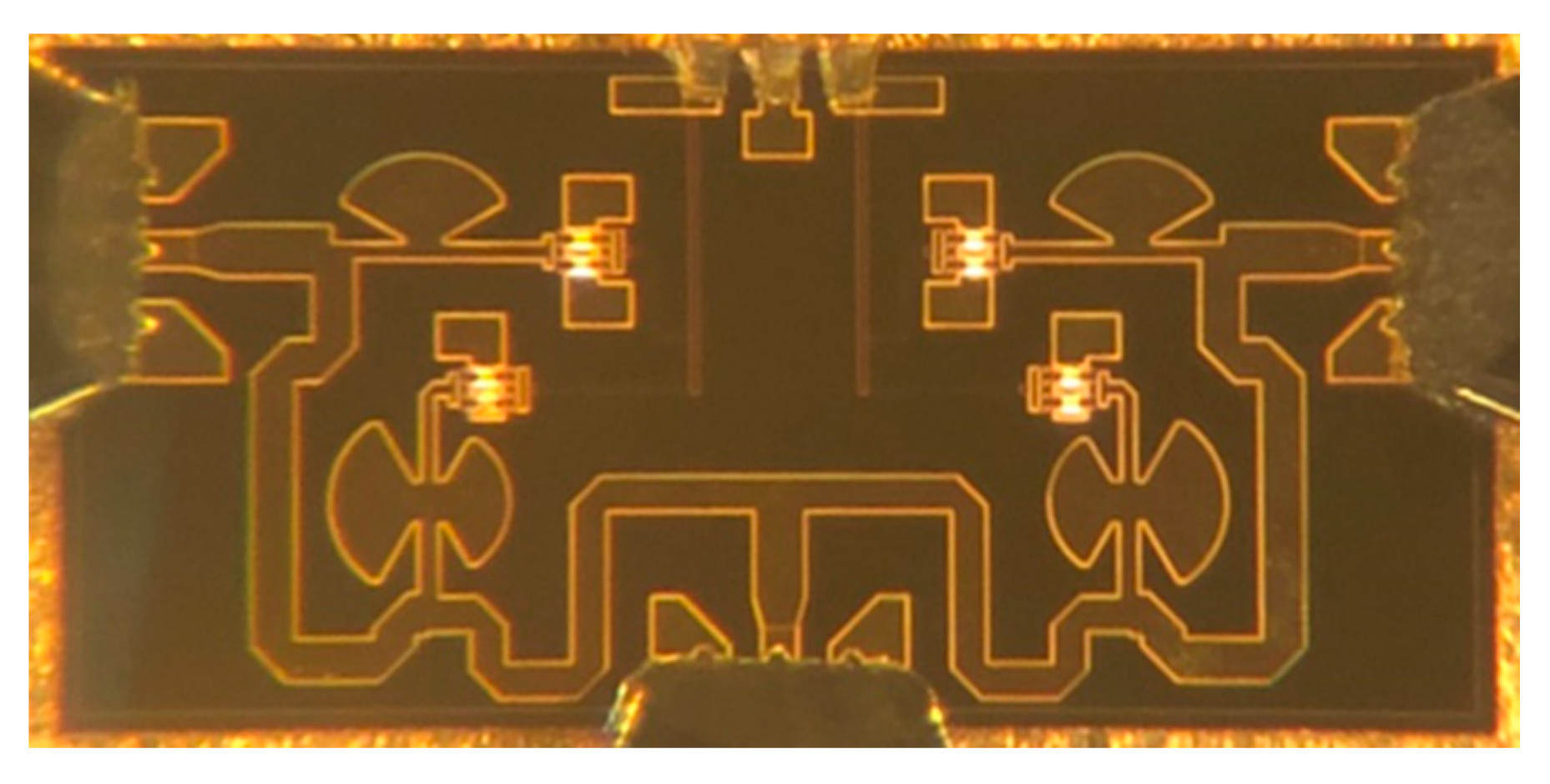
2.4. Chip Design and Implementation

For comparison purpose, the SPDT switch was designed based on the same frequency band specified in [9], namely, at Ka-band with center frequency 38 GHz. To show the effect of the radial stub in the extension of the operation bandwidth, the same number of shunt segments (which is two) as in [9] was adopted for the purpose of fairness. Figure 10 shows the complete schematic of the SPDT switch with radial stubs in the impedance transformation network. The total gate width of the device adopted was 200 µm. The chip was implemented using standard 0.15-µm pHEMT MMIC process from WIN Semiconductor, exhibiting a cutoff frequency (fT) of 70 GHz and a peak DC transconductance (Gm) of 570 mS/mm; whereas the technology used in [9] was the TRW standard 0.15-µm InGaAs/AlGaAs/GaAs pHEMT process with an fT of 70 GHz and a Gm of 580 mS/mm. Figure 11 shows the photograph of the chip. The overall dimension of the chip is 2 mm by 1 mm including the on-wafer G-S-G probing pads at all the ports and dicing street.

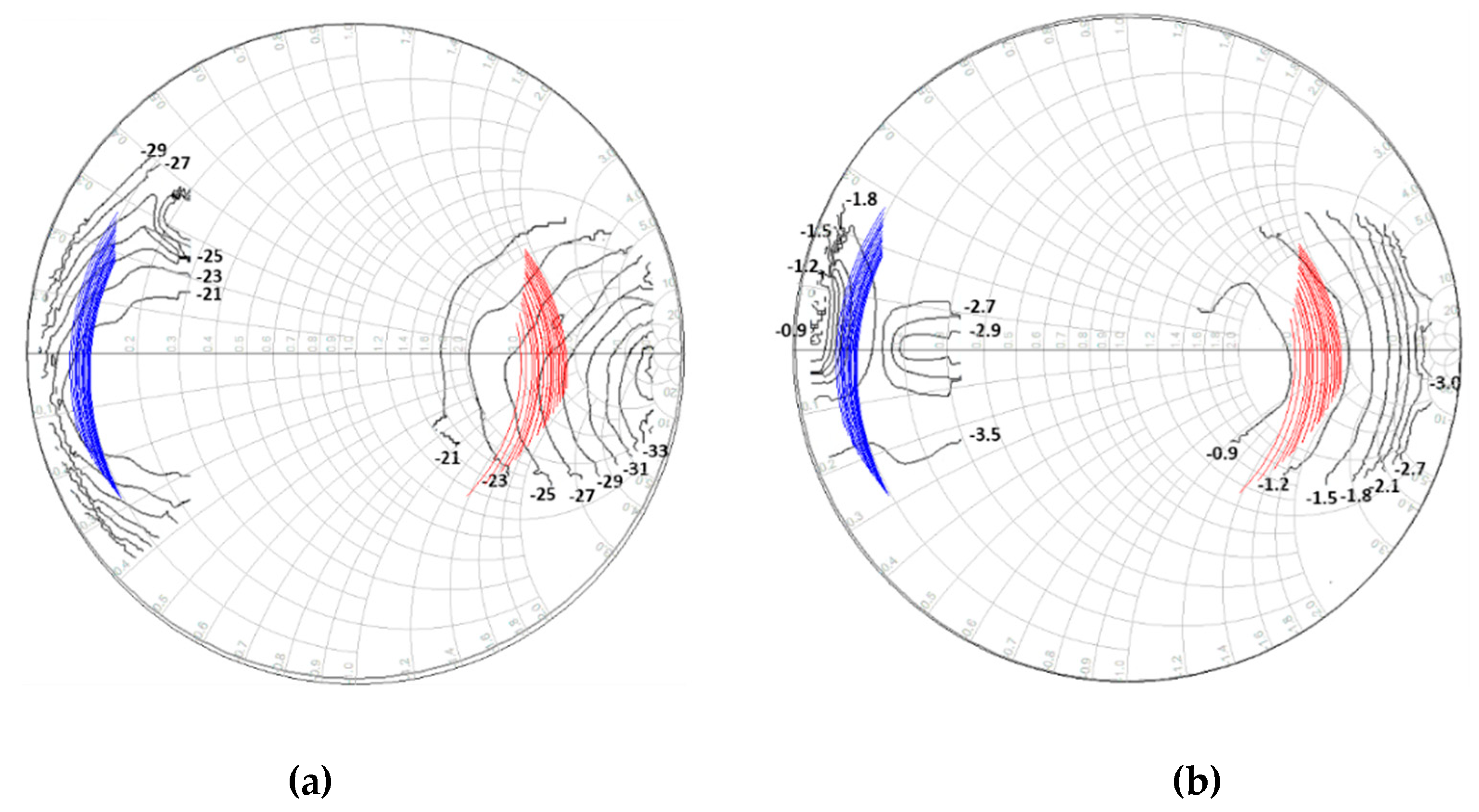
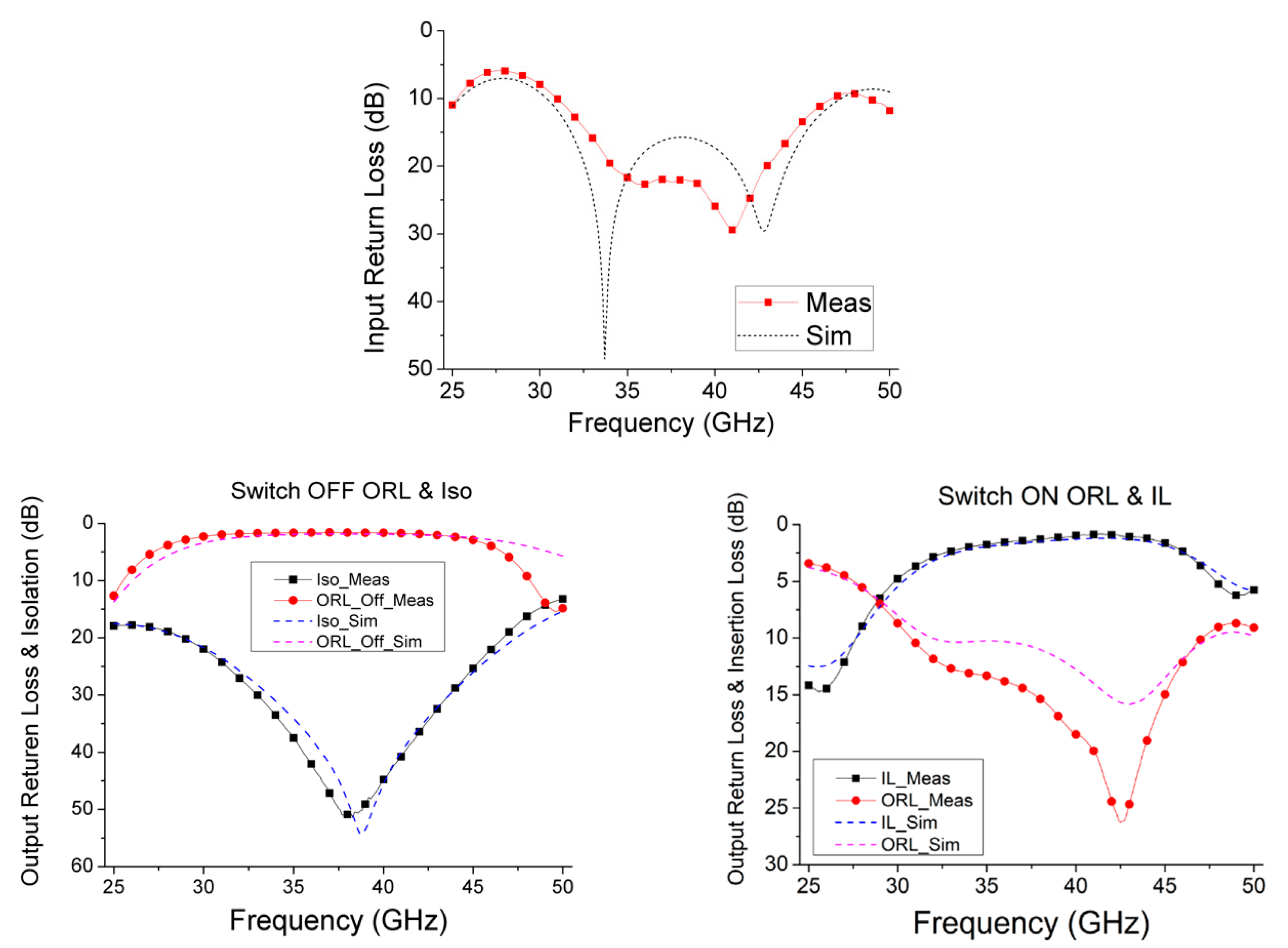
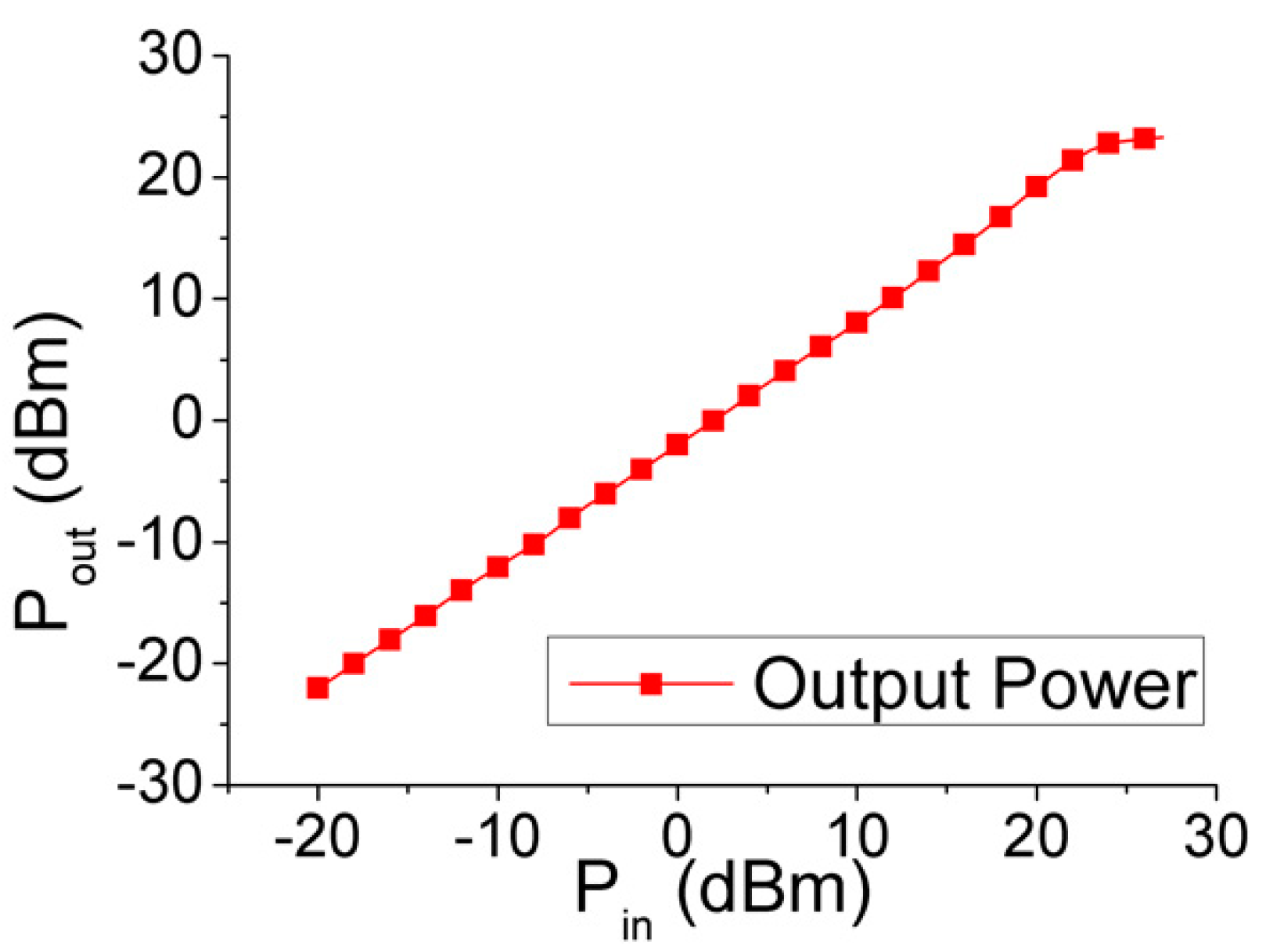
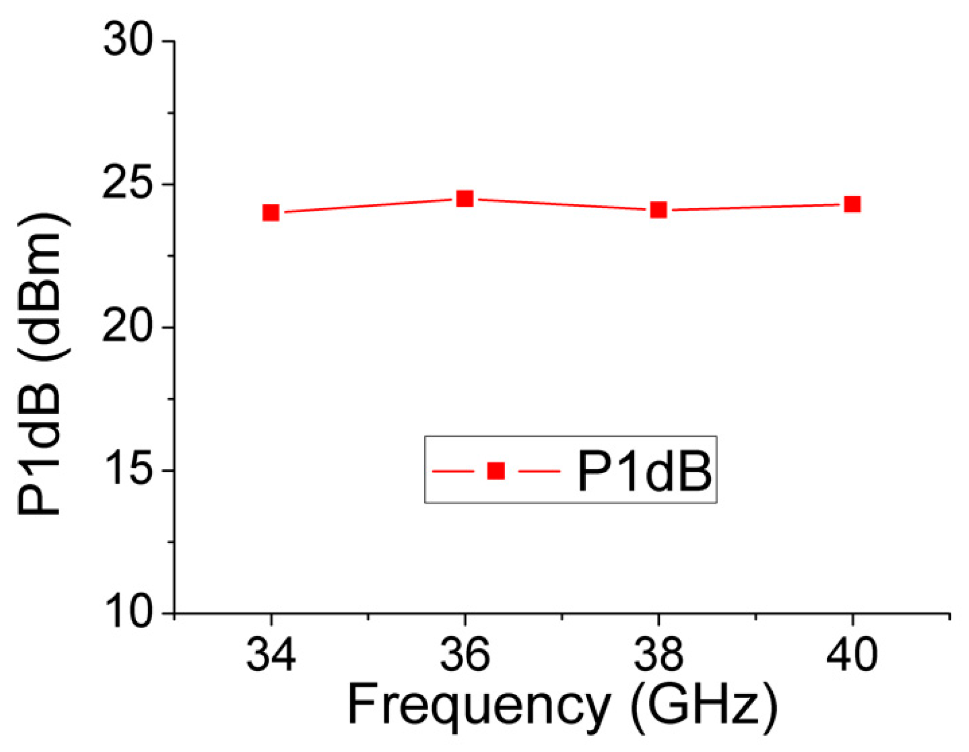
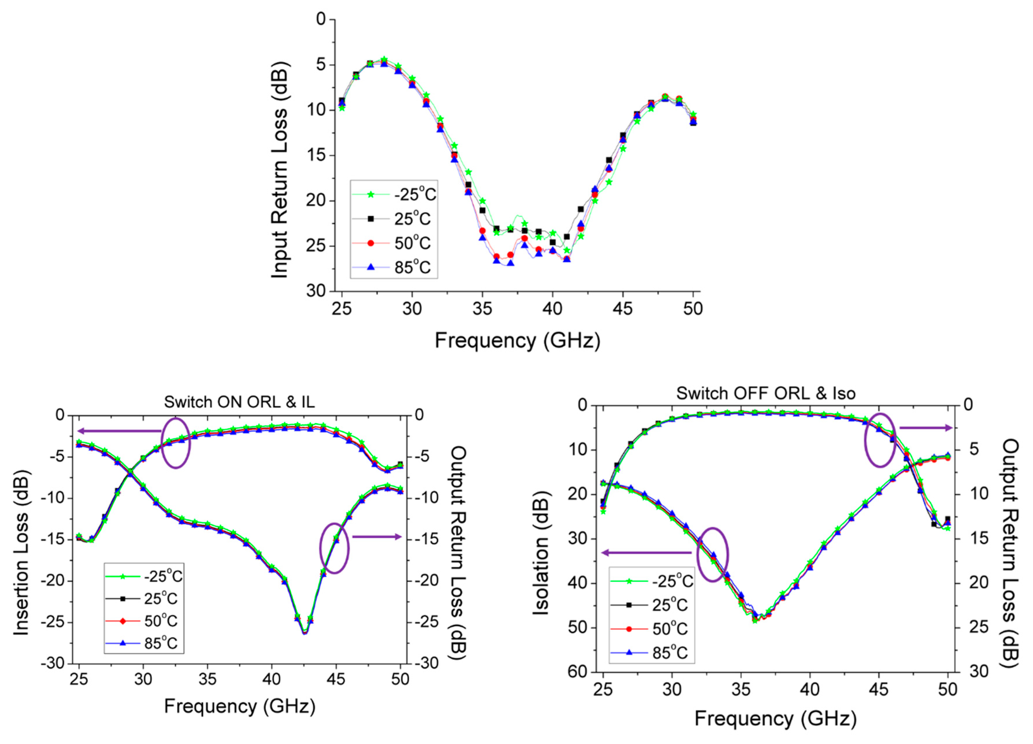
3. Measurement Results and Discussion

The fabricated SPDT MMIC switch was measured via on-wafer probing system with Agilent N5225A network analyzer up to 50 GHz. Small-signal S-parameters of each path were measured by terminating the output port of the other path. The control voltage for ON-state was set to be 0 V and that for OFF-state was −2 V, respectively. Figure 12 shows the measured input return loss at the common port, the ON-state return loss and insertion loss, and the OFF-state return loss and isolation. In all the figures, the simulated results were also included for comparison, showing good agreement with measurement ones. As observed, the SPDT switch exhibited an insertion loss of less than 2.5 dB with better than 30 dB isolation level from 33 GHz to 44 GHz, corresponding to a percent bandwidth of 28.5% centered at 38.5 GHz. The slight difference between the simulated and measured results was mainly due to the shift in the threshold voltage of the device at pinched—off condition leading to slight variations in terms of the parasitic gate capacitance for compensation.
The output power versus input power was measured to characterize the power handling capability of the fabricated SPDT MMIC switch. Figure 13 shows the measured results at 38 GHz which exhibited a 1-dB compression output power (P1dB) close to 25 dBm. Figure 14 shows the measured P1dB across the frequency band from 34 to 40 GHz, exhibiting an almost constant P1dB over the entire frequency band of interest.
To examine the temperature stability of the fabricated chip, we have also measured the corresponding performance with temperature varying from −25°C to 85°C and the results were presented in Figure 15. Clearly, very good performance stability with temperature was observed. Table 1 summarizes the performance of passive HEMT (or FET) switches at millimeter-wave frequencies from previously published works. Compared to previous publications, the proposed topology exhibited a substantial improvement in terms of the operation bandwidth.

4. Conclusions

In this paper, a new configuration of MMIC SPDT passive HEMT switches targeted for operation at millimeter frequencies was proposed. With the radial-stub component included in the impedance transformation network, substantial improvement in the operation bandwidth has been achieved. The measurement results of the MMIC chip implemented in the standard 0.15-µm GaAs pHEMT technology demonstrated a very wide operation bandwidth from 33 GHz to 44 GHz with better than 30 dB isolation and good insertion loss. Extension of such design concept and methodology is possible to cover the complete operation bandwidth for fifth-generation (5G) communication system at millimeter-wave frequencies.

Author Contributions

Conceptualization and methodology, H.-T.H., J.W. and Y.-F.T.; software and validation, Y.-F.T.; writing—original draft preparation, Y.-F.T.; writing—review and editing, H.-T.H., J.W. and Y.-F.T.; supervision, project administration and funding acquisition, H.-T.H. All authors have read and agreed to the published version of the manuscript.

Funding

This research was funded by the Ministry of Science and Technology, Taiwan, under Grants 107-2221-E-009-093-MY2 and 108-2911-I-009-502. This research was also financially supported by the “Center for the Semiconductor Technology Research” from The Featured Areas Research Center Program within the framework of the Higher Education Sprout Project by the Ministry of Education (MOE) in Taiwan and also funded in part by the Ministry of Science and Technology, Taiwan, under Grant MOST-108-3017-F-009-003.

Acknowledgments

The authors gratefully acknowledge the fabrication and measurement of the chip through Taiwan Semiconductor Research Institute (TSRI).

Conflicts of Interest

The authors declare no conflict of interest.

References

  1. Shigematsu, T.; Suematsu, N.; Takeuchi, N.; Iyama, Y.; Mizobuchi, A. A 6-18 GHz 20 W SPDT switch using shunt discrete PIN diodes. In Proceedings of the 1997 IEEE MTT-S International Microwave Symposium Digest, Denver, CO, USA, 8–13 June 1997; Volume 2, pp. 527–530. [Google Scholar]
  2. Rozbicki, A.; Brogle, J.; Jain, N.; Boles, T.; Hoag, D. Ka band high power AlGaAs PIN diode switches. In Proceedings of the 2009 IEEE MTT-S International Microwave Symposium Digest, Boston, MA, USA, 7–12 June 2009; pp. 453–456. [Google Scholar]
  3. Yang, J.G.; Yang, K. High-Linearity K-Band Absorptive-Type MMIC Switch Using GaN PIN-Diodes. IEEE Microw. Wirel. Compon. Lett. 2013, 23, 37–39. [Google Scholar] [CrossRef]
  4. Gong, Y.; Teng, J.W.; Cressler, J.D. A Compact, High-Power, 60 GHz SPDT Switch Using Shunt-Series SiGe PIN Diodes. In Proceedings of the 2019 IEEE Radio Frequency Integrated Circuits Symposium (RFIC), Boston, MA, USA, 2–4 June 2019; pp. 15–18. [Google Scholar]
  5. Zhao, L.; Liang, W.-F.; Zhou, J.-Y.; Jiang, X. Compact 35–70 GHz SPDT Switch with High Isolation for High Power Application. IEEE Microw. Wirel. Compon. Lett. 2017, 27, 485–487. [Google Scholar] [CrossRef]
  6. Zheng, X.; Tremblay, J.C.; Huettner, S.E.; Ip, K.P.; Papale, T.; Lange, K.L. Ka-Band High Power GaN SPDT Switch MMIC. In Proceedings of the 2013 IEEE Compound Semiconductor Integrated Circuit Symposium (CSICS), Monterey, CA, USA, 13–16 October 2013; pp. 1–5. [Google Scholar]
  7. Thian, M.; Fusco, V.F. Ultrafast Low-Loss 42–70 GHz Differential SPDT Switch in 0.35 µm SiGe Technology. IEEE Trans. Microw. Theory Tech. 2012, 60, 655–659. [Google Scholar] [CrossRef]
  8. Uzunkol, M.; Rebeiz, G. A Low-Loss 50–70 GHz SPDT Switch in 90 nm CMOS. IEEE J. Solid State Circuits 2010, 45, 2003–2007. [Google Scholar] [CrossRef]
  9. Lin, K.-Y.; Wang, Y.-J.; Niu, D.-C.; Wang, H. Millimeter-wave MMIC single-pole-double-throw passive HEMT switches using impedance-transformation networks. IEEE Trans. Microw. Theory Tech. 2003, 51, 1076–1085. [Google Scholar] [CrossRef]
  10. Shairi, N.A.; Ahmad, B.H.; Wong, P.W. SPDT discrete switch design using switchable radial stub resonator for WiMAX and LTE in 3.5 GHz band. In Proceedings of the 2013 IEEE International RF and Microwave Conference (RFM), Penang, Malaysia, 9–11 December 2013; pp. 1–5. [Google Scholar]
  11. Madihian, M.; Desclos, L.; Maruhashi, K.; Onda, K.; Kuzuhara, M. A sub-nanosecond resonant-type monolithic T/R switch for millimeter-wave systems applications. IEEE Trans. Microw. Theory Tech. 1998, 46, 1016–1019. [Google Scholar] [CrossRef]
  12. Lan, G.L.; Dunn, D.L.; Chen, J.C.; Pao, C.K.; Wang, D.C. A high performance V-band monolithic FET transmit-receive switch. In Proceedings of the IEEE 1988 Microwave and Millimeter-Wave Monolithic Circuits Symposium Digest of Papers, New York, NY, USA, 24–25 May 1998; pp. 99–101. [Google Scholar]
  13. Aust, M.; Wang, H.; Carandang, R.; Tan, K.; Chen, C.H.; Trinh, T.; Esfandiari, R.; Yen, H.C. GaAs monolithic components development for Q-band phased array application. In Proceedings of the 1992 IEEE Microwave Symposium Digest MTT-S, Albuquerque, NM, USA, 1–5 June 1992; Volume 2, pp. 703–706. [Google Scholar]
  14. Schindler, M.J.; Morris, A. DC–40 GHz and 20–40 GHz MMIC SPDT switches. IEEE Trans. Microw. Theory Tech. 1987, 35, 1486–1493. [Google Scholar] [CrossRef]
  15. Ingram, D.L.; Cha, K.; Hubbard, K.; Lai, R. Q-band high isolation GaAs HEMT switches. In Proceedings of the GaAs IC Symposium IEEE Gallium Arsenide Integrated Circuit Symposium. 18th Annual Technical Digest 1996, Orlando, FL, USA, 3–6 November 1996; pp. 289–292. [Google Scholar]
  16. Mizutani, H.; Funabashi, N.; Kuzuhara, M.; Takayama, Y. Compact DC–60-GHz HJFET MMIC switches using OHMIC electrode-sharing technology. IEEE Trans. Microw. Theory Tech. 1998, 46, 1597–1603. [Google Scholar] [CrossRef]
  17. Hieda, M.; Nakahara, K.; Miyaguchi, K.; Kurusu, H.; Iyama, Y.; Takagi, T.; Urasaki, S. High-isolation series-shunt FET SPDT switch with a capacitor canceling FET parasitic inductance. IEEE Trans. Microw. Theory Tech. 2001, 49, 2453–2458. [Google Scholar] [CrossRef]
  18. Zhang, L.; Cheng, X.; Deng, X.; Li, X. Design of K/Ka-band passive HEMT SPDT switches with high isolation. In Proceedings of the 2017 China Semiconductor Technology International Conference (CSTIC), Shanghai, China, 12–13 March 2017; pp. 1–3. [Google Scholar]
  19. Trinh, K.T.; Kao, H.-L.; Chiu, H.-C.; Karmakar, N.C. A Ka-Band GaAs MMIC Traveling-Wave Switch With Absorptive Characteristic. IEEE Microw. Wirel. Compon. Lett. 2019, 29, 394–396. [Google Scholar] [CrossRef]
Figure 1. Schematic of the generic of a shunt-type single-pole-double-throw (SPDT) switch.
Electronics 09 00270 g001
Figure 2. Simulated impedance contour based on the generic topology shown in Figure 1: (a) Insertion loss contour; (b) Isolation contour. (Both in unit of dB)
Electronics 09 00270 g002
Figure 3. The simplified small signal model of FET switches.: (a) ON-state model; (b) OFF-state model.
Electronics 09 00270 g003
Figure 4. Topology of the impedance transformation network.: (a) conventional configuration with open-stub element; (b) proposed one with radial-stub element.
Electronics 09 00270 g004
Figure 5. Comparison of impedance variation between an open-stub and radial-stub.
Electronics 09 00270 g005
Figure 6. Trajectories of the impedance transform based on different topologies: (a) Conventional topology using open-stub element; (b) Proposed one using radial-stub element. (Dashed lines represent the impedance of OFF-state; Solid lines for the impedance of ON-state.).
Electronics 09 00270 g006
Figure 7. The resistance ratio as functions of frequency for the cases of (a) fixed θ of 130° with varying R; and (b) fixed R of 155 µm with varying. The same ratio for the conventional topology using open stub is also included in the plots.
Electronics 09 00270 g007
Figure 8. The resistance ratio as functions of normalized frequency for the cases of (a) fixed θ of 130o with varying R; and (b) fixed R of 155 µm varying θ. The same ratio for the conventional topology using open stub is also included in the plots.
Electronics 09 00270 g008
Figure 9. The effect of combination for the variations in both the radius (R) and the angular span (θ) presented as impedance trajectories on the Smith Chart with corresponding performance contours of (a) the insertion loss, and (b) the isolation level for frequency ranging from 30 GHz to 40 GHz.
Electronics 09 00270 g009
Figure 10. The complete schematic of the proposed SPDT switch with radial stub implemented in the impedance transform network.
Electronics 09 00270 g010
Figure 11. Chip photograph of the fabricated SPDT switch in standard 0.15-µm pHEMT MMIC process from WIN Semiconductor.
Electronics 09 00270 g011
Figure 12. Measured small-signal performance of the fabricated chip with simulation results included.
Electronics 09 00270 g012
Figure 13. Measured output power versus input power of the SPDT switch at 38 GHz.
Electronics 09 00270 g013
Figure 14. Measured P1dB across the frequency band of interest of the SPDT switch.
Electronics 09 00270 g014
Figure 15. Measured small-signal performance of the fabricated chip with varying temperature.
Electronics 09 00270 g015
Table 1. Comparison of performance between proposed design and previous published works.
Ref.Tech.StructureFreq. (GHz)Input Return Loss (dB)Insertion Loss (dB)Isolation (dB)P1dB
(dBm)
Chip Size
(mm2)
[5]0.1-μm GaAs pHEMTDistributed 6 shunt stacked HEMTs35–70> 15< 3> 4020.2 @ 31GHz0.96
[9]0.15-μm GaAs pHEMTShunt with impedance transform network38–43> 15< 2> 30N/A2
[14]GaAsShunt configuration20–40> 72 @
40 GHz
25-28N/A1.61
[15]GaAs HEMTShunt with Quarter-wavelength42–46> 12< 1.6> 35N/A10
[16]HJFETSeries resonant and shuntDC-40N/A< 3.5> 25210.55
[17]GaAs FETSeries-shunt configuration2812.53.128.9N/A2.18
[18]0.07-μm GaAsShunt configuration24–27> 17.5< 1.5> 39N/A< 3
[19]0.15-μm GaAsTraveling-wave concept36–38> 8.1< 3.2> 2812 @ 37 GHz1.1
This Work0.15-μm GaAs pHEMTImpedance transform network with radial stub33–44> 16< 2.5> 30> 242

