Article

Polymorphic Memory: A Hybrid Approach for Utilizing On-Chip Memory in Manycore Systems

1
Division of Computer Engineering, Hankuk University of Foreign Studies, Yongin 17035, Korea
2
Samsung Electronics, Suwon 16677, Korea
3
Department of Computer and Information Security, Sejong University, Seoul 05006, Korea
*
Authors to whom correspondence should be addressed.
Electronics 2020, 9(12), 2061; https://doi.org/10.3390/electronics9122061
Submission received: 20 October 2020 / Revised: 14 November 2020 / Accepted: 26 November 2020 / Published: 3 December 2020
(This article belongs to the Special Issue Storage Systems with Non-volatile Memory Devices)

Abstract

:
The key challenges of manycore systems are the large amount of memory and high bandwidth required to run many applications. Three-dimesnional integrated on-chip memory is a promising candidate for addressing these challenges. The advent of on-chip memory has provided new opportunities to rethink traditional memory hierarchies and their management. In this study, we propose a polymorphic memory as a hybrid approach when using on-chip memory. In contrast to previous studies, we use the on-chip memory as both a main memory (called M1 memory) and a Dynamic Random Access Memory (DRAM) cache (called M2 cache). The main memory consists of M1 memory and a conventional DRAM memory called M2 memory. To achieve high performance when running many applications on this memory architecture, we propose management techniques for the main memory with M1 and M2 memories and for polymorphic memory with dynamic memory allocations for many applications in a manycore system. The first technique is to move frequently accessed pages to M1 memory via hardware monitoring in a memory controller. The second is M1 memory partitioning to mitigate contention problems among many processes. Finally, we propose a method to use M2 cache between a conventional last-level cache and M2 memory, and we determine the best cache size for improving the performance with polymorphic memory. The proposed schemes are evaluated with the SPEC CPU2006 benchmark, and the experimental results show that the proposed approaches can improve the performance under various workloads of the benchmark. The performance evaluation confirms that the average performance improvement of polymorphic memory is 21.7%, with 0.026 standard deviation for the normalized results, compared to the previous method of using on-chip memory as a last-level cache.

1. Introduction

Owing to the recent emergence of manycore systems in computing architecture, it is possible to simultaneously run many applications such as rich multimedia and scientific calculations [1,2,3,4]. Manycore systems are specialized multi-core processor-based systems designed for high-level parallel processing of data-intensive applications. The key challenge for manycore systems is how to utilize a large amount of memory with high bandwidth because most applications require a large amount of main memory [5,6,7,8,9]. However, memory latency and bandwidth are limiting factors for manycore systems. Moreover, adding more memory channels to increase the bandwidth is not an effective approach because of the pin limitation of the processor. This problem is called the “memory wall” [10].
Three-dimensional stacked on-chip Dynamic Random Access Memory (DRAM) [11,12,13,14,15] is a promising candidate for overcoming the memory wall between the processor and the memory. Placing it near the processor can significantly increase the memory bandwidth. In particular, placing it near the processor core results in lower latency compared to off-chip DRAM memory, and it is not limited by the pins of the processor. With 3D stacked on-chip memory, the computing system is organized by two types of memories: on-chip memory and conventional off-chip DRAM memory. We refer to 3D stacked on-chip memory as “M1” and off-chip DRAM memory as “M2”.
Many studies have investigated 3D stacked on-chip memory. These studies are categorized into two types: those that use on-chip memory as the last-level cache of off-chip memory [16,17,18,19,20] and those that use a flat address region with hybrid on-chip and off-chip memories [21,22,23,24,25,26]. Recently, some studies have investigated memory systems using a combination of cache and migration [27]. The relationship between M1 and M2 is (i) copying and caching data from M2 to M1 if the on-chip M1 memory is used as a DRAM cache and (ii) migration between M1 and M2 if M1 memory is used as a flat address space. The use as a cache or flat address region for on-chip memory has advantages and disadvantages. Caching sacrifices the address region; however, there is less data transfer overhead since it has no data swapping between M1 and M2. On the other hand, flat addressing does not sacrifice address space, but there is data swapping overhead between the two. It could be efficient to use a hybrid approach by achieving a suitable trade-off between the two approaches [27]. Moreover, when running multiple applications in a multi-core system, allocating the on-chip M1 memory to each application is an important issue in terms of improving the performance of the overall system [5,8,28,29,30]. However, not many existing studies have used M1 memory as a hybrid memory with a cache and flat address region; furthermore, little studies have investigated dynamic M1 allocation for manycore systems.
To achieve high performance when running numerous applications on a manycore system with a hybrid memory architecture, we designed a hybrid memory management scheme called p o l y m o r p h i c m e m o r y , in which M1 is dynamically allocated according to the state of the application running in the manycore system, and the allocated M1 is further divided into the DRAM cache and flat address region. Specifically, we designed several schemes to deal with the hybrid polymorphic memory architecture in a manycore system. The first scheme is migration between M1 and M2 for a flat address region of the memory to enhance the memory throughput by placing frequently accessed data in high-bandwidth M1 via hardware monitoring in a memory controller. For efficient migration, we proposed a monitoring method to monitor the page access pattern and to calculate the overhead of page migration. Second, in the polymorphic memory system, part of M1 is used for M2 cache to reduce the latency of memory access; we determined the best cache size for improving the performance of the polymorphic memory system. Finally, we designed an M1 partitioning scheme to mitigate contention problems and to improve the balancing of M1 allocation among many processes, which can enhance the overall throughput of the entire manycore system. Our experimental results showed that the proposed approaches can improve the performance of processes under various workloads.
The remainder of this paper is organized as follows. Section 2 reviews previous studies. Section 3 describes the management of the proposed polymorphic memory system. Section 4 presents the evaluation results. Finally, Section 5 concludes the paper and briefly explores directions for future work.

2. Related Works

Owing to the emergence of the manycore architecture after the multi-core architecture, the memory subsystem has gained a more important role in running many threads concurrently. However, the International Technology Roadmap for Semiconductors (ITRS) has reported that the pin count of a socket limits the enhancement of the memory subsystem. Thus, the capacity gap between supply and demand increases. There are two design approaches for utilizing on-chip DRAM memory: one is to use it as a DRAM cache, and the other is to deal with it as a part of the memory. Recently, some studies have combined caching and a part of memory with on-chip memory.
The DRAM cache of on-chip memory is located between the last-level Static Raneom Access Memory(SRAM) cache and the DRAM main memory. Although the latency of DRAM is somewhat greater than that of SRAM, previous studies [31,32,33] have shown that DRAM-based caches can provide twice the bandwidth of the main memory with one-third of the memory latency. The overhead of a tag array increases with the size of on-chip memory. To decrease the tag overhead, it is possible to use large cache line sizes such as 4 KB or 8 KB. However, this approach requires a high memory bandwidth because a large amount of data should be transferred in one cache miss. Zhang et al. [32] increased the DRAM cache line size to reduce the cache tag overhead. They also proposed a prediction technique that accurately predicts the hit/miss status of an access to the cached DRAM, thereby reducing the access latency. Jiang et al. [34] proposed Caching HOt Pages (CHOP) and solved the problem of a large cache line that requires a high-memory bandwidth. To this end, the authors proposed a filter-based DRAM caching technique. The filter module selects the hot pages, and these hot pages are only selected to be allocated to the DRAM cache. Woo et al. [35] proposed SMART-3D to improve the bandwidth of the DRAM cache directly.
Another drawback of using a DRAM cache is the tag checking overhead. Because the cache tags should be read to check a hit or miss at every memory request, the total latency increases. To reduce the hit latency, Loh et al. [16] scheduled the tag and data accesses as a composite access and proposed a new DRAM cache design to ensure that data access is always a row buffer hit. The row buffer size is 2 KB, and it is divided into 32 blocks of 64 bytes. The authors developed a set-associative DRAM cache with 64-byte cache lines. Further, they designed MissMap to manage a vector of block-valid bits for the pages, which is stored in the L2 SRAM cache. We refer to it as LH-Cache. Qureshi et al. [17] introduced Alloy Cache, which is a direct-mapped cache [36]. They tightly integrated tags and data into a single entity called TAD (tag and data); TAD can be read at one memory access with a direct-mapped cache. Furthermore, they designed a parallel access model (PAM) in which DRAM cache and DRAM memory accesses are performed in parallel. PAM is used along with the memory access predictor when the hit ratio on Alloy Cache is low. However, if the hit ratio is high, most accesses to DRAM memory are unnecessary; thus, PAM requires a high memory bandwidth. Other studies have attempted to reduce the tag access latency by locating tags on the processor die. Huang designed a small SRAM cache for a DRAM cache tag to reduce the tag lookup latency [18], while Vasilakis et al. organized the tags of on-chip Last-Level Cache (LLC) for storing tag information of the DRAM cache [19]. Yu et al. used Translation Lookaside Buffers (TLBs) to track the contents of the DRAM cache and designed a bandwidth-aware replacement policy for balanced use of the DRAM cache and main memory [20].
As another approach, on-chip DRAM can be used as a part of the main memory of the system. In this case, both a conventional DRAM such as DDR3 and on-chip DRAM are organized as the main memory. Existing Operating Systems (OSs) can operate in this manner without modification; however, the OS should be able to manage two types of memories with knowledge of their distinct features such as latencies and bandwidths to achieve high performance. In the memory scheme, data migration occurs between on-chip memory and off-chip memory, and the main decision factors are the migration granularity, flexibility, and how to select data to be migrated.
Furthermore, in the memory scheme, migration data can be selected with some hardware support, or the OS can select the data to be migrated without the aid of hardware. Dong et al. [21] focused on how to reduce the migration overhead and proposed data migration between on-chip and off-chip memory, in which the unit of migration is a macro page; the macro page size ranged from 4 KB to 4 MB. Chou et al. [22] divided the memory into several memory groups, and migration is only performed in a group that reduced the remapping overhead. Sim [23] deployed hardware competing counters in a segment group and used a threshold value for dynamic adjustment. Cemelon [24] created new instructions for allocation and migration of data in group-based hybrid memory. Mempod [25] attempted to overcome group-based migration and performed all-to-all migration using the majority element algorithm. Vasilakis [26] proposed an LLC-guided data migration scheme for hybrid memory systems and subsequently combined caching and migration [27], in which some small parts of on-chip memory were used for caching. Their metadata were supported by a common mechanism to alleviate the overhead. However, this approach does not consider the manycore architecture for allocating on-chip memory.
Therefore, nowadays, many existing approaches that use 3D stacked on-chip DRAM memory are evolving toward hybrid memory systems that use a combination of a cache and a part of memory. Moreover, a dynamic memory partition and allocation method for on-chip DRAM memory is required to efficiently run multiple data-intensive applications in a manycore system. Our polymorphic memory system is designed as a hybrid memory that uses on-chip memory as both a DRAM cache and a part of memory, and the dynamic partitioning method of on-chip M1 memory between processes solves the contention problem of multiple processes in manycore systems.

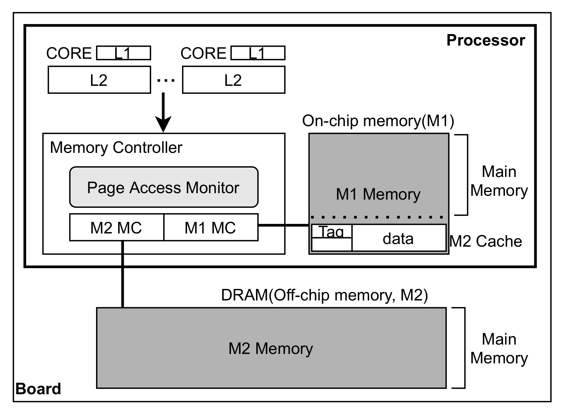
3. Polymorphic Memory System

In the polymorphic memory system, the main memory consists of M1 memory and M2 memory; M1 is placed in the processor and shows higher bandwidth and lower latency than M2 memory. The architecture of polymorphic memory system is described in Figure 1. We assume that the main memory is exclusively arranged through the physical memory area and physically divided by the memory address space. We also use some parts of M1 as a DRAM cache of M2 to take advantage of both a cache and a memory with the low latency of M1. In addition, in a multi-process and manycore environment, many processes attempt to obtain a larger amount of M1 memory to execute their tasks more rapidly, i.e., they can contend for large M1 memory. Distinct memory management is needed to allocate frequently accessed pages into M1 memory and to solve the contention problem among multiple processes to improve overall performance.

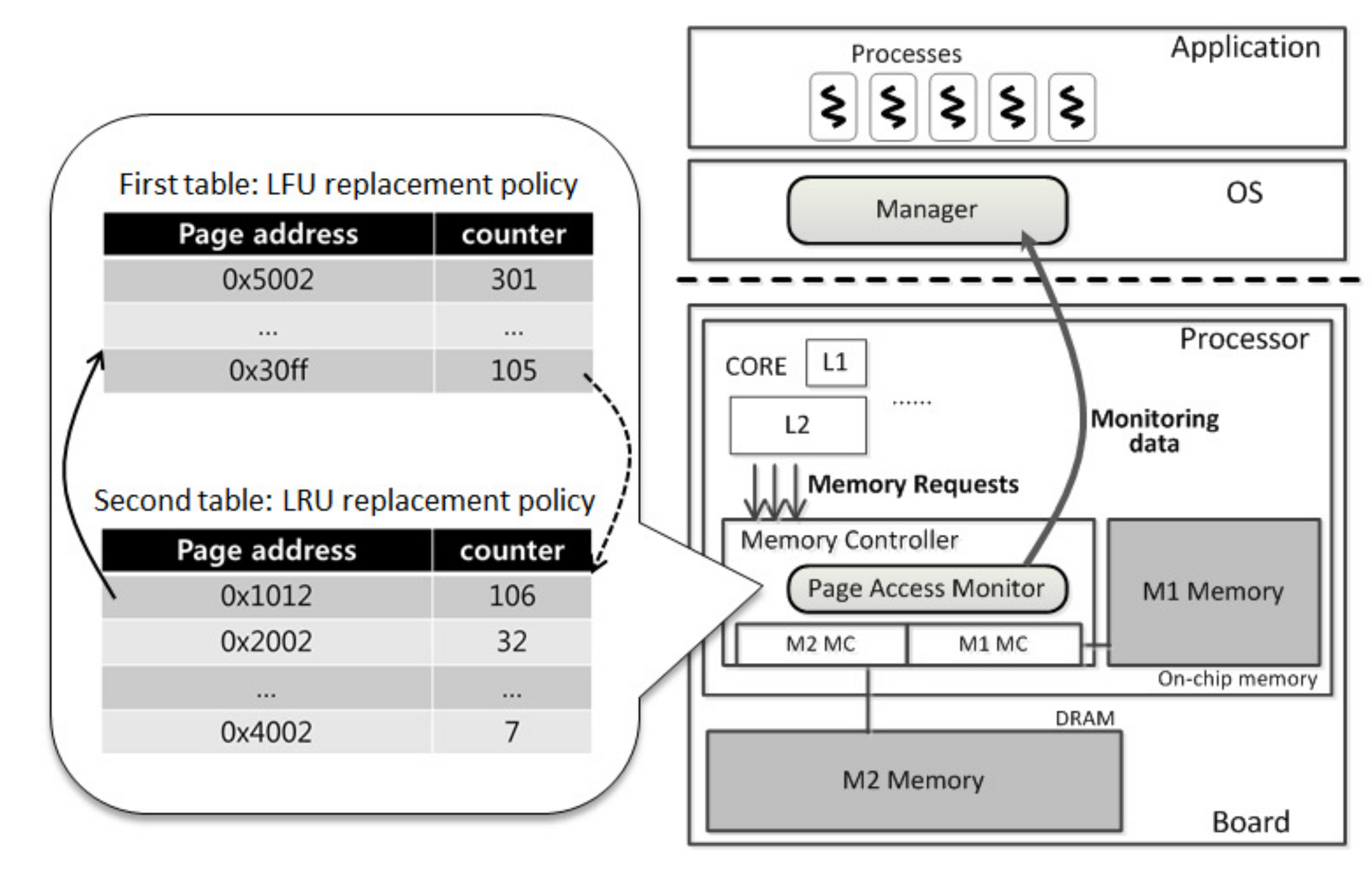
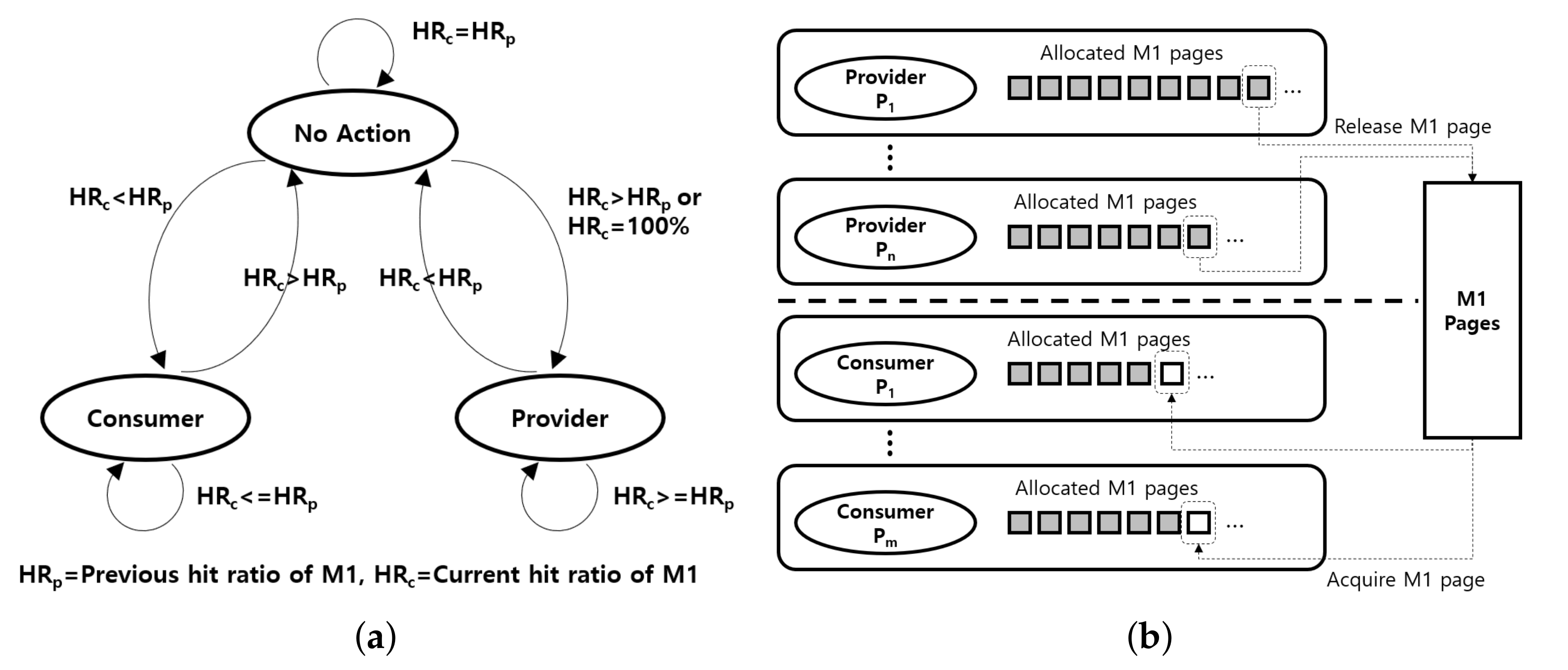
3.1. Memory Management with Monitor

To improve the performance when using the main memory with M1 memory and M2 memory, the pages that are accessed more frequently must be mapped to M1 memory. OS should attempt to allocate the most frequently used pages to M1 memory and the less frequently used pages to M2 memory. Figure 2 shows a high-level overview of the main memory management scheme through data migration between M1 and M2, which is based on periodic hardware-assisted page access monitoring. During a period, the hardware page access monitor collects information about page accesses. At the end of the period, the OS intervenes in memory management. The OS uses the collected information to determine a new mapping of pages. The key assumption of this approach is that the page access pattern during one period is similar to that in the next period. The OS moves the frequently accessed pages in M2 memory into M1 memory and the less accessed pages in M1 memory into M2 memory.
For the OS to determine the pages that must be allocated to M1 memory, the system should be able to monitor the page access pattern when the application is running. To monitor the information about the page accesses, we designed a hardware-supported monitor in a memory controller, as shown in Figure 3. The data migration between M1 and M2 is performed with the hardware-assisted page access pattern-monitoring module. Operation of the hardware-assisted page access monitor is as follows. At the hardware cache level, LLC misses cause memory requests for the missed data. These requests are handled by the hardware memory controller; thus, the memory controller can observe all the memory requests. We add a page access monitor module to the memory controller, which gathers a list of the most frequently accessed pages. This module maintains tables that include entries consisting of page addresses and counters, as shown in Figure 3. Whenever a memory request occurs, it finds the matching entry in a table with a page address and the corresponding counter value is increased by one. If there is no matching entry, a new entry is created and added to the table.
We construct two tables to monitor the page access pattern. The storage area to store tables in the memory controller must be limited because the hardware cost increases with the memory range used by a process. Consequently, the memory controller cannot log all types of accessed pages during operation. We should design a monitoring method with small tables. In the case of the first table, we designed it to contain entries of the most frequently accessed pages. It is managed with an Least Frequently Used(LFU)-like replacement policy to represent “frequency”. It always contains pages with larger count values than pages in the second table. It can contain the entries of the pages that are located in both M1 memory and M2 memory during one period. At the end of the period, all pages located in M2 memory among the pages in the first table will be moved into M1 memory. If one entry is removed from the first table by adding a new one, the count value of this page will be lost. The page access monitor cannot store the count values of removed pages without the second table, and the corresponding page also loses the chance to move to the first table when it is reaccessed in the same period. To store the history of the pages, we add the second table, which is managed by the Least Recently Used (LRU) replacement policy to represent “recency,” as shown in Figure 3.
Algorithm 1 shows how to manage the two tables for monitoring the page access pattern. When a new page is accessed, its corresponding entry is inserted with a count value of 1. If the first table has a free slot to store the entry, this entry is filled into the first table. Otherwise, a new entry of an accessed page is inserted into the Most Recently Used (MRU) position of the second table with a count value of 1. If the page is accessed and its corresponding entry is already in the first or second table, the count value of the corresponding entry is increased by 1. When the corresponding entry is in the second table, we compare the count value after increasing by 1. If the count value is greater than or equal to the minimum count value on the first table, the entry of the accessed page is moved to the first table and the entry with the minimum count value is moved to the MRU position of the second table.
Algorithm 1 Page access monitoring function.
1: T f i r s t : The first table
2: T s e c o n d : The second table
3: E p : Entry for p page, which includes page address and count value
4: C p : Count value of E p
5: M i n q : The smallest count value whose page is q on T f i r s t

6: During a period, p page is accessed
7: if E p is on T f i r s t then
8:     Increase C p by 1
9: else
10:       if T f i r s t is not full then
11:             Insert E p on T f i r s t with C p = 1
12:       else
13:           if E p is on T s e c o n d then
14:                 Increase C p by 1
15:                 Move E p to MRU position
16:           else
17:                 if T s e c o n d is full then
18:                     Remove LRU entry
19:                 end if
20:                 Put E p on MRU of T s e c o n d with C p = 1
21:           end if
22:           if C p M i n q then
23:                 Move E p on T f i r s t
24:                 Move E q on MRU of T s e c o n d
25:          end if
26:      end if
27:  end if

28:  At the end of a period, all pages on T f i r s t are moved to M1 memory. Reset all the count values of T f i r s t and T s e c o n d .
At the end of every period, the OS obtains the information of the page access pattern from the monitoring module, determines the allocations of pages for processes, and then transfers the most frequently accessed pages to M1 memory. In our scheme, the pages in the first table are the most frequently accessed pages during one period; thus, the OS will allocate all pages in the first table to M1 memory. When the OS moves the pages to M1 memory, both the pages related to M1 memory and the pages related to M2 memory in the first table should be allocated to M1 memory.

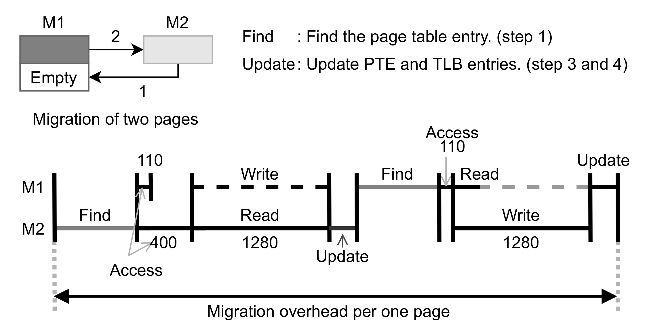
3.2. Page Migration between M1 and M2

Next, the OS intervenes in regular program execution and performs migration of the most frequently used pages of M2 into M1 memory. First, the OS obtains the list of frequently accessed pages from the memory controller. Then, the OS handles page migrations. We use a page as a migration granularity, and the migration is based on the swapping mechanism. To migrate one page, the OS performs the following processes: (i) The OS finds the page table entry related to the corresponding physical page, which can be achieved by reverse mapping (RMAP) in Linux [37,38]. (ii) The OS transfers the data to a new physical position. (iii) It replaces the physical page address in the corresponding page table entry. (iv) It updates the TLB entry that is related to the corresponding old page table entry. When the OS processes the migration of the page in M2 memory into M1 memory, the page that is the least used in M1 memory should be moved to M2 memory. Therefore, the processes described above are performed twice.

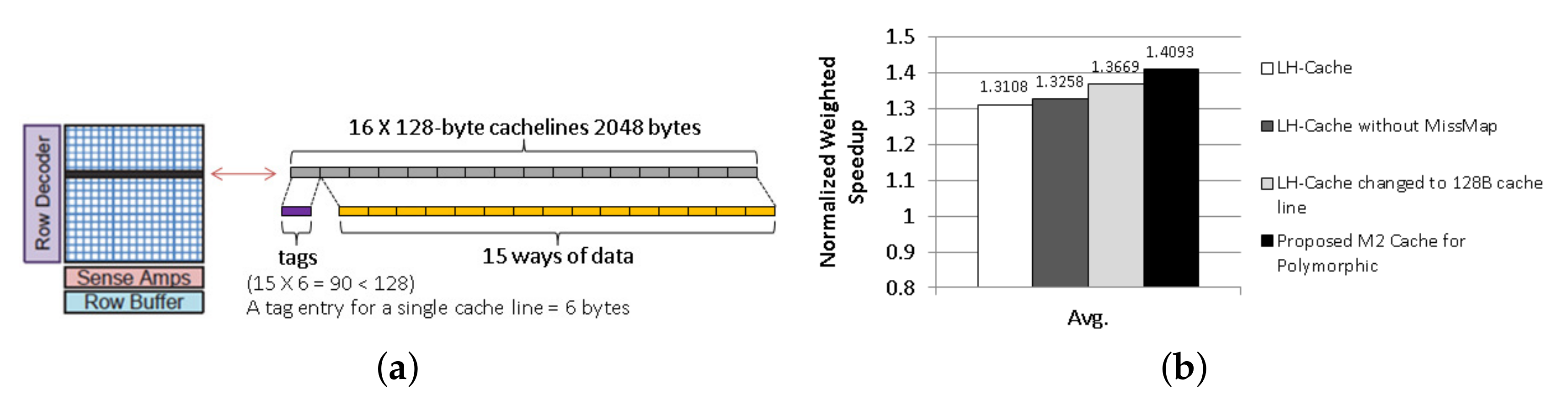
3.3. M2 Cache Management Using Part of M1

Our memory management assumes that the page access pattern during one period is similar to that in the next period. We predict that the M1 hit ratio and performance can be improved after moving the most frequently accessed pages to M1 memory. However, some memory-intensive workloads can show dynamic memory access patterns; hence, it is possible that hot pages during one period will not overlap with those during the next period. Although we designed an efficient monitoring algorithm, it uses tables of a limited size to monitor the accessed pages. As a result, misprediction can occur, which degrades the hit ratio and performance. To mitigate performance degradation due to misprediction, we design polymorphic memory in which M1 is both a part of memory and M1 cache.
If we use all of M1 as just a part of memory, the memory access performance could be degraded if misprediction and mis-migration occur in the memory management scheme owing to dynamic changes in page access patterns. One of the advantages of using a cache is that it can quickly react to dynamic changes in memory access patterns. M1 can be used as a cache for M2 because it has a much lower latency than M2. However, if we use all of M1 as an M2 cache, the cache tag overhead can be a major problem and the performance with M2 cache would be worse than that with M1 memory. If we assume that 16 MB out of 128 MB of M1 is used as an M2 cache, the performance of M1 memory is not degraded by a reduction of 16 MB because the M1 hit ratio barely changes when the size is changed from 128 MB to 112 MB for most of applications, as we identified with the benchmark experiments for cache miss rate according to M1 cache size, which is shown in Figure 4. Compared to the M2 cache with all of M1, the tag space of the 16 MB M2 cache only occupies 352 KB. In addition, this M2 cache can increase the total hit ratio of M1 by caching M2 memory accesses, especially those that are caused by misprediction. According to our memory management scheme, M1 memory can store most of the frequently accessed pages, while M2 cache stores only memory requests missed on M1 memory. Therefore, polymorphic memory can reduce both the total access counts on M2 cache and the total overhead to search for a tag in comparison with using all of M1 as an M2 cache.
Some related studies on LH-Cache [16] and Alloy Cache [17] have presented effective approaches for utilizing on-chip memory as the DRAM cache, reducing the latency when accessing the DRAM cache. However, Alloy Cache [17] is not suitable for the M2 cache in polymorphic memory because a direct-mapped cache shows lower hit ratios with a small size such as 16 MB. LH-Cache is composed of a 29-way set associative cache with a 64-byte cache line, and it uses MissMap to reduce the miss latency. According to Jiang et al. [34], the cache hit ratio increases with the cache line size; however, memory bandwidth utilization also increases. As a result, the best performance improvement is achieved with a 128-byte cache line.
Accordingly, we designed a 128-byte cache line, and the architecture of the M2 cache is similar to that of LH-Cache, as shown in Figure 5a. A one-row buffer of 2 KB is divided into 16 blocks. We designed one block for storing tags and 15 blocks for storing data because all the tags of 15 data items can be inserted into one block. We implemented a 15-way set-associative cache. Figure 5b shows the results of preliminary tests for the cache designs. LH-Cache with a 128-byte cache line shows better performance than LH-Cache. MissMap is used to reduce the miss latency by checking for the existence of data in LH-Cache before searching for tags. However, it can increase the hit latency because MissMap is always accessed for every memory access. If the hit ratio is high, the performance benefit may be lost. In addition, MissMap reduces the size of the LLC because it borrows the LLC space to store a MissMap table. Therefore, we use a 15-way set-associative cache in Figure 5a for the M2 cache of polymorphic memory. Figure 5b shows that LH-Cache without MissMap achieves better performance than LH-Cache. Our design of the M2 cache shows the best performance.

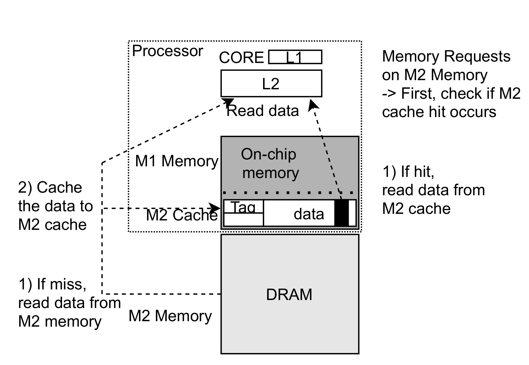
3.4. Polymorphic Memory of M1 as Both Part of Memory and M2 Cache

We designed the main memory to be exclusively arranged through the physical memory area, and the main memory is physically divided by the memory address. The physical memory address space of M1 memory is easily differentiable from that of M2 memory. By checking the physical addresses of the requested pages, memory requests can be processed on the appropriate memories. If the memory request is on M1 memory, it is directly transferred to M1 memory and the data are read from the M1 memory. At the same time, the page access monitor updates one of two tables for monitoring the page access pattern. It also updates the tables in the case of M2 memory requests.
If memory requests for accessing M2 memory occur, the operation in the memory controller should be different. The memory controller must consider the existence of an M2 cache. Therefore, if there is a memory request for accessing M2 memory, the memory controller should check whether the memory request is a hit on the M2 cache by looking up a tag array, as shown in Figure 6. If an M2 cache hit occurs, the data can be directly read from the M2 cache. If a miss occurs, the memory controller accesses M2 memory and then reads the data from M2 memory. At the same time, it caches the data into the M2 cache for the next access, as shown in Figure 6.
When we use some parts of M1 as an M2 cache, the key decision is on whether the amount of M2 cache is adequate for the cache size. If we increase the size of the M2 cache, the size of the M1 memory decreases from the fixed size of M1. Increasing misses on M1 memory caused by reducing the size of M1 memory can be absorbed into an M2 cache for which size is increased. However, increasing the hit ratio on an M2 cache results in overhead of looking up a tag array. The M2 cache needs two accesses on M1 per memory access for looking up a tag array and for reading data. Therefore, the performance will be degraded when using a large M2 cache. This is similar to using all of M1 as a cache if we use a very large M2 cache. In this case, the performance is much lower than that with all of M1 memory. In general, the performance curve becomes concave as the size of the M2 cache increases.

3.5. Multi-Process Support Management

In the case of multiple programs in a manycore environment, all the processes of the programs will attempt to obtain a greater portion of M1 memory for fast execution because M1 memory shows better performance than M2 memory. The limited size of M1 memory leads to memory contention. The OS should address the contention problem to optimize the memory access latency and bandwidth of each process by properly allocating M1 among processes. Our approach for solving the contention problem among competing processes is to partition M1 memory and to control the size of M1 memory allocated to each process.
The designed partitioning scheme for M1 memory consists of two parts: (i) categorizing processes with several levels by monitoring memory usage information and (ii) determining the allocated size of M1 memory for each process. We modified the memory controller such that it monitors the counts of memory accesses of M1 memory and M2 memory per core. With these memory access counts, the OS calculates the M1 hit ratio during a period. We categorize a process into three states with the hit ratio of M1 and compare the current M1 hit ratio with the previous one: a provider, a consumer, and a no-action state. A provider is a process that can give some portion of M1 memory to other processes, and a consumer requires more M1 memory for data processing.
The categorizing algorithm and state diagram of each process are shown in Figure 7a, and the M1 memory balancing procedure between processes through M1 partitioning and allocation is shown in Figure Diagramb. If the current hit ratio of a process is higher than the previous one or if it is 100%, we classify this process as a provider. This means that, during the current period, more requests are hits on M1 memory than in the previous period, or the memory coverage of the process becomes so small that the most frequently accessed pages are concentrated in M1 memory. In this case, we predict that this process has sufficient M1 memory. Therefore, we define this process as a provider, and it releases the portion of M1 memory allocated to it. By contrast, if the current hit ratio is lower than the hit ratio of the previous period, we set it as a consumer state. This means that the amount of M1 memory required for this process is not sufficient for it to run efficiently. The consumer allocates the portion of M1 memory provided by the provider as its own. Although a consumer obtains some portion of M1 memory from providers, it is possible not to increase its hit ratio of M1 memory by changing the memory access patterns. If the hit ratio does not increase, we classify it as a consumer again in order to obtain more M1 memory. Similarly, in the case of a provider, we classify it as a provider again if its M1 hit ratio is increased after providing some portion of M1 memory to the consumers.
Meanwhile, when the M1 hit ratio of the consumer increases after it obtains a small part of M1 memory, we do not directly change it to a provider. The M1 hit ratio is normally increased by increasing M1 memory. If we assign this process as a provider directly, it will lose some portion of M1 memory and its M1 hit ratio will decrease during the next period. This can cause the ping-pong problem because this process will be a consumer again. Therefore, we add the no-action state to the state diagram, as shown in Figure 7.
After determining the states of the processes, we recalculate the amount of M1 memory that belongs to each process and reallocate them between providers and consumers. The providers send their M1 memory pages to the consumers. The total size of the change in M1 memory is equal to the maximum number of page migrations; we set the total number of migrations as 100 pages. For example, if there are two providers and one consumer, each provider gives 50 pages of M1 memory to the consumer, and the consumer receives 100 pages of M1 memory from the two providers.

4. Evaluation

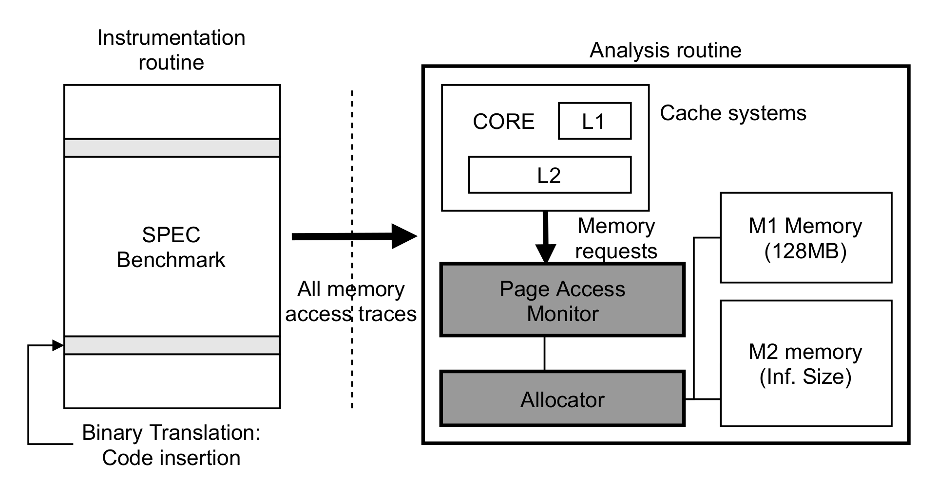
4.1. Simulation Environment

To evaluate the proposed memory management techniques for polymorphic memory, we developed a simulator based on Pin [39], which is well-known tool for the dynamic instrumentation of applications. The Pintool can used for profiling and performance evaluation for architecture-specific details, so it is suitable for testing the dynamic cache and memory system with 3D stacked DRAM. Pin is publicly available for Linux platforms. To evaluate the performance of our management schemes, we first define the architecture with Pintool, in which we assume that a processor has four cores with L1 and L2 caches, M1 on-chip memory, and memory controllers for M1 and M2, as shown in Figure 8. The M2 memory is an on-board DRAM memory similar to DDR3. Each core has its private 32 KB L1 cache and 512 KB L2 cache. We assume that the L2 cache is private to evaluate the performance using only memory management. M1 has a size of 128 MB, and we assume that M2 has an infinite size. The detailed experimental configurations are listed in Table 1.
We used the SPEC CPU2006 benchmark [40] for the evaluation workloads. All the benchmarks were compiled with gcc 4.4.5. All the simulations were run with real data sets. With the SPEC CPU2006 benchmark, we used Pin to create a simulator and to extract all memory traces when running the SPEC CPU2006 workloads. Pin is organized with two routines, namely an instrumentation routine and an analysis routine, as shown in Figure 8. When running an application, Pin extracts all instructions and transfers all load instructions to the analysis routine. We performed the analysis routine by adding our memory architecture including the designed cache systems. The designed page access monitor and memory allocator for migration are added to this architecture.
Before performing the evaluation, we tried to classify the benchmark programs into several groups. To this end, we extracted both counts of memory requests and how many pages were used during 5 billion cycles, and we examined the access frequency, which was calculated as the average of access counts, and the page coverage, which is the number of pages used. Table 2 summarizes the results. We classified workloads into three categories based on the access frequency and page coverage. First, we divided the workloads by access frequency; then, we divided the workloads that showed high frequency into two groups by page coverage. These two groups are group 1, which shows high frequency and large coverage, and group 2, which shows high frequency and small coverage. Finally, group 3 includes workloads with low frequency.

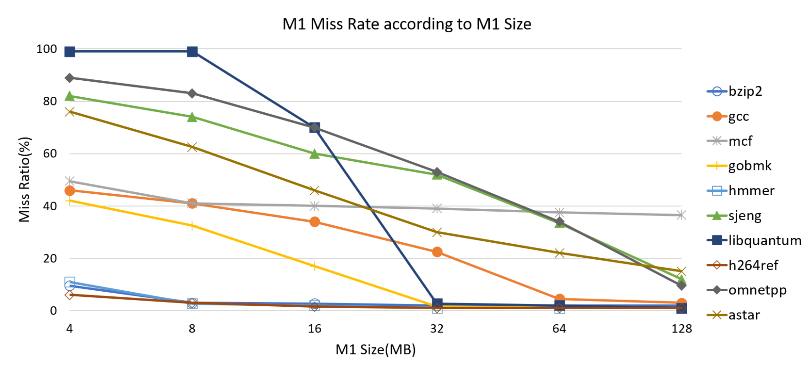
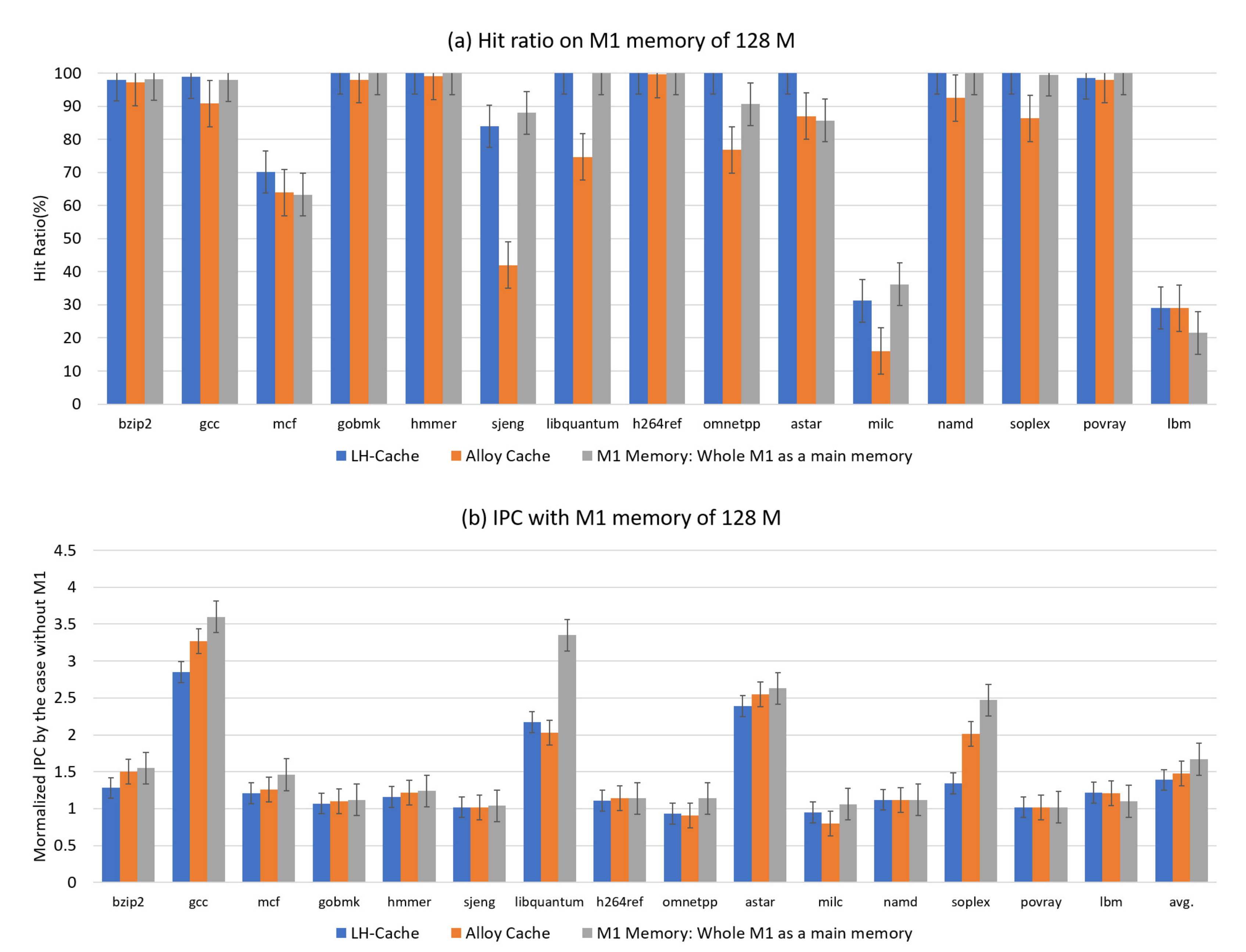
4.2. Evaluation of Memory Management with M1 as Part of Memory

In this section, we present the performance results of our techniques for the main memory. As workloads for evaluation, we selected the SPEC CPU2006 benchmark [40].

4.2.1. Analysis of Migration Overhead

First, we analyzed the migration overhead of our memory management scheme. In every period, migration is operated by swapping pages between M1 memory and M2 memory. Migration includes many memory accesses to change the page tables and TLB updates; hence, it increases the total operation time. To analyze the overhead of a page migration, we first checked how many memory accesses are needed to find the page table entry by the OS. According to [37], RMAP does not provide a direct method of linking the physical page and the page table entry but requires many memory accesses. A page descriptor corresponding to the physical page points to the anon_vma data structure, which is the starting point of the RMAP. Further, anon_vma points to a memory region descriptor, i.e., the vm_area_struct data structure, and the field vm_mm in vm_area_struct points to another memory region descriptor, i.e., the mm_struct data structure. The mm_struct data structure includes a field pgd that contains the address of the Page Global Directory. To find the address of the Page Global Directory, four memory accesses are needed. For 64-bit architectures, four levels of paging are used in Linux. Therefore, four memory accesses are additionally needed to find the page table entry. Finally, the OS should perform eight memory accesses for the first step.
During the second procedure, data copy overhead will occur. The data copy overhead can be calculated using the memory access time and time to transfer data. Because M2 memory has a large latency and low bandwidth, the data copy overhead is bounded to the M2 access latency and data transfer time. With a 4 GHz CPU and 12.8 GB/s of bandwidth of M2 memory (see Table 1), it takes 1280 cycles to transfer one page and its access latency is 400 cycles. Finally, replacing the corresponding page table entry with a new physical page address and updating the TLB entry are the remaining tasks. Replacing the value of the page table entry requires one memory operation, and the overhead of updating TLB is approximately 127 cycles [21,41].
Figure 9 shows the total overhead of one-page migration. We assumed that a frequently accessed page in M2 memory is first moved into an empty slot in M1 memory and that a rarely accessed page in M1 memory is then moved into the place at which the frequently accessed page was located. This means that we should calculate twice the time needed to transfer data and the memory access times of M1 memory and M2 memory. In addition, we should calculate twice the overheads for steps 1, 3, and 4, as shown in Figure 9. We assumed that all the memories for storing pages are in M1 memory; hence, the overhead of memory access was calculated as 110 cycles. The total overhead per page in a cycle can be calculated by
C T o t a l = C F i n d 2 + C U p d a t e 2 + ( 400 + 1280 ) + ( 110 + 1280 )
where C F i n d = 110 8 and C U p d a t e = 110 + 127 . Finally, we calculate the migration overhead for one-page migration as 5304 cycles. At the end of every period, the total number of pages that should be moved by the OS is determined by the number of pages of M2 memory in the first table. The migration overhead is calculated by multiplying C T o t a l by the total number of moved pages.
According to these analyses, we measured the migration overhead as a percentage of the total operation time, and the results are summarized in Table 3. In the table, except for the milc and lbm benchmark workloads, most of the workloads have a small migration overhead that accounts for less than 1% of the operation time. Milc and lbm show dynamically changed access patterns; hence, misprediction occurs repeatedly. As a result, the OS moves many pages at the end of the period, and this increases the migration overhead. Thus, in summary, from the experimental results, we determined that the total migration overhead accounts for less than 1% of the operation cycles of most of the workloads.

4.2.2. Performance with a Single Workload

For the memory management of M1 as a part of the memory, we first show the performance with a single workload. We compared the Instructions Per Cycle (IPC) when using all of M1 as a part of the memory with the IPC when using all of M1 as a DRAM cache with LH-Cache and Alloy Cache. For these experiments, we conducted a full simulation with our simulator. Figure 10 shows the results of hit ratios on M1 and performance. In this evaluation, M1 memory means that all of M1 is used as the main memory and is managed by our migration policy. We measured the cache hit ratio and IPC of each benchmark running for the three M1 configurations, and the results are plotted in Figure 10. Figure 10a shows the hit ratio of three configurations, namely LD-Cache, Alloy Cache, and M1 as a part of the memory. As shown in the figure, LH-Cache has the highest cache hit ratio. In the case of LH-Cache, the requested data will be immediately loaded into the cache when the memory request is missed. As a result, it can quickly react to dynamically changing memory access patterns. By contrast, in the case of M1 as a part of the memory, the most frequently accessed pages are predicted by monitoring page access patterns during a period, and we then migrate those pages. In the next period, the page access patterns can be changed so that the M1 hit ratio can be reduced, i.e., it is lower than that of LH-Cache. Alloy Cache shows a low hit ratio compared to LH-Cache and M1 memory because it uses the direct-mapped cache.
Figure 10b shows the normalized IPC of each benchmark, which also gives the error range of each experimental result. As shown in the figure, our M1 management scheme shows the highest IPC among the three configurations for most of the benchmarks. Although LH-Cache can reduce access latency by making a row buffer hit and, with MissMap, it still needs two accesses on M1, however, M1 memory guarantees direct access to data because the memory data can be read by the memory address. Therefore, M1 memory needs fewer cycles than LH-Cache when accessing data on M1, resulting in better performance. Our policy can improve the performance by an average of 13.7% with 0.8 standard deviation for the normalized IPC value. The reason for the large standard deviation is due to the large difference in performance improvement for each benchmark. For instance, the performance improvement of libquantum is 54.2% compared to that of LH-Cache, while namd has little improvement.
Among the workloads shown in Figure 10, gobmk, hmmer, sjeng, h264ref, namd, and povray are classified as group 3. These workloads show small improvements in performance. If we use 128 MB of M1 memory, most workloads of group 3 show nearly 100% hit ratios on M1 memory because they have a small memory footprint. In addition, they show low frequency during a period. If we compare the performance improvement with the results of group 2, we can see that the performance is significantly affected by frequency. Except for the case of Alloy Cache, Bzip2, gcc, and libquantum also show nearly 100% hit ratios. However, these performances are improved significantly. In the case of Alloy Cache, the hit ratio is reduced because the high frequency causes large misses. With the same hit ratios on LH-Cache and M1 memory, a higher frequency implies larger hit counts on M1. The overhead when a memory request is a hit on LH-Cache is larger than that when a memory request is a hit on M1 memory. Therefore, the accumulated overhead of LH-Cache becomes much larger than that of M1 memory as the number of hit counts on M1 increases. Consequently, the performance of M1 memory will be better than that of LH-Cache and Alloy Cache.
Workloads in group 1, such as mcf, omnetpp, astar, milc, and soplex, can also improve the performance. However, the improvements for workloads in group 1 were lower than those for the workloads in group 2. Because of the large coverage, the workloads in group 1 show lower M1 hit ratios than the others. In addition, the hit ratios on LH-Cache are larger than those on M1 memory, as shown in Figure 10a. Although the overhead of hits on LH-Cache is larger than that of accessing M1 memory directly, it is smaller than the overhead of accessing M2 memory. For the workloads of group 1, the improvement in the performance of M1 memory is reduced because the hit ratios on M1 memory are much lower than those on LH-Cache. Milc shows the largest difference between hit ratios on M2 cache and M1 memory. As a result, the performance improvement is the least among the workloads of group 1. Further, lbm, which is in group 2, shows the largest difference through all the workloads, and the performance of M1 memory is lower than that of DRAM caches such as LH-Cache and Alloy Cache.

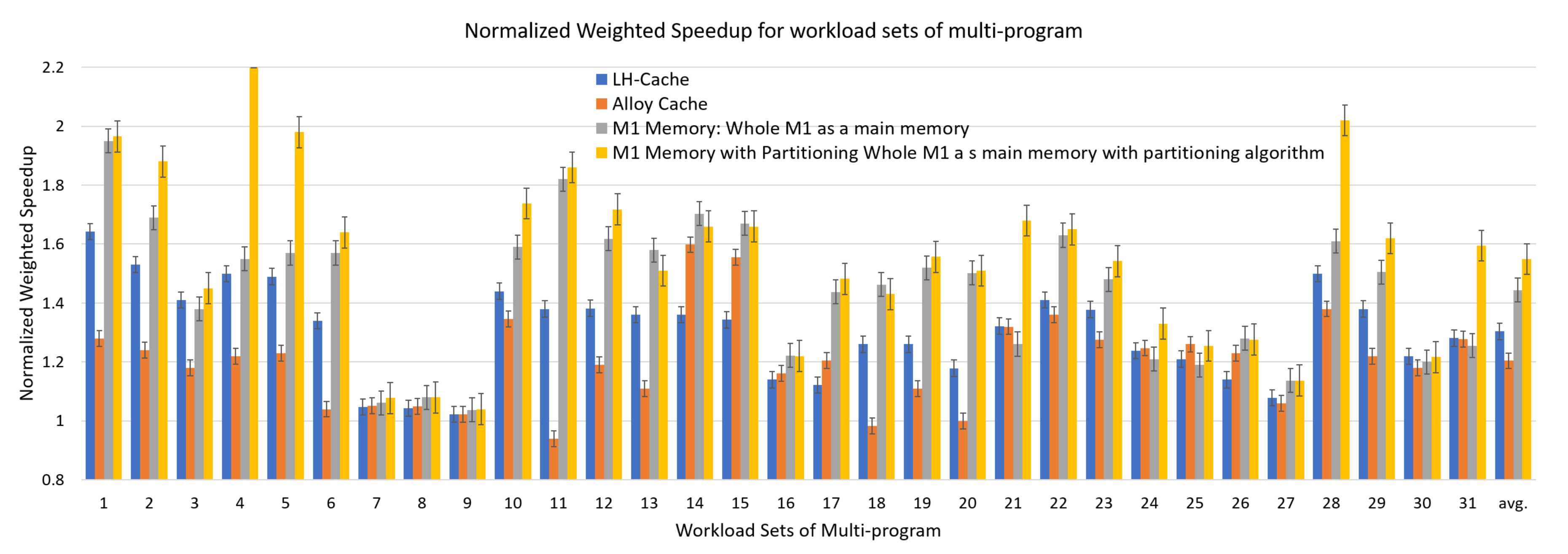
4.2.3. Performance with Multiple Workloads

To evaluate the performance of memory management in a multi-process environment, we used many sets with multi-programmed workloads. Table 4 summarizes 31 sets of workloads. To make various sets of multi-programmed workloads, we combined workloads from all the groups. Sets 1, 2, and 3 mix the workloads from group 1, and sets 4, 5, and 6 mix the workloads from group 2. Sets 10 to 13 were selected from both group 1 and group 2. In this manner, we created 31 sets of multi-programmed workloads with various combinations.
We measured the performance of the management policy of M1 memory using the weighted speedup [42] equation, as follows.
W e i g h t e d S p e e d u p = i I P C s h a r e d , i I P C a l o n e , i .
All the experiments were conducted for 5 billion cycles, including 1 billion cycles for warming up. Figure 11 shows the normalized weighted speedup for all the workloads from sets 1 to 31, and the overall average speedup is plotted at the right end of the figure. We normalized the performance results by the results of the case with no M1 memory. The x-axis represents the number of sets, including the average values, and the y-axis represents the normalized weighted speedup. In this evaluation, M1 memory means that only M1 memory management is applied which only has monitoring and migrating pages between M1 and M2, while M1 memory with partitioning represents the results of memory management that has M1 partitioning and the dynamic allocation algorithm.
The results show that the performance of M1 memory is better than that of DRAM cache, including LH-Cache and Alloy Cache for most of the workload sets. However, some workload sets, such as 3, 30, and 31, show lower performance than that of LH-Cache. Workloads that have a relatively low frequency among the four workloads will lose M1 memory by contention. In workload sets 3, 30, and 31, milc and lbm are workloads with relatively low frequencies. In addition, they show dynamically changed access patterns. Therefore, with small M1 memory and dynamically changed access patterns, the M1 hit ratio and performance are degraded. From the results, we conclude that the proposed partitioning and dynamic allocation algorithm can guarantee that a proper amount of M1 memory is allocated to each workload. Compared to LH-Cache, the performance of M1 memory with partitioning can be increased by 35.1% at most. On average, the performance improvement was 17.6% with 0.3 standard deviation for the normalized data. Even if the workloads have low frequency, they can obtain some M1 memory to store their hot pages. As a result, workload sets 3, 30, and 31 can improve their performance with a partitioning algorithm. However, this can limit workloads that show high frequency to take M1 memory from workloads with low frequency. Therefore, the total performance may be degraded, as in the case of sets 13 and 14. However, most of the workload sets show better performance with the partitioning algorithm.

4.3. Evaluation for Polymorphic Memory System

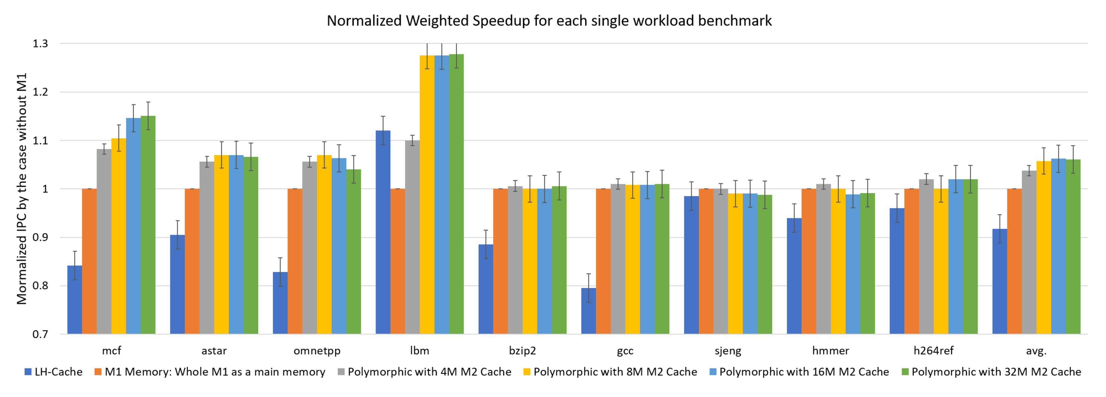
4.3.1. Performance with a Single Workload

Next, we evaluated the results of the polymorphic memory system, in which M1 is used both as M2 cache and a part of the memory region. First, we evaluated the improvement of the polymorphic memory with a single workload with the variation of M2 cache size from 4 MB to 32 MB. Figure 12 shows the performance results with a single workload. The results are normalized by the case with M1 memory and compared with various M2 cache sizes. We sorted the workloads on the x-axis according to their groups.
The last three workloads, sjeng, hmmer, and h264ref, are in group 3, in which access frequency is low. As shown in Table 2, the performance is degraded when the polymorphic memory is employed. First, hmmer and h264ref have a small memory footprint; hence, they show nearly 100% of the hit ratio on M1, as shown in Figure 10a. However, the small memory footprint is not the main cause of performance degradation when using the polymorphic memory. The M2 cache reduces the amount of M1 memory in the polymorphic memory because the total size of M1 is 128 MB. Some accessed pages that were located in M1 memory when all of M1 is used as the main memory will be located in the M2 cache in the polymorphic memory, and they produce a larger overhead at every hit compared to the hit latency on M1 memory. In the case of sjeng, its memory footprint is larger than the memory size of M1. At low frequencies, the performance gain when using an additional portion of the M2 cache cannot be higher than the overhead of the two accesses. Therefore, we cannot achieve performance improvement by using the polymorphic memory through the workloads in group 3.
Meanwhile, the workloads in groups 1 and 2 show performance improvements when using the polymorphic memory, as shown in Figure 12. These workloads have a high frequency of memory accesses; hence, the polymorphic memory is useful in improving performance. If we compare the results of omnetpp and gcc, omnetpp achieves a higher performance gain than gcc. Although the two workloads show similar frequencies, omnetpp shows a larger coverage than gcc, meaning that the number of misses on M1 memory of omnetpp can be larger than that of gcc. These missed accesses are absorbed into the M2 cache. Therefore, omnetpp can achieve a larger performance improvement by the existing M2 cache than gcc. We achieved a higher performance improvement with the workloads in group 1 than in group 2.
Finally, mcf and lbm also show high performance improvements with the polymorphic memory. The two workloads show a very dynamically changed access pattern, causing misprediction. However, by using the polymorphic memory, we can improve the performance significantly. Among the workloads in group 1, mcf shows greater improvement because it will cause much larger misses on M1 memory than others. For the same reason, lbm can also achieve a large performance gain when using the polymorphic memory. As shown in Figure 12, lbm shows the best performance improvement when using the polymorphic memory.

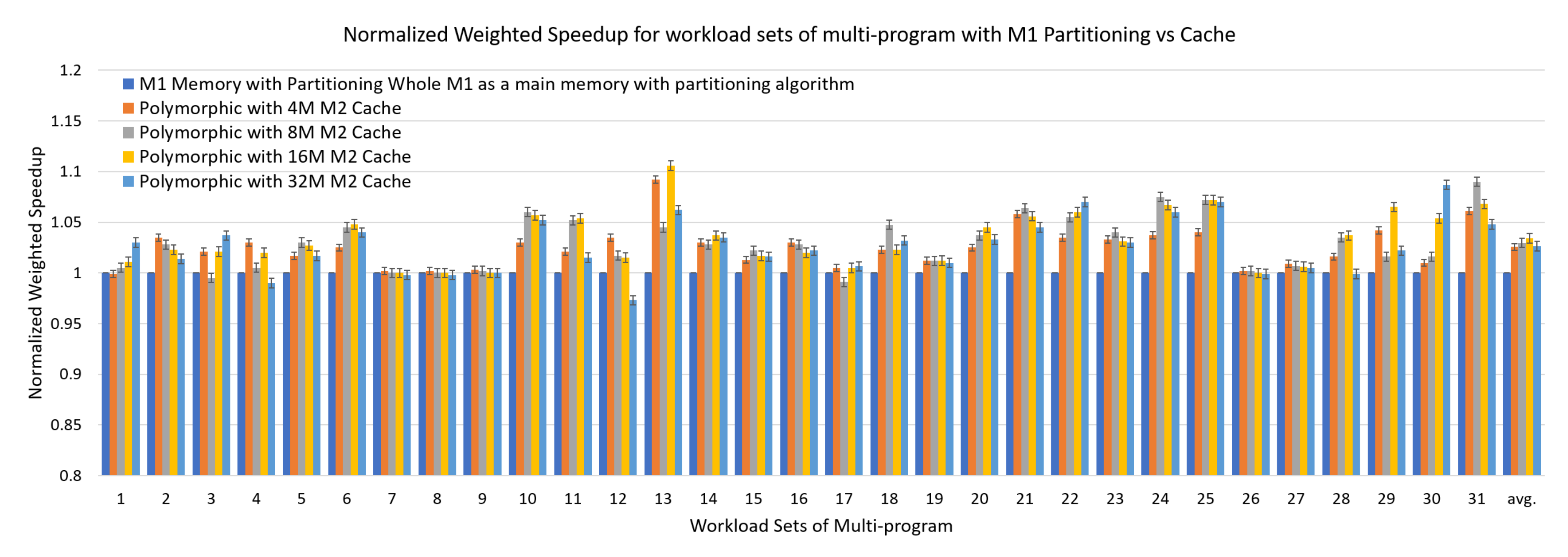
4.3.2. Performance with Multiple Workloads

Next, we evaluated the results of the polymorphic memory system with multiple workloads. Figure 13 shows the performance results in the case of multiple workloads. We normalized the performance results by the results of M1 memory with partitioning and compared the results of the polymorphic memory with various cache sizes. On average, the performance curve becomes concave as the size of the M2 cache increases. When the size of the M2 cache is 16 MB, the average performance is the best and the performance improvement is 3.35% compared to that of M1 memory with partitioning. In addition, compared to M1 memory with partitioning, the performance of the polymorphic memory can be improved by 10.6% at most. On average, the performance improvement is 3.35% when we use a 16 MB M2 cache. Compared to LH-Cache, the maximum improvement of the polymorphic memory is 41% and the average improvement is 21.7% with 0.026 standard deviation for the normalized results.
Workload sets 7, 8, and 9 consist of only workloads in group 3; hence, they have low frequency. Similar to the results of a single case, the results of multiple workloads also show that the polymorphic memory cannot improve performance. Workload sets 26 and 27 include three workloads in group 3 among the four workloads, and their performance barely improved. However, most workload sets show a performance improvement.
While a single workload in group 1 can achieve a large performance improvement using the polymorphic memory, multiple workloads that consist of only workloads in group 1 cannot achieve a large performance improvement, as shown in Figure 13. By contrast, the workload sets with groups 1 and 3 or with groups 2 and 3, such as sets 13, 21, 22, and 31, show a large performance improvement. However, workload sets 4, 5, and 6 show good performance improvement, and these sets were mixed with workloads in group 2. Sets 1, 3, and 30 show that the performance improves as the M2 cache size increases. This is because the M2 cache with a small size causes cache thrashing. Workload sets 1, 3, and 30 have very high frequency and large coverage. Therefore, a small cache will cause large misses and the performance will be degraded.

4.4. Summary and Dicussion

This section summarizes and discusses the experimental results and performance improvements for the proposed schemes applied in the experiments. Table 5 summarizes the results of experiments on workload sets for various schemes designed in this paper on the usage of M1 memory. First, the experimental results for the case where M1 is used as only part of memory are summarized as follows. When M1 is used as a part of memory, a dynamic migration method between M1 and M2 can be applied for a single workload, and in this case, performance is improved by 13.7% compared to the existing cache only scheme. For multiple workload sets, performance is improved up to 17.6% by applying M1 partitioning and dynamic page allocation between processes.
Next, the experimental results for the case of using M1 as a polymorphic memory that is a mixture of M2 cache and part of memory are summarized as follows. When M1 is used as a polymorphic memory which uses a portion of M1 as cache and a portion of M1 as part of memory, the hybrid approach results in an average performance improvement of 15.7% over the previous caching-only scheme for the single workload set. Moreover, in the case of multiple workload sets, applying M1 partition and dynamic allocation between multiple processes in addition to the hybrid approach results in an average improvement of 21.7% in performance. In summary, for a multi-core memory contention system in which multiple-processes are operated competitively, 3D-stacked DRAM can be used as a polymorphic memory with a hybrid of cache and part of memory, and dynamic M1 partitioning between processes, which improves overall system performance.

5. Conclusions

Recently, manycore computing systems are widely applied to running data-intensive applications. The key challenge for these computing systems is how to utilize large amounts of memory with high bandwidth because most applications require large amounts of main memory. In these systems, 3D stacked on-chip DRAM is increasingly used to overcome the data processing performance between the processor and memory. Many existing studies have been applied to 3D stacked DRAM, being used as a cache of general memory or as a NUMA architecture along with general memory. However, not many existing studies have used the on-chip DRAM as a hybrid memory with a cache and flat address region, furthermore, little studies have investigated dynamic memory allocation of stacked DRAM for manycore systems.
In this paper, we proposed a polymorphic memory system of 3D stacked DRAM which employ dynamic memory allocation of 3D stacked DRAM in both as cache and the flat address region. To deal with a main memory consisting of M1 memory and M2 memory, we added a page access monitoring module to the memory controller. At the end of every period, the OS obtains the information of page access patterns from the monitoring module, partitions the M1 memory for each process according to the change in the hit ratio, and then migrates the most frequently accessed pages of each process into M1 memory. We applied the design of an M2 cache and determined its appropriate size in the polymorphic memory system. In addition, to solve the contention problem between processes in multi-process system, the states of the process are categorized and the M1 memory is dynamically allocated according to the state of each process. The management scheme can improve the performance by an average of 17.6% over LH-Cache. In addition, our experimental results showed that the polymorphic memory can improve the performance by an average of 21.7%.
The proposed system shows the efficiency of dynamic allocation and hybrid use 3D stacked DRAM in a multi-process system. However, the cache replacement method and the cache mapping scheme applied in this system could be limited by tag size, and it could have limitations in lazy adaptation of data migration by OS for each period. In the future, we plan to conduct additional research to address those limitations.

Author Contributions

Conceptualization, H.S., S.-H.L., and K.-W.P.; methodology, H.S.; software, H.S.; validation, H.S., S.-H.L., and K.-W.P.; formal analysis, H.S., S.-H.L., and K.-W.P.; investigation, H.S., S.-H.L., and K.-W.P.; resources, H.S., S.-H.L., and K.-W.P.; data curation, H.S., S.-H.L., and K.-W.P.; writing—original draft preparation, H.S.; writing—review and editing, S.-H.L. and K.-W.P.; visualization, H.S., S.-H.L., and K.-W.P.; supervision, S.-H.L. and K.-W.P.; project administration, H.S., S.-H.L., and K.-W.P. All authors have read and agreed to the published version of the manuscript.

Funding

This work was supported by the National Research Foundation of Korea (NRF) grant funded by the Korea Government (MSIT) (NRF-2019R1F1A1057503). This work was supported by Hankuk University of Foreign Studies Research Fund. This work was supported by the National Research Foundation of Korea (NRF) grant funded by the Korea Government (MSIT) (NRF-2020R1A2C4002737).

Conflicts of Interest

The authors declare no conflict of interest.

Abbreviations

The following abbreviations are used in this manuscript:
ITRSInternational Technology Roadmap for Semiconductors
CHOPCaching HOt Pages
TADTag and Data
PAMParallel Access Model
RMAPreverse mapping
LLCLast-Level Cache
IPCinstruction per cycle
TLBTranslation Lookaside Buffer
DRAMDynamic Random Access Memory
SRAMStatic Random Access Memory
DDRDouble Data Rate
OSOperating System
LRULeast Recently Used
LFULeast Frequently Used
MRUMost Recently Used
IPCInstructions Per Cycle
GBGiga Byte
SEPCStandard Performance Evaluation Corporation
CPUCentral Processing Unit
bzipBasic Leucine Zipper
gccGNU Compiler Collection, C Language optimizing compiler
mcfCombinatorial optimization/Single-depot vehicle scheduling
sjengsjeng chess programming
omnetppDiscrete Event Simulation
astarpath-finding algorithms program
milcMIMD Lattice Computation (MILC) collaboration
lbmLattice Boltzmann Method to simulate incompressible fluids in 3D
soplexa linear program using the Simplex algorithm
hmmerstatistical models of multiple sequence alignments
h264refa reference implementation of H.264/AVC (Advanced Video Coding)
libquantuma library for the simulation of a quantum computer
NUMANNon-Uniform Memory Access

References

  1. Park, K.H.; Park, Y.; Hwang, W.; Park, K.-W. Mn-mate: Resource management of manycores with dram and nonvolatile memories. In Proceedings of the 12th IEEE International Conference on High Performance Computing and Communications (HPCC), Melbourne, Australia, 1–3 September 2010; pp. 24–34. [Google Scholar]
  2. Borkar, S. Thousand core chips: A technology perspective. In Proceedings of the 44th Annual Design Automation Conference, San Diego, CA, USA, 4–8 June 2007; pp. 746–749. [Google Scholar]
  3. Liu, R.; Klues, K.; Bird, S.; Hofmeyr, S.; Asanović, K.; Kubiatowicz, J. Tessellation: Space-time partitioning in a manycore client os. In Proceedings of the First USENIX Conference on Hot Topics in Parallelism, Berkeley, CA, USA, 30–31 March 2009; p. 10. [Google Scholar]
  4. Boyd-Wickizer, S.; Chen, H.; Chen, R.; Mao, Y.; Kaashoek, F.; Morris, R.; Pesterev, A.; Stein, L.; Wu, M.; Dai, Y.; et al. Corey: An operating system for many cores. In Proceedings of the 8th USENIX Conference on Operating Systems Design and Implementation, Carlsbad, CA, USA, 8–10 October 2008; pp. 43–57. [Google Scholar]
  5. Kozyrakis, C.; Kansal, A.; Sankar, S.; Vaid, K. Server engineering insights for large-scale online services. IEEE Micro 2010, 30, 8–19. [Google Scholar] [CrossRef]
  6. Ousterhout, J.; Agrawal, P.; Erickson, D.; Kozyrakis, C.; Leverich, J.; Mazières, D.; Mitra, S.; Narayanan, A.; Parulkar, G.; Rosenblum, M.; et al. The case for ramclouds: Scalable high-performance storage entirely in dram. SIGOPS Oper. Syst. Rev. 2010, 43, 92–105. [Google Scholar] [CrossRef]
  7. Chang, F.; Dean, J.; Ghemawat, S.; Hsieh, W.C.; Wallach, D.A.; Burrows, M.; Chandra, T.; Fikes, A.; Gruber, R.E. Bigtable: A distributed storage system for structured data. ACM Trans. Comput. Syst. 2008, 26, 1–26. [Google Scholar] [CrossRef]
  8. Choi, J.H.; Park, K.-W.; Park, S.K.; Park, K.H. Multimedia matching as a service: Technical challenges and blueprints. In Proceedings of the 26th International Technical Conference on Circuits/Systems, Computers and Communications, Gyeongju, Korea, 19–22 June 2011. [Google Scholar]
  9. Memcached: A Distributed Memory Object Caching System. Available online: http://memcached.org/ (accessed on 1 June 2019).
  10. Wulf, W.A.; Mckee, S.A. Hitting the memory wall: Implications of the obvious. Comput. Archit. News 1995, 23, 20–24. [Google Scholar] [CrossRef]
  11. Black, B.; Annavaram, M.; Brekelbaum, N.; DeVale, J.; Jiang, L.; Loh, G.H.; McCaule, D.; Morrow, P.; Nelson, D.W.; Pantuso, D.; et al. Die stacking (3d) microarchitecture. In Proceedings of the 39th Annual IEEE/ACM International Symposium on Microarchitecture, Orlando, FL, USA, 9–13 December 2006; pp. 469–479. [Google Scholar]
  12. Kgil, T.; Saidi, A.; Binkert, N.; Dreslinski, R.; Mudge, T.; Reinhardt, S.; Flautner, K. Picoserver: Using 3d stacking technology to enable a compact energy efficient chip multiprocessor. In Proceedings of the 12th ACM international conference on Architectural support for programming languages and operating systems (ASPLOS XII), New York, NY, USA, 21–25 October 2006; pp. 117–128. [Google Scholar]
  13. Loh, G.H. 3D-stacked memory architectures for multi-core processors. In Proceedings of the 35th International Symposium on Computer Architecture, Beijing, China, 21–25 June 2008; pp. 453–464. [Google Scholar]
  14. Liu, C.; Ganusov, I.; Burtscher, M.; Tiwari, S. Bridging the processor-memory performance gap with 3d ic technology. IEEE Des. Test Comput. 2005, 22, 556–564. [Google Scholar] [CrossRef]
  15. Loi, G.L.; Agrawal, B.; Srivastava, N.; Lin, S.-C.; Sherwood, T.; Banerjee, K. A thermally-aware performance analysis of vertically integrated (3-d) processor-memory hierarchy. In Proceedings of the 43rd Annual Design Automation Conference, San Francisco, CA, USA, 24–28 July 2006; pp. 991–996. [Google Scholar]
  16. Loh, G.H.; Hill, M.D. Efficiently enabling conventional block sizes for very large die-stacked dram caches. In Proceedings of the 44th Annual IEEE/ACM International Symposium on Microarchitecture, Porto Alegre, Brazil, 4–7 December 2011; ACM: New York, NY, USA, 2011; pp. 454–464. [Google Scholar]
  17. Qureshi, M.K.; Loh, G.H. Fundamental latency trade-off in architecting dram caches: Outperforming impractical sram-tags with a simple and practical design. In Proceedings of the 45th Annual IEEE/ACM International Symposium on Microarchitecture, Vancouver, BC, Canada, 1–5 December 2012; pp. 235–246. [Google Scholar]
  18. Huang, C.; Nagarajan, V. ATCache: Reducing DRAM cache latency via a small sram tag cache. In Proceedings of the 23rd International Conference on Parallel Architectures and Compilation, Edmonton, AB, Canada, 24–27 August 2014; pp. 51–60. [Google Scholar]
  19. Vasilakis, E.; Papaefstathiou, V.; Trancoso, P.; Sourdis, I. Decoupled fused cache: Fusing a decoupled LLC with a DRAM cache. ACM Trans. Archit. Code Optim. 2019, 15, 1–23. [Google Scholar] [CrossRef] [Green Version]
  20. Yu, X.; Hughes, C.J.; Satish, N.; Mutlu, O.; Devadas, S. Banshee: Bandwidth-efficient DRAM caching via software/hardware cooperation. In Proceedings of the 2017 50th Annual IEEE/ACM International Symposium on Microarchitecture (MICRO), Boston, MA, USA, 14–17 October 2017; pp. 1–14. [Google Scholar]
  21. Dong, X.; Xie, Y.; Muralimanohar, N.; Jouppi, N.P. Simple but effective heterogeneous main memory with on-chip memory controller support. In Proceedings of the 2010 ACM/IEEE International Conference for High Performance Computing, Networking, Storage and Analysis, New Orleans, LA, USA, 13–19 November 2010; pp. 1–11. [Google Scholar]
  22. Chou, C.C.; Jaleel, A.; Qureshi, M.K. CAMEO: A twolevel memory organization with capacity of main memory and flexibility of hardware-managed cache. In Proceedings of the 47th Annual IEEE/ACM International Symposium on Microarchitecture, Cambridge, UK, 13–17 December 2014; pp. 1–12. [Google Scholar]
  23. Sim, J.; Alameldeen, A.R.; Chishti, Z.; Wilkerson, C.; Kim, H. Transparent hardware management of stacked DRAM as part of memory. In Proceedings of the 47th Annual IEEE/ACM International Symposium on Microarchitecture, Cambridge, UK, 13–17 December 2014; pp. 13–24. [Google Scholar]
  24. Kotra, J.B.; Zhang, H.; Alameldeen, A.R.; Wilkerson, C.; Kandemir, M.T. CHAMELEON: A dynamically reconfigurable heterogeneous memory system. In Proceedings of the 51st Annual IEEE/ACM International Symposium on Microarchitecture, Fukuoka, Japan, 20–24 October 2018; pp. 533–545. [Google Scholar]
  25. Prodromou, A.; Meswani, M.; Jayasena, N.; Loh, G.H.; Tullsen, D.M. Mempod: A clustered architecture for efficient and scalable migration in flat address space multi-level memories. In Proceedings of the 2017 IEEE International Symposium on High Performance Computer Architecture, Austin, TX, USA, 4–8 February 2017; pp. 433–444. [Google Scholar]
  26. Vasilakis, E.; Papaefstathiou, V.; Trancoso, P.; Sourdis, I. LLC-guided data migration in hybrid memory systems. In Proceedings of the IEEE International Parallel and Distributed Processing Symposium, Rio de Janeiro, Brazil, 20–24 May 2019; pp. 932–942. [Google Scholar]
  27. Vasilakis, E.; Papaefstathiou, V.; Trancoso, P.; Sourdis, I. Hybrid2: Combining Caching and Migration in Hybrid Memory Systems. In Proceedings of the 2020 IEEE International Symposium on High Performance Computer Architecture (HPCA), San Diego, CA, USA, 22–26 February 2020; pp. 649–662. [Google Scholar]
  28. Guo, J.; Lai, M.; Pang, Z.; Huang, L.; Chen, F.; Dai, K.; Wang, Z. Memory System Design for a Multi-core Processor. In Proceedings of the 2008 International Conference on Complex, Intelligent and Software Intensive Systems, Barcelona, Spain, 4–7 March 2008; pp. 601–606. [Google Scholar]
  29. Agrawal, S.R.; Idicula, S.; Raghavan, A.; Vlachos, E.; Govindaraju, V.; Varadarajan, V.; Balkesen, C.; Giannikis, G.; Roth, C.; Agarwal, N.; et al. A Many-core Architecture for In-Memory Data Processing. In Proceedings of the 2017 50th Annual IEEE/ACM International Symposium on Microarchitecture (MICRO), Boston, MA, USA, 14–17 October 2017; pp. 245–258. [Google Scholar]
  30. Li, W.; Yang, F.; Zhu, H.; Zeng, X.; Zhou, D. An Efficient Memory Partitioning Approach for Multi-Pattern Data Access via Data Reuse. ACM Trans. Reconfigurable Technol. Syst. 2019, 12, 1. [Google Scholar] [CrossRef]
  31. Iyer, R. Performance implications of chipset caches in web servers. In Proceedings of the 2003 IEEE International Symposium on Performance Analysis of Systems and Software, Austin, TX, USA, 6–8 March 2003; pp. 176–185. [Google Scholar]
  32. Zhang, Z.; Zhu, Z.; Zhang, X. Design and optimization of large size and low overhead off-chip caches. IEEE Trans. Comput. 2004, 53, 843–855. [Google Scholar] [CrossRef]
  33. Zhao, L.; Iyer, R.; Illikkal, R.; Newell, D. Exploring dram cache architectures for cmp server platforms. In Proceedings of the 25th International Conference on Computer Design, Lake Tahoe, CA, USA, 7–10 October 2007; pp. 55–62. [Google Scholar]
  34. Jiang, X.; Madan, N.; Zhao, L.; Upton, M.; Iyer, R.; Makineni, S.; Newell, D.; Solihin, Y.; Balasubramonian, R. Chop: Adaptive filter-based dram caching for cmp server platforms. In Proceedings of the 2010 IEEE 16th International Symposium on High Performance Computer Architecture (HPCA), Bangalore, India, 9–14 January 2010; pp. 1–12. [Google Scholar]
  35. Woo, D.H.; Seong, N.H.; Lewis, D.; Lee, H.-H. An optimized 3d-stacked memory architecture by exploiting excessive, high-density tsv bandwidth. In Proceedings of the 2010 IEEE 16th International Symposium on High Performance Computer Architecture (HPCA), Bangalore, India, 9–14 January 2010; pp. 1–12. [Google Scholar]
  36. Hill, M.D. A case for direct-mapped caches. Computer 1988, 21, 25–40. [Google Scholar] [CrossRef]
  37. Bovet, D.; Cesati, M. Understanding the Linux Kernel, 3rd ed.; Oram, A., Ed.; O’Reilly & Associates, Inc.: Sebastopol, CA, USA, 2006. [Google Scholar]
  38. Dhiman, G.; Ayoub, R.; Rosing, T. Pdram: A hybrid pram and dram main memory system. In Proceedings of the Design Automation Conference, San Francisco, CA, USA, 26–31 July 2009; pp. 664–669. [Google Scholar]
  39. Luk, C.-K.; Cohn, R.; Muth, R.; Patil, H.; Klauser, A.; Lowney, G.; Wallace, S.; Reddi, V.J.; Hazelwood, K. Pin: Building customized program analysis tools with dynamic instrumentation. In Proceedings of the 2005 ACM SIGPLAN Conference on Programming Language Design and Implementation, Chicago, IL, USA, 12–15 June 2005; pp. 190–200. [Google Scholar]
  40. Spec’s Benchmark. Available online: http://www.spec.org/cpu2006 (accessed on 1 June 2018).
  41. Liedtke, J. Improving ipc by kernel design. In Proceedings of the 14th ACM Symposium on Operating System Principles (SOSP), Asheville, NC, USA, 5–8 December 1993; pp. 175–188. [Google Scholar]
  42. Snavely, A.; Tullsen, D.M. Symbiotic jobscheduling for a simultaneous multithreaded processor. In Proceedings of the Ninth International Conference on Architectural Support for Programming Languages and Operating Systems, New York, NY, USA, 12–15 November 2000; pp. 234–244. [Google Scholar]
Figure 1. Architecture of the polymorphic memory.
Electronics 09 02061 g001
Figure 2. Timeline showing high-level overview for management of main memory with M1 and M2 memories.
Electronics 09 02061 g002
Figure 3. Page access monitor and its operation.
Electronics 09 02061 g003
Figure 4. M1 miss rate of different M1 sizes when all of M1 is used as M1 memory.
Electronics 09 02061 g004
Figure 5. Design of M2 cache for polymorphic memory: (a) mapping tags and data to a single row buffer and (b) average weighted speedup with multi-programs, normalized by the case without M1.
Electronics 09 02061 g005
Figure 6. Operation of polymorphic memory by partitioning on-chip memory with M1 memory and M2 cache.
Electronics 09 02061 g006
Figure 7. State transition diagram between processes and releasing and acquiring M1 memory between processes for M1 balancing. (a) State transition diagram between processes: provider, consumer, and no-action; (b) releasing and acquiring M1 memory between processes for each period.
Electronics 09 02061 g007
Figure 8. The architecture of a simulator for polymorphic memory that uses Pin.
Electronics 09 02061 g008
Figure 9. Migration overhead per page.
Electronics 09 02061 g009
Figure 10. Hit ratio on M1 memory and IPC performance.
Electronics 09 02061 g010
Figure 11. Weighted speedup with multi-programs, normalized by the case without M1.
Electronics 09 02061 g011
Figure 12. Results of polymorphic memory with a single program, normalized by the case with M1.
Electronics 09 02061 g012
Figure 13. Results of polymorphic memory with multi-programs, normalized by the case with M1 memory partitioning.
Electronics 09 02061 g013
Table 1. Evaluation system architecture and configuration.
MicroprocessorCache
# of cores4L1 Cache32 KB, 64b line, 2-way
5 cycles, private
Freq.4 GHzL2 Cache512 KB, 64b line, 8-way
18 bybles, private
M1 (on-chip memory)M2 (off-chip memory)
LLC128 MB, 128b line, 16-way
hit: 220 cycles, miss: 110 cycles
Infinite size, 400 cycles
BW: 12.8 GB/s
Memory128 MB, 110 cycles
BW:64GB/s
Table 2. Benchmark classification
ClassBenchmarkEpoch Average
FrequencyCoverage
Group 1mcf58,142.792346.21
milc19,081.751288.17
soplex31,918.001846.54
omnetpp36,843.538234.16
astar22,989.376838.60
Group 2bzip214,720.05494.11
gcc34,717.651042.55
libquantum54,957.87860.21
lbm25,512.36414.60
Group 3namd1536.9134.82
gobmk3863.09532.39
povray11.583.18
hmmer7050.03158.56
sjeng4306.391050.87
h264ref4403.83245.32
Table 3. Migration overhead as a percentage of total operation time
Workload%Workload%Workload%
bzip20.16sjeng0.47milc3.19
gcc0.20omnetpp0.01lbm4.33
mcf0.61astar0.04
Table 4. Workload set for multiple workloads evaluation
Workload4 ProcessesWorkload4 Processes
1mcf, omnetpp, astar, soplex17mcf, sjeng, milc, name
2mcf, omnetpp, milc, soplex18sjeng, libquantum, namd, lbm
3omnetpp, astar, milc, soplex19bzip2, sjeng, libquantum, namd
4bzip2, gcc, libquantum, lbm20libquantum, h264ref, namd, lbm
5gcc, hmmer, libquantum, lbm21bzip2, gcc, hmmer, lbm
6bzip2, hmmer, libquantum, lbm22mcf, h264ref, omnetpp, lbm
7gobmk, sjeng, h264ref, namd23bzip2, sjeng, omnetpp, soplex
8Gabor, h264ref, namd, povray24bzip2, gobmk, omnetpp, lbm
9sjeng, h264ref, namd, povray25gobmk, h264ref, omnetpp, lbm
10bzip2, mcf, omnetpp, lbm26h264ref, omnetpp, namd, povray
11mcf, libquantum, milc, lbm27bzip2, sjeng, h264ref, povray
12bzip2, libquantum, omnetpp, milc28gcc, mcf, hmmer, lbm
13libquantum, omnetpp, milc, lbm29mcf, omnetpp, milc, lbm
14mcf, sjeng, h264ref, omnetpp30omnetpp, astar, milc, namd
15mcf, sjeng, omnetpp, namd31bzip2, gcc, namd, lbm
16sjeng, omnetpp, milc, namd
Table 5. Summary of the experimental results.
Evaluation for M1
vs. M1 Used as M2 Cache
Workload SetApplied SchemesAvg.
Improve
Standard
Deviation
(Normalized)
M1
as Part of Memory only
Single WorkloadDynamic Migration13.7%0.8
Multiple Workload SetsDynamic Migration and
M1 Partitioning
17.6%0.3
M1
as polymorphic Memory
(Cache and Part of Memory)
Single WorkloadDynamic Migration and
Cache
15.7%0.09
Multiple Workloads SetsDynamic Migration and
Cache and
M1 Partitioning
21.7%0.026
Publisher’s Note: MDPI stays neutral with regard to jurisdictional claims in published maps and institutional affiliations.

