1. Introduction
Nowadays, applications of multilevel inverters (MLIs) are a significant part of the industry and the civilian population, such as renewable energy systems [
1], uninterruptable power supplies [
2], wind turbine systems [
3], motor drives [
4], etc. Instead of using additional diodes like conventional neutral-point clamped (NPC) topology, the three-level T-type inverter (3LT
2I) uses three bidirectional-switches blocks half of DC-link voltage, which provides superiority in medium and low power applications [
5]. In addition, compared to the cascade topology [
6] or flying capacitor topology [
7], the 3LT
2I is superior in size and reliability because of not using additional isolated DC sources, as well as high power capacitors. Moreover, the 3LT
2I provides advantages for both MLIs and two-level inverter, such as high quality at output voltage, small output filter requirement, the low voltage stress on power elements of inverter, and it is easy to control [
8]. However, the conventional MLIs only have capability for buck conversion [
9,
10]. This is because the DC-link voltage (input DC voltage of inverter) is considered as a constant power source, while the peak–peak output phase voltage is not higher than the DC-link voltage. Therefore, to achieve the desired amplitude of output voltage, the DC–DC converter is considered to be placed between the input power source and inverter leg to boost the DC-link voltage [
11]. This system is known as a two-stage power converter. On the other hand, the low-frequency AC transformer is considered to be placed after the inverter to obtain the desired AC output voltage. These solutions lead to enhance the size, weight, cost, and reduce the efficiency of the power converter. One of the important issues that the traditional MLIs are facing is the shoot-through (ST) phenomenon, which is generated by switching any of the switches in any phase leg of the inverter [
12]. This phenomenon can destroy switching devices used in the inverter, as well as cause a short circuit at input power supply [
13]. This issue can be addressed by incorporating deadtime with a control signal fed to the inverter switching devices [
13,
14]. However, the effectiveness of the converter is not guaranteed, since it causes the distortion of an output waveform [
11,
12,
13,
14,
15].
The Z-source (ZS) inverter topology, known as a single-stage power converter with a buck-boost capability and ST immune, is proposed in [
16] to overcome the limitation of traditional MLIs. By adding the intermediate impedance network between the input power supply and inverter leg, the DC-link of the inverter is boost to the desired value instead of using an additional DC–DC converter before the inverter leg. Moreover, the ST state is used as the main mode during operation of the system, which provides the ST immunity without deadtime inclusion. As a result, the performance of the converter is significantly increased and has more reliability [
17]. In order to incorporate the advantages of MLIs with the buck-boost capability of the ZS network, two ZS networks are connected in series with NPC structure [
18]. This combination provides superior advantages in output quality compared with [
16]. However, this structure also increases weight, size, and cost of the system because of using a large number of passive components. The new combination of a ZS network and NPC inverter by using two equal capacitors to split the input power supply into two equal sources is presented in [
19]. In this method, the output of the ZS network and the midpoint of power supply provide three levels at output terminal without more ZS network requirement. Even so, this type of intermediate network also has drawbacks, such as high voltage stress on capacitors, as well as discontinuous input current because of using the input diode [
20].
The quasi-Z-source (qZS) inverter topology derived from the ZS network was proposed to overcome the limitation of ZS topology [
21]. Like the ZS inverter, this structure also behaves as a boost converter, which operates in shoot through (ST) and non-shoot through (NST) modes. The combination of the qZS inverter topology and three-level inverter has some advantages, such as low voltage stress on power elements and continuous input current [
21]. The new topology of the qZS network was presented to enhance the boost capability [
22]. This topology is implemented by adding one more active switch into the intermediate network to obtain the higher voltage gain. However, this structure also provides disadvantages, such as using a large number of passive components, such as inductors or capacitors that lead to increase the size of the power inverter, and the ripple of inductor current is quite large. Moreover, the boost capability of the qZS network just depends on the ST ratio of the inverter leg, therefore, the voltage gain is not flexible to control.
By using only one inductor and one capacitor in order to boost the DC input voltage, the quasi-switched boost (qSB) topology is superior in reducing a number of passive components compared to the qZS inverter, whereas the voltage gain is maintained as qZS inverter [
23,
24]. Moreover, this structure uses one more active switch, so it is very flexible to control. In [
25], the qSB network is added to the NPC inverter, which connects two identical qSB networks in series to create three-level voltage at output of impedance network fed to the three-level inverter leg. In this structure, the qSB network uses two power supplies and two inductors resulting in unnecessary complexity. A single-stage active impedance source three-phase T-type inverter was proposed in [
26] with a reduced component count and voltage stress on devices. In [
27], a pulse-width modulation (PWM) strategy is proposed to improve the inductor current ripple and voltage gain of the converter based on the quasi-switched boost T-type inverter (qSBT
2I) topology. Applying the scheme proposed in [
27], a PWM strategy is proposed in [
28] to enhance the stabilization of the system by solving the open-circuit faults of switching devices in the inverter leg as well as the intermediate network.
Due to the superior quality and amplitude of output voltage, the space-vector modulation (SVM) is applied to qSBT
2I as presented in [
29,
30]. Because of not containing the zero vector in some of the region of the space vector diagram, these schemes use upper ST (UST) and lower ST (LST) modes, which are only included in small vectors, to ensure the voltage gain of the converter. As a result, the boost capability is enhanced while the quality of output voltage is improved significantly.
During operation, the inverter generates the common-mode voltage (CMV), which causes a lot of problems, such as bearing currents and shaft voltage in motor drives applications or electromagnetic interference [
31]. Thus, it will reduce the life of the inductor motor or affect other electronic devices operating near the inverter. A PWM strategy used to reduce the magnitude of the CMV was discussed in [
32]. In this technique, a reference vector is synthesized by using large vectors, medium vectors, and zero vector, which limits the amplitude of CMV from –V
DC-link/6 to V
DC-link/6. Based on [
32], the switching sequence is then modified to insert the ST state, which guarantees the boost capability, whereas the magnitude of CMV is maintained and applied to the qZS inverter [
33]. However, these methods do not eliminate CMV completely. A technique to eliminate CMV applied to five-level inverter based on SVM and sine PWM was founded in [
34]. The switching loss for five-level NPC and cascade inverter was also analyzed. However, due to using conventional inverter topology, the voltage boosting capability cannot be achieved.
In this paper, the SVM strategy to eliminate CMV for 3L qST
2I is proposed. In this technique, the medium vectors and zero vector are adopted to generate the reference vector. As a result, the CMV is maintained zero during operation. To ensure the inverter operates under boost condition, the switching sequence and ST insertion are discussed carefully. Moreover, the control scheme for two active-switches of the impedance network proposed in [
27] is adopted in this paper so the inductor current ripple is improved compared to the qZS inverter. In addition, the continuous input current is guaranteed by not using the input diode like the ZS network. Simulation and experimental results based on power simulation (PSIM) software and a practical prototype are presented to verify the effectiveness of the proposed scheme. The results are also compared with other conventional methods to demonstrate the effectiveness of this scheme. The advantages of the proposed space-vector pulse-width modulation (SVPWM) scheme over the conventional SVPWM scheme are as follows:
The CMV is maintained zero during operation, and;
The inductor current ripple is improved compared to the qZS inverter.
2. Three-Level Quasi-Switched Boost T-Type Inverter (qSBT2I) Topology
The topology of qSBT
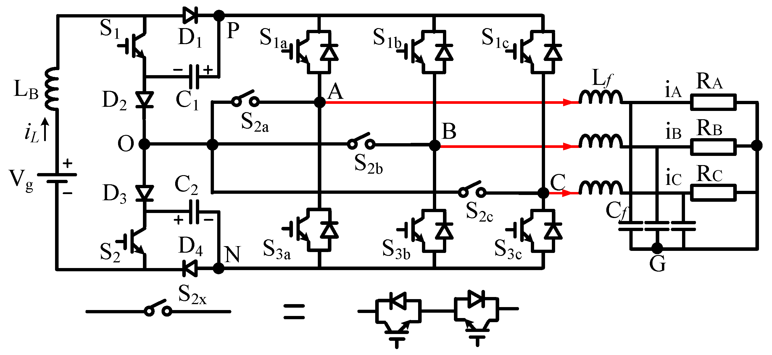
2I is illustrated in
Figure 1, where the intermediate qSB network is placed in front of the 3LT
2I. The qSB network is constructed by one inductor (
LB), two capacitors (
C1 and
C2), two active switches (
S1 and
S2), and four diodes (
D1,
D2,
D3, and
D4). A three-phase low-pass filter which consists of
Lf and
Cf is used to reduce total harmonic distortion (THD) at the output. The connection of two identical qSB creates the neutral point “
O” connected to load through three bi-directional switches, which consist of two active switches connected in series, shown in
Figure 1. This topology provides superior advantages in medium and low application compared to conventional topology of MLIs because these bi-directional switches block only half of the DC-link voltage. Moreover, the high side switches (
S1x,
x =
a,
b,
c) and low side switches (
S3x) are used to connect the positive point “
P” and negative point “
N” of qSB network outputs to the load, while the middle switches (
S2x) is connected to point “
0” of the qSB network to the load, as shown in
Figure 1. By this example, the inverter leg can produce three-level voltages at the output terminal as “
P”, “
O”, and “
N”, which ensure the advantages of MLIs. Moreover, by using the qSB network, this topology can behave as a boost converter which is able to generate desired AC output voltage at the load.
Like [
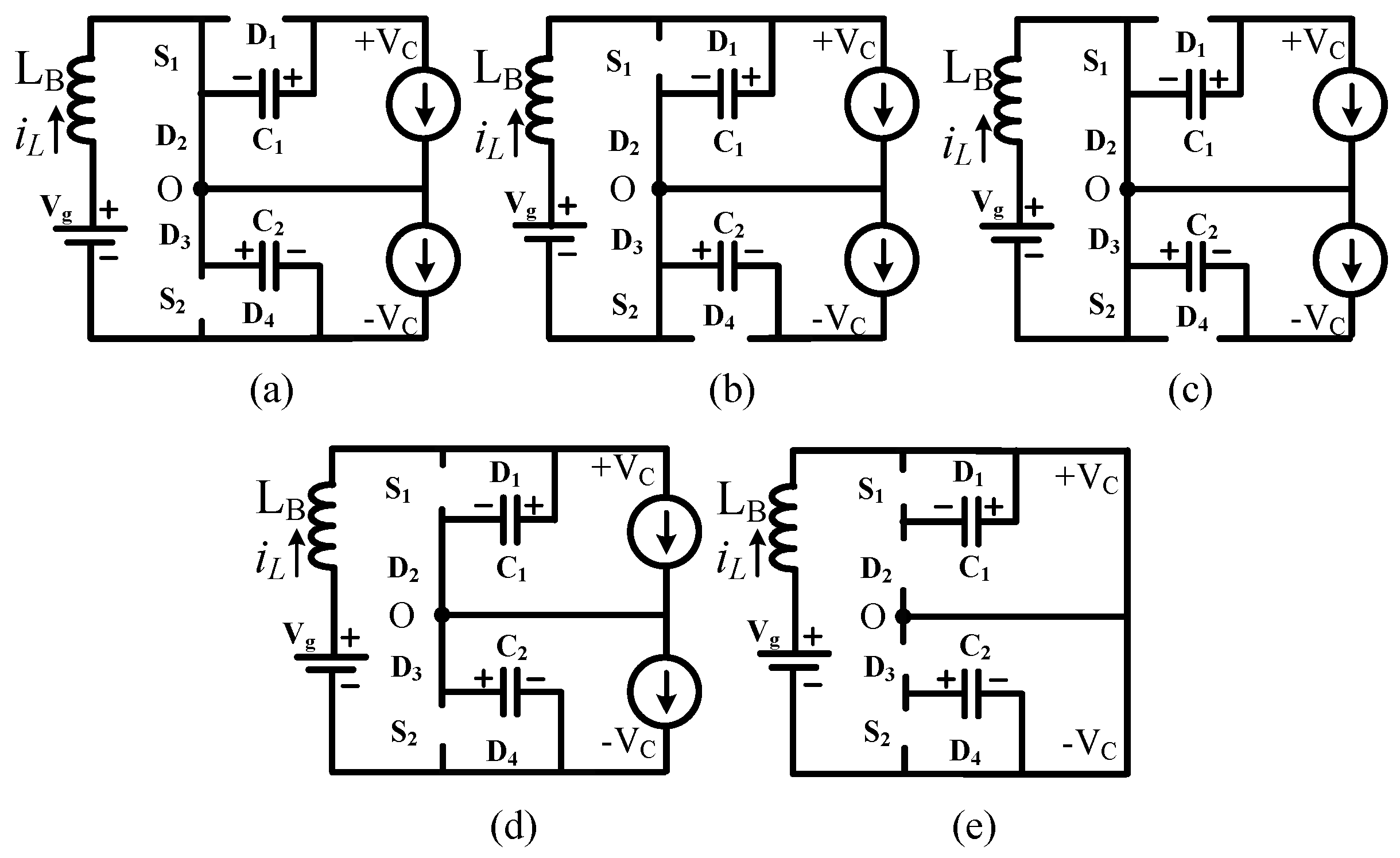
27], the inverter topology can operate in two main modes: ST and NST, which consist of four sub-NST modes as illustrated in
Figure 2. As presented in
Figure 2a, inductor
LB stores energy in NST mode 3 by switching both switches
S1 and
S2, where the inverter leg operates normally by producing three-level voltages at output. On the other hand, the inductor is also charged by turning on all switches of the inverter leg in ST mode, which produces “O” state at output terminal. Therefore, the ST state is considered to insert within “O” state in order to not affect the normal operation of the converter. Due to the use of ST state, the efficiency and reliability of the system are improved, which are not guaranteed in a conventional inverter when the deadtime is included in switching control signal. In NST mode, the inverter operates similar to conventional MLIs, which is able to achieve three-level at output terminal, the energy stored in inductor and power source is transferred to the load by triggering the corresponding switches, as detailed in
Table 1.
The steady state is processed in the same condition compared to [
27] in which the qSB network is considered symmetrical (
C1 =
C2) and the voltage across these capacitors is assumed constant (
VC1 =
VC2). As a result, the capacitor voltage is expressed as (1).
where,
VC1, VC2—capacitor voltage of C1 and C2;
Vg—input DC voltage of the inverter;
D0—ST duty ratio;
d—the ratio identifying duty cycle of intermediate network switches (S1 and S2).
The relationship between ST duty ratio
D0 and the ratio
d is shown in (2).
When applying the ST algorithm presented in [
27], the inductor current ripple of qSBT
2I can be decreased compared with the qZS network. As a result, the performance of the system is significantly improved. The value of inductor current ripple is expressed as follows:
where,
—the inductor current ripple;
LB—the value of the boost inductor;
fC—the frequency of the carrier.
The RMS value of output voltage can be identified through capacitor voltage and calculated as [
27]
where,
In order to avoid affecting the output voltage, the relationship between modulation index
m and ST duty cycle
D0 must be
3. The Proposed SVM Scheme to Eliminate CMV for 3L qSBT2I
During operation, the MLIs generate CMV, which is identified as the voltage between load neutral point “
G” and DC-link neutral point “
O”. It can be calculated through three-phase output voltage and the CMV, as presented in (6).
where
VAO, VBO, and
VCO are three-phase output pole voltages.
There are 27 vectors corresponding to 27 switching states of the 3LT
2I. The CMV value is produced according to the vector adopted to generate the output voltage.
Table 2 lists the CMV value of 3LT
2I.
As illustrated in
Table 2, the maximum magnitude of CMV is reached when the zero vectors [PPP] or [NNN] are adopted, its value is ±
VC. When small vectors are adopted to synthesize the reference vector, the CMV value is changed from −2
VC/3 to +2
VC/3, while the large vectors just generate the CMV whose peak value is
VC/3. Along with 27 vectors listed in
Table 2, the zero vector [OOO] and medium vectors generate the CMV with the minimum value, which is zero. Therefore, when zero vector [OOO] and medium vectors are adopted to create the output voltage, the CMV is eliminated.
This paper proposes a SVM strategy by using the medium vectors and zero vector [OOO], which synthesize the reference vector applied to qSBT
2I. As a result, CMV will be eliminated. The space vector diagram is illustrated in
Figure 3, where the magnitude of medium vectors and zero vector [OOO] are
and 0, respectively. The maximum magnitude of reference vector is
VC. The space vector diagram is divided into six sectors, which is used to analyze the operation principle of the inverter. During operation, the ST state is added into zero vector in order to avoid affecting the output voltage and provide a boost capability. The drew-time calculation, switching sequence, and ST insertion are presented in this section. Generally, the sector I is considered as a representative instant to analysis. The calculation for other sectors can be achieved in a way similar to the sector I.
Assume that the reference vector is located in the sector I, the medium vectors (
and zero vector
are adopted to synthesize the reference vector. Their relationship will be presented in (7).
where,
—reference vector;
—zero vector;
—medium vectors;
Ts—switching period of the inverter;
T0, T1, T2—the on-times of , and , respectively.
The reference vector
, zero vector
, and medium vector
are identified as follows:
where
m is the modulation index.
Based on (7) and (8), the drew time of these vectors can be calculated as follows:
The switching sequence for sector I is [OOO]-[PON]-[PNO]-[OOO]-[PNO]-[PON]-[OOO].
When the ST state is obtained, all switches of the inverter leg are turned on at the same time. As a result, the output voltage is zero, which is similar to zero vector [OOO]. Therefore, to guarantee the boost capability of the qSB network and to not affect the output voltage, the ST vector is added into zero vector, so the zero vector is changed as
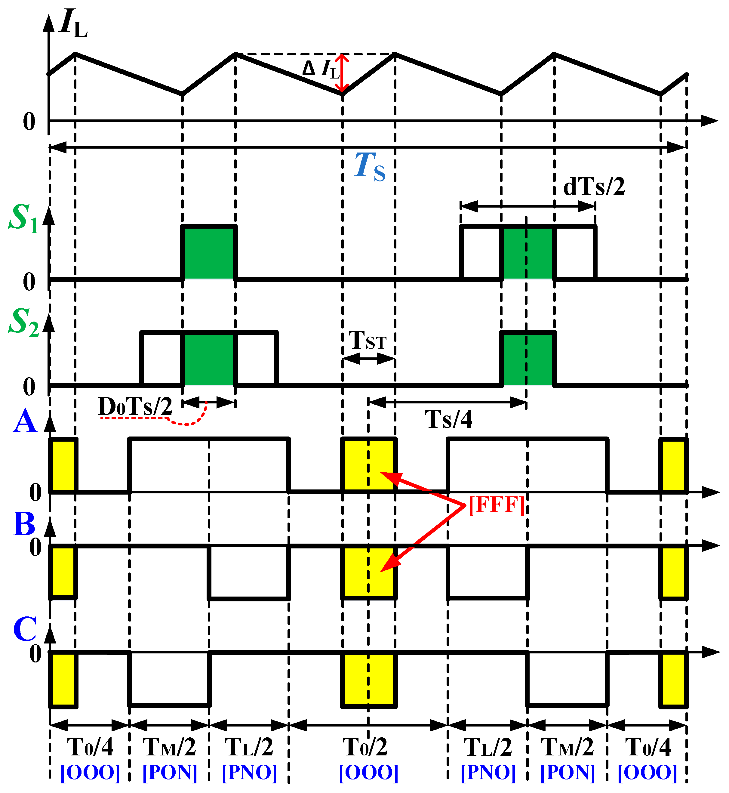
By incorporating the ST state with the switching sequence mentioned above, the designed switching sequence is changed to [FFF]-[OOO]-[PON]-[PNO]-[OOO]-[FFF]-[OOO]-[PNO]-[PON]-[OOO]-[FFF], where [FFF] is ST vector. For more details, ST insertion and control signals of intermediate network switches (
S1 and
S2) are presented in
Figure 4. The ST control signal of impedance network, which has the phase shift of 90° compared to ST of the inverter leg, is generated to ensure the advantage in reducing the inductor current ripple. Moreover, by adding more duty cycle for switching
S1 and
S2 (which is represented by dT
S/2 in
Figure 4), the voltage gain of the converter is further enhanced.
Similar to the sector I, the switching sequence of other sectors and ST insertion can be achieved in the same way, as presented in
Table 3.
4. Simulation and Experimental Results
The effectiveness of the proposed SVPWM is verified with the help of PSIM and a practical prototype. The circuit parameters used in the simulation and the experiment are shown in
Table 4.
Three PWM techniques are considered to use in the simulation and the experiment to validate the performance of this research: method 1—traditional phase disposition (PD) sinusoidal PWM scheme, method 2—traditional phase shift (PS) sinusoidal PWM scheme discussed in [
30,
31], method 3proposed scheme. The results of method 1 are achieved by applying the ST insertion method, which is used in UST and LST insertion explored in [
29,
30], to conventional PD sinusoidal PWM strategy.
When using modulation index as 0.8 and ST duty ratio as 0.2, as illustrated in
Table 4, the
d ratio is calculated as 0.63 to achieve 110
VRMS at output phase voltage from 150 V at the input power supply.
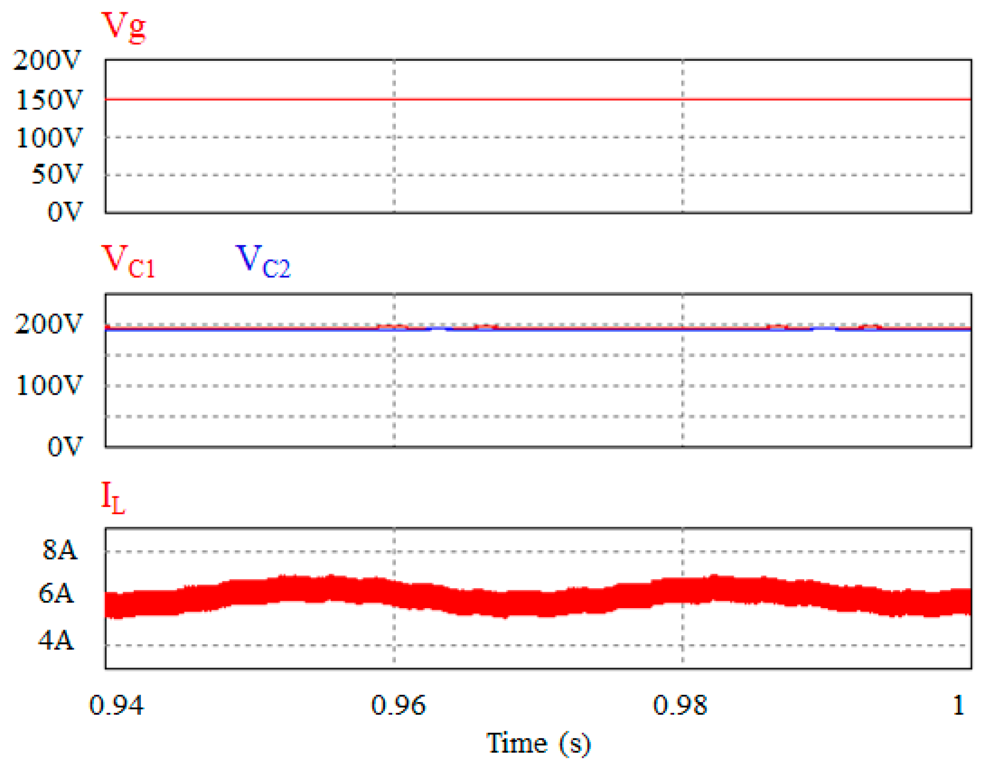
Figure 5 presents the simulation results about input voltage (
Vg), capacitor voltages (
VC1 and
VC2), and inductor current (
IL) of the proposed method. The simulation is conducted with the parameters listed in
Table 4. As a result, the capacitor voltage is boosted to 194.8 V in theory, and the simulation measures 196 V and 193 V for
C1 and
C2, respectively. The peak value of the DC-link voltage is the sum of two voltages across capacitors. Therefore, it is 389 V in simulation. The average input current (also inductor current) in simulation is 6.1 A, as shown in
Figure 5. In one period of output load voltage, the maximum and minimum values of the inductor current are 7 A and 5.2 A, respectively.
Figure 6 illustrates the simulation results of the DC-link voltage, phase voltage (
VAG), and CMV in three PWM techniques mentioned above. Among these techniques, the peak-value of the DC-link voltage is similar, which is 389 V. Because of using UST and LST, the DC-link voltage of method 1 varies from V
DC-link/2 to V
DC-link, while the DC-link voltage of method 2 and the proposed method has two values, which are 0V and V
DC-link, since they use full ST to boost the DC power source. As shown in
Figure 6, the THD value of the phase voltage is increasing from method 1 to the proposed method. The simulation produces results of 42.07%, 67.32%, and 77.08% for THD values of method 1, method 2, and the proposed method, respectively, while the CMV value of method 1 has the maximum magnitude, which is 2
VC/3 and equals to 130 V. Method 2 has the medium magnitude of CMV, which varies from +
VC/3 (65 V) to −
VC/3 (–65 V). When the proposed method is adopted, the CMV generated by qSBT
2I is eliminated. The RMS values of CMV for the three methods are 71
VRMS, 41.6
VRMS, and 0
VRMS, respectively. Since CMV is eliminated, the output phase voltage is similar to the pole voltage, which just has three-level +
VC, 0, and –
VC, as shown in
Figure 6c.
Figure 7 shows the simulation results of output line–line voltage (
VAB), output load voltage (
VRA), and output load current
IA. When the proposed method is used to minimize the effect of CMV, the THD of the output voltage is increased, consequently. In simulation, the THD value of output line–line voltage (
VAB) for three methods are 42%, 67.3%, and 77.1%, respectively. The magnitude of line–line voltage is equal to peak DC-link voltage, the variable of
VAB varies from 0 to 390 V at the top part, as illustrated in
Figure 7. Since this topology uses low pass filter (LC filter) at output, the THD value of output load current is very low, and they are 0.7%, 0.51%, and 1.28% for method 1, method 2, and the proposed method, respectively. The RMS value of output load voltage and output load current for three strategies are similar, which are 110
VRMS and 2.77
ARMS.
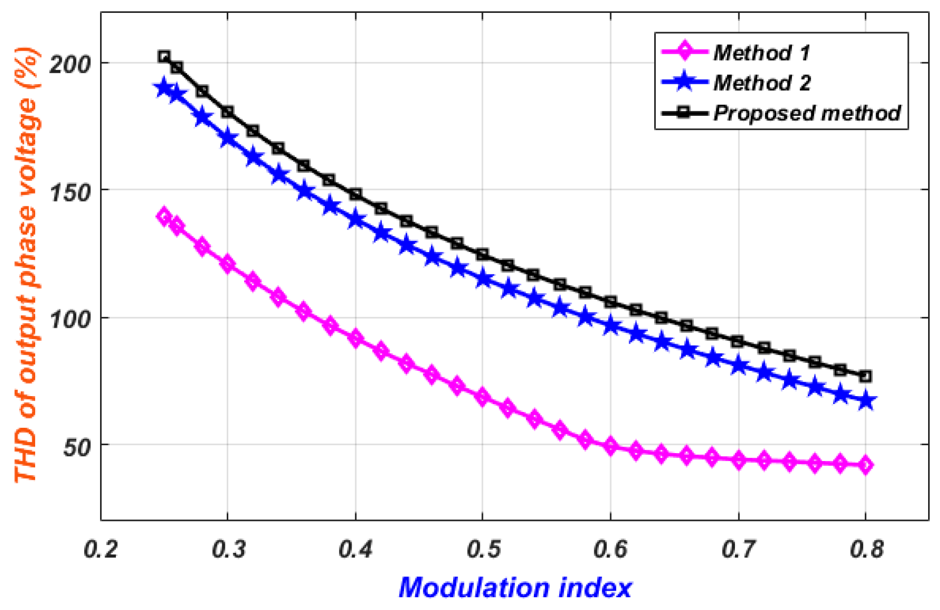
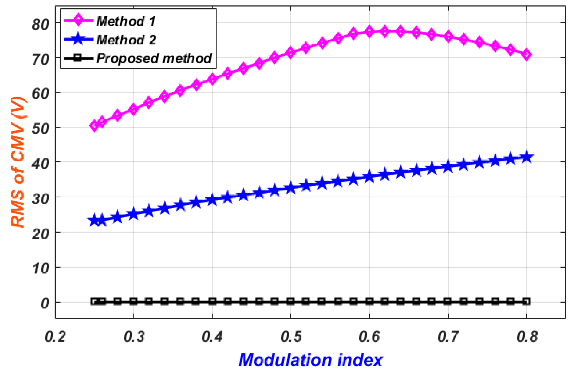
The THD value of output phase voltage (
VAG) and RMS value of the CMV investigated under difference modulation indexes are performed in the simulation. The value of the modulation index (
m) varies from 0.25 to 0.8, whereas the ST duty ratio is kept constant. The results are shown in
Figure 8 and
Figure 9, respectively. As illustrated in
Figure 8, by increasing the value of the modulation index, the quality of output phase voltage is improved, which is illustrated through the decrease of the THD value.
Figure 8 presents that method 1 is superior in THD, because of using small vectors [
34], which generates ±2
VC/3 of CMV, while the other two techniques have higher value of THD, and the difference is not too large.
Figure 9 shows the results of investigating the RMS value of CMV. Method 1 has the maximum value of CMV, which achieves the maximum value of RMS CMV at 0.6 of the modulation index. The RMS CMV value generated by the proposed method stays at zero when the value of modulation index changes, whereas in method 2, it is increased with the increase of modulation index.
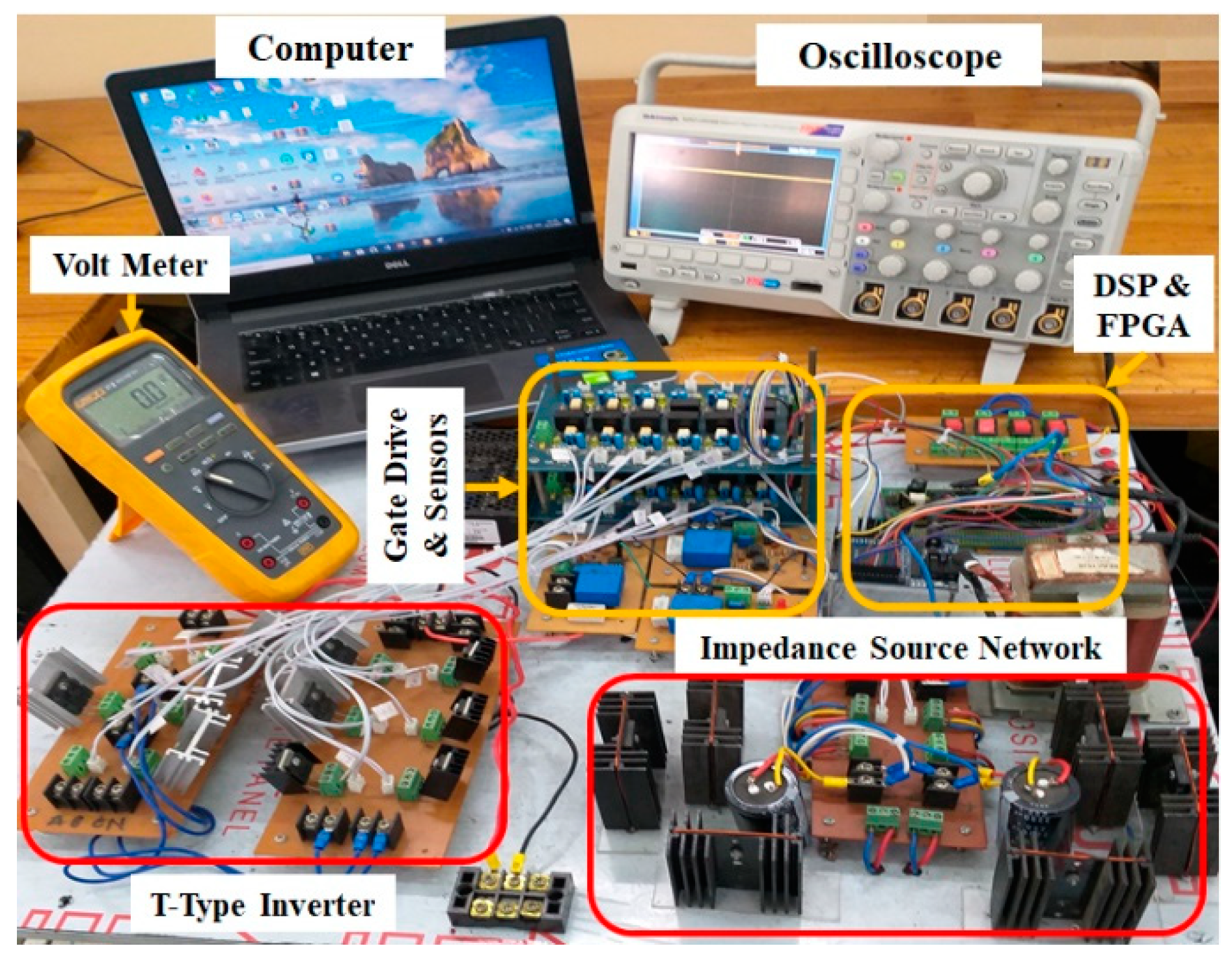
To demonstrate the performance of the proposed SVM method, a 1kW 3L qSBT
2I prototype was created based on DSP TMSF28335.
Figure 10 shows a photo of the hardware setup. Parameters of devices used in the experiment are listed in
Table 4. Diodes and IGBTs used in the experiment are DSE160-12A and FGL40N150D, respectively. The modulation index, ST duty ratio, and
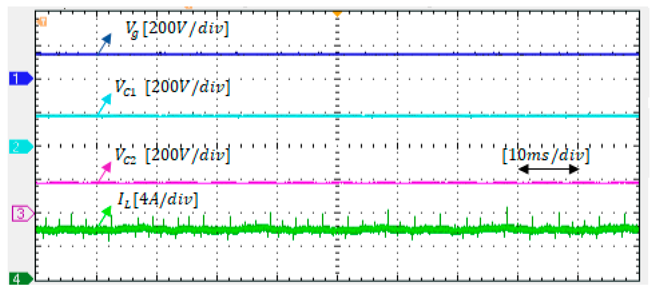
d are selected similar to the simulation. With the 150 V of the DC input voltage, the capacitor voltages are boosted to 187 V and 190 V corresponding to voltages across
C1 and across
C2. They are maintained during the operation of the system. The average value of inductor current measured in the experiment is 6.02 A, as shown in
Figure 11.
Figure 12 shows the experimental waveform results of the DC-link voltage, phase voltage (
VAG), and CMV of three methods. For method 1, presented in
Figure 12a, the variation of the DC-link voltage is from 190 to 380 V, approximately, because of using UST and LST to ensure the boost capability of the qSB network, while the DC-link voltage of the other two methods varies from 0 to 380 V by using FST insertion in order to boost the DC input voltage. Since CMV of the proposed method is eliminated, the output phase voltage has just three levels: –190 V, 0 V, and +190 V, approximately, as presented in
Figure 12c. Method 1 and method 2 have a higher number of level at output phase voltage, as illustrated in
Figure 12a,b, so the quality of their output voltage is improved compared to the proposed method. However, among the three techniques, the RMS CMV of the proposed method measured in the experiment is 5.73
VRMS, while it is 67.8
VRMS and 40.2
VRMS in method 1 and method 2, respectively. As a result, the CMV of the proposed method is reduced to 91.5% and 85.7% compared to method 1 and method 2, respectively.
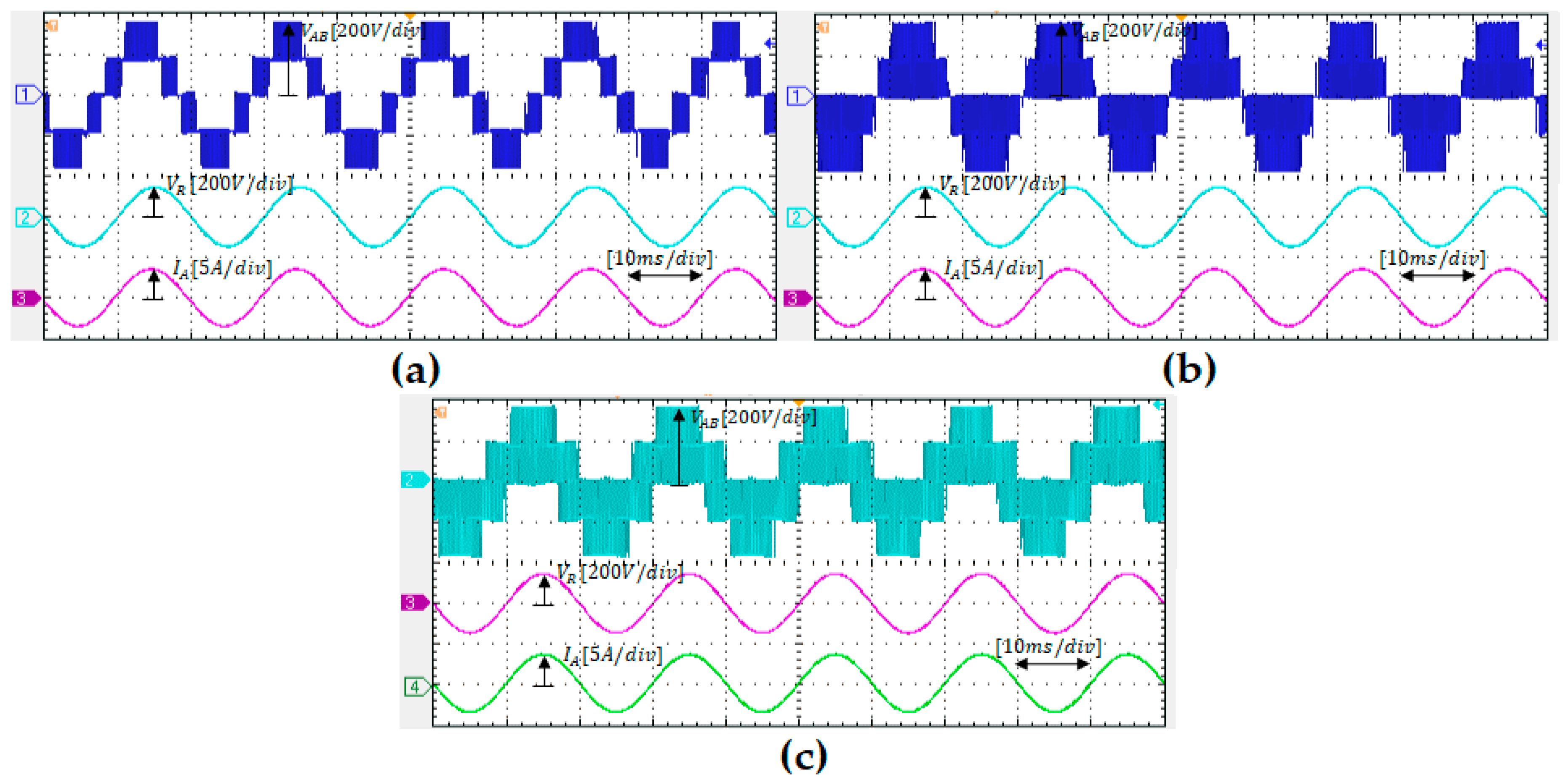
Figure 13 presents the experimental results of the output line–line voltage (
VAB), load voltage (
VRA), and output phase current (
IA) of three methods. Similar to the output phase voltage mentioned above, the output line–line voltage generated by the proposed method has the lowest quality because of just using medium vectors and zero vector to produce output voltage. The maximum magnitude of the output line–line voltage is the same as the magnitude of the DC-link, which is 380 V, approximately. By using the low pass filter at output, the amplitude of high frequency harmonic is reduced significantly. As a result, the output load voltage and output load current have less THD value, as shown in
Figure 13. The RMS value of output load voltage and current are the same when three methods are adopted, which are 105
VRMS, 104
VRMS, and 104
VRMS corresponding to method 1, 2, and the proposed method, respectively. The load currents are 2.6
ARMS, 2.58
ARMS, and 2.55
ARMS for the three methods.
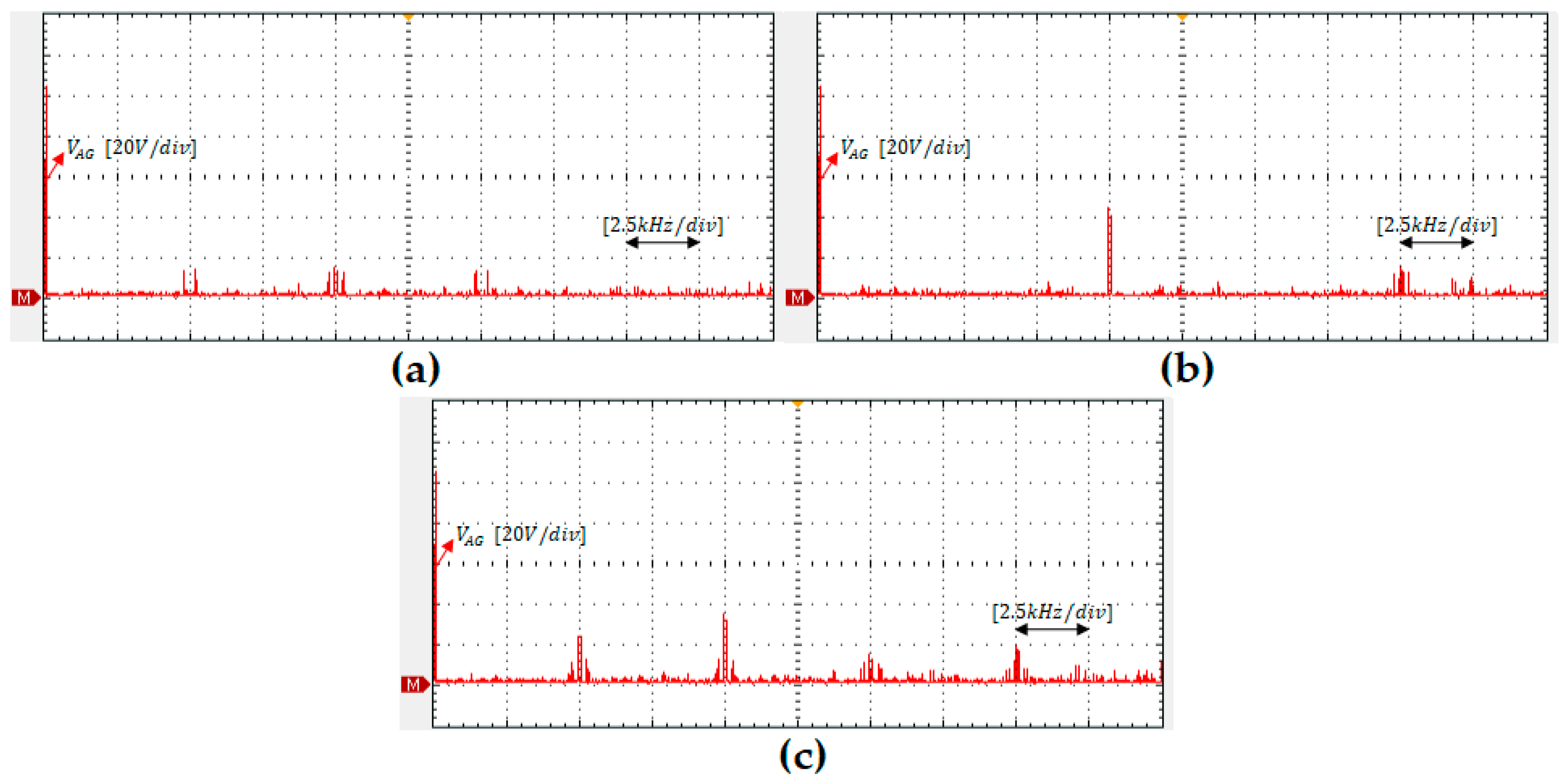
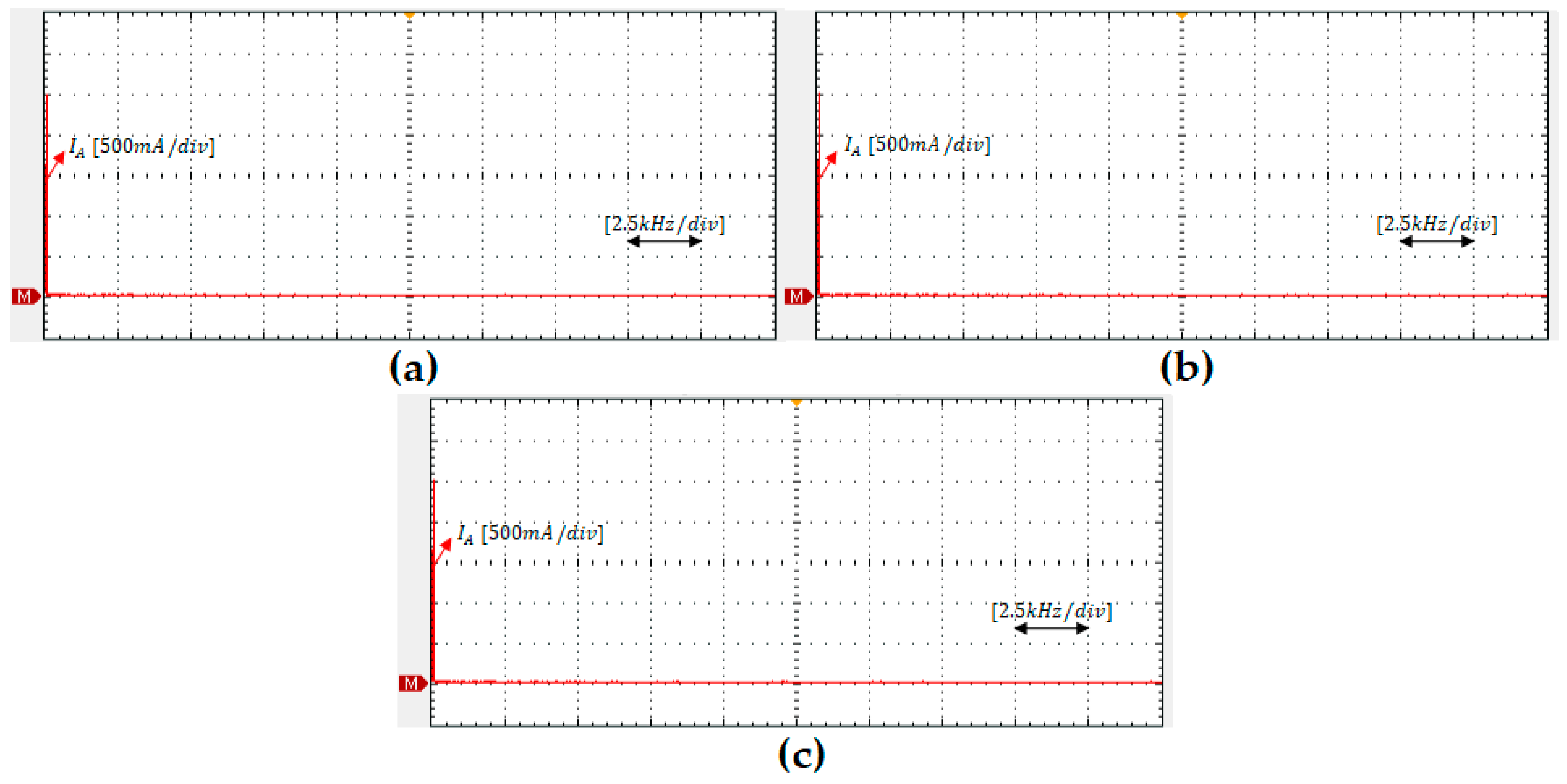
In
Figure 14 and
Figure 15, the FFT analyses of output phase voltage (
VAG) and output load current (
IA) are conducted accordingly for the three methods. Considering harmonics spectrums of
VAG and
IA, the magnitudes of first order harmonic of output load voltage and the output load current are the same for three methods, which are 104.5 V and 2.55 A. The THD values of
VAG and
IA are calculated by using results of harmonics spectrums, as shown in
Table 5. Among the three methods, the THD value of the proposed method is maximum, which is 89.18%, while it is 57.62% and 81.25% in method 1 and method 2, respectively. Because of appearing three-phase low pass filter at output, the THD value of load current is quite smaller than output phase voltage. They are 2.62%, 2.34%, and 3.3% corresponding to method 1, method 2, and proposed method.
