Abstract
This paper presents the design and modeling of a two-phase resonant converter that drives a LED lamp with a high-frequency pulsed current free of instabilities and flicker effect, fulfilling the recommendations of the IEEE PAR 1789-2015, so that it enables visible light-based communication at a 10 kB/s bit rate. The dynamic study of the converter takes into consideration the effect of the reflected impedance of the output filter on the AC side. In order to evaluate the dynamic response of the converter, a Spice model is defined. A 120 W prototype intended for street lighting applications has been built to validate the analysis and modeling.
1. Introduction
Solid state lighting (SSL) is the most recent revolution in the lighting field [1], which paves the way to developing new capabilities such as a precise wide-range dimming and visible light communication (VLC), compatible with the illumination service. High-performance dimming is highly desirable to achieve energy savings. LEDs’ operation at their nominal current prevents the degradation of light quality parameters [2]. For this reason, dimming or turning on/off the nominal current level through the LEDs, according to a PWM pattern, modifying the average current, is preferred over the current amplitude modulation. A fast response of the LED current controller is required to achieve PWM dimming operation free of any flicker perception. Recently, the IEEE PAR1789 recommended a minimum frequency of 1250 Hz to implement PWM dimming [3]. Moreover, a fast dynamic response of the LED driver also enables the communication by light pulses, which is an interesting feature for positioning autonomous vehicles, home automation solutions, and management of lighting systems [4,5], among other applications [6]. This paper focuses on the analysis of the dynamic response of a phase-controlled series-parallel resonant converter, designed as a current source, for LED lamp driver applications. Different models have been proposed to study the dynamic response [7] of resonant converters. The small-signal modeling of resonant converters is a complex task, taking into account the number of reactive elements and operation modes. This work proposes a reduced-order model of the converter, which is valid at the bandwidth of interest. The model is defined in the LT-Spice environment providing technical insight and better understanding of the circuit. The effect of the reflected impedance of the output filter on the AC side is analyzed and then included in the model.
The paper is organized as follows: Section 2 presents the inverter and rectifier sections of the two-phase series-parallel resonant converter, deriving an equivalent circuit and the phase modulation principle using the fundamental approximation. In Section 3, the reduced small-signal model is obtained from the envelope model of the converter. The experimental validation of the model is presented in Section 4, finalizing with the discussion of the results.
2. Two-Phase Series-Parallel Resonant Converter
The two-phase series-parallel (LCsCp) resonant converter [8], shown in Figure 1, consists of the resonant inverter stage loaded by a center tap rectifier [9].
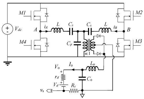
Figure 1.
Two-phase LCsCp resonant converter.
The transformer with turns-ratio n:1 provides galvanic isolation. The shunt resistor Rs is the sensor of the lamp current. The LED lamp is modeled with the dynamic resistance, rd, and the junction voltage drop Vd, i.e., a linear model of the diode.
2.1. The LCsCp Resonant Inverter Stage
In steady state, the center tap rectifier is first modeled by an equivalent resistance Rac on the AC side. The Fundamental Harmonic Approximation (FHA) [9] is then applied to obtain a large signal analysis of the circuit.
The midpoint voltages va and vb in Figure 2 are represented in the complex domain by their exponential forms,
where Ψ is the phase displacement between va and vb. The circuit in Figure 2 exhibits a symmetrical structure, where the ground-connected load can be decomposed into two paralleled halves, 2Rac, along the symmetry axis [8]. Decomposing VA and VB into their orthogonal components, it is observed that the imaginary parts have equal amplitude and 180° phase displacement. Therefore, according to the symmetric structure of the circuit, they cancel each other out,
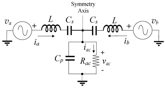
Figure 2.
Simplified circuit for steady-state analysis purposes.
The resonant inverter is reduced to the equivalent circuit shown in Figure 3, where the input voltage, VAB, is the sum of the real part of VA and VB, i.e., the common-mode voltage.

Figure 3.
Two-phase LCsCp resonant inverter. Circuit simplified according to the Bisection Theorem.
The parallel parameters of the LCsCp inverter are summarized in Table 1.

Table 1.
Parallel parameters of the LCsCp resonant inverter.
From the circuit in Figure 3, the phasor of the output current on the AC side of the converter is obtained,
Since LEDs are current-driven devices, current source behavior of the driver circuit is highly desirable. For the LCsCp resonant inverter, the current source behavior is achieved by fixing the switching frequency at ω = Ωo,
Working at Ωo, it is possible to achieve the zero voltage switching (ZVS) mode of the transistors of the converter, minimizing the switching loss. Upon substitution of (4) into (3), it can be verified that the phasor of the output current on the AC side has no dependence on the load, while it is modulated with Ψ.
2.2. Center Tap Rectifier
Next, Rac for the model and the LED current, Io, are calculated. The center tap rectifier with an LC filter at the output is shown in Figure 4, where ro includes both the dynamic resistance of the LED lamp, rd, and the shunt resistor, Rs, so that, ro = rd + Rs. The rectifier stage removes the high-frequency ripple generated by the operation of the inverter. Under this consideration, the low ripple approximation is used [9]. Thus, the rectifier section is modeled at low frequency by its averaged variables.
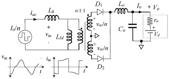
Figure 4.
Center tap rectifier.
Taking into account that the rectifier and filter impose a square waveform for the current on the primary side of the transformer [9], the first harmonic of the square waveform is used to obtain the relationship between the amplitude of the AC side current, Îac, and the DC side current, Io,
On the other hand, the output voltage, Vo, is the voltage across the LED lamp and the shunt resistor Rs. Carrying out the power balance between the AC and DC sides of the converter, Vo is obtained,
From (7) and (8), the large-signal lamp model is represented on the AC side by,
From (9), the impedance seen from the AC side in steady-state, Rac, is:
Since the LED lamp is connected on the DC side, working with (5) and (6), the DC output current is obtained as a function of the inverter parameters:
From (10), (5) and Figure 1, it can be observed that the proposed converter enables control of the LED lamp current by adjusting the phase displacement angle, Ψ, between the midpoint voltages va and vb. In this approach, the switching frequency of the converter is constant at Ωo, which simplifies the control circuit and optimizes the magnetic components’ design.
3. Envelope Model of the Resonant Inverter Stage
Low-frequency perturbations cause the modulation of voltage and current waveforms in the resonant circuit [10]. Assuming the FHA, the general form of any modulated waveform is given in (11),
Given that the control of the converter is performed at constant switching frequency, the variation of the control parameter Ψ(t) results in the amplitude modulation of all the variables [10],
Using (12), the time-varying amplitude of the current and voltage phasors are defined with (13) and (14), assuming constant switching frequency, ω = Ωο,
Upon substitution of (13) and (14) into the equations of the inductor voltage and capacitor current, the envelope model of the resonant circuit components is obtained [8].
From (15) and (16), it can be seen that the envelope model of the reactive components incorporates an imaginary resistor [11]. The imaginary resistor represents the steady-state impedance of the corresponding reactive element at the switching frequency.
The input voltage to the resonant circuit is obtained considering that the control angle, Ψ(t), is time-dependent, and it modulates the amplitude of the input voltage.
Therefore, the voltage source applied to the envelope model is given by,
Finally, applying (15), (16) and (18) to the circuit of Figure 3, the envelope model of the LCsCp resonant inverter stage is obtained,
Observing Figure 5, it is possible to reduce the order of the model by assuming that the switching frequency Ωo is much higher than the frequency of any perturbation. In this way, L and Cs along with the associated imaginary resistances can be lumped in an equivalent inductor in series connection with the steady-state Cs impedance as shown next,
where, ωs is the resonant frequency of the series branch L-Cs.
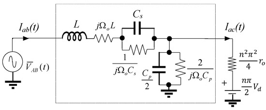
Figure 5.
Large-signal envelope model of the inverter stage.
Then, after grouping terms, the envelope model of the series branch is further reduced to the equivalent inductance, Lrd, in series with an imaginary resistor, jXrd, defined as follows:
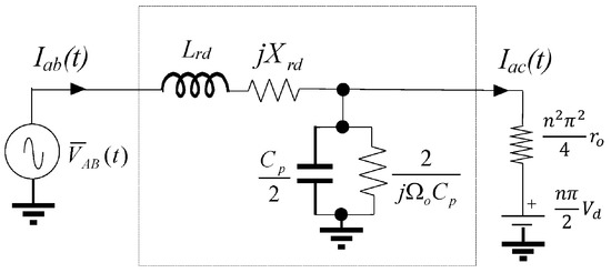
Figure 6.
Large-signal reduced-order envelope model of the inverter stage.
It should be noted that the reduced-order model incorporates the main dynamic effect of the capacitance Cs at low frequency, which is expressed by the new inductance Lrd.
3.1. Real and Imaginary Subcircuits in the Model
According to the procedure explained in [11], the complex circuit in Figure 5 and Figure 6 can be simulated with Spice if the circuit is split into its real and imaginary parts. The corresponding real and imaginary subcircuits are shown in Figure 7 and Figure 8 respectively. Voltages and currents are obtained by composing the ones in the real and imaginary circuit, e.g., Iac. This method is also used for the analysis.
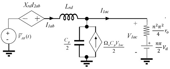
Figure 7.
Real part of the large-signal reduced-order envelope model of the inverter stage.
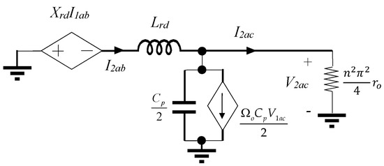
Figure 8.
Imaginary part of the large-signal reduced-order envelope model of the inverter stage.
The envelope of the output current on the AC side is calculated composing its orthogonal components.
Once the envelope of the output current on the AC side is obtained, the calculation of the DC output current is straightforward applying (6) as represented in Figure 9.
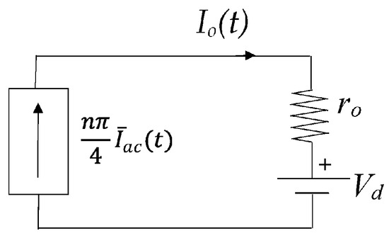
Figure 9.
DC output current obtained from the envelope of the AC side output current.
3.2. Small-Signal Envelope Model
Perturbing and linearizing (23), the small-signal component of the AC side load current envelope is obtained,
In (24), î1ac and î2ac are the small-signal components of I1ac and I2ac. Solving the circuits in Figure 7 and Figure 8, the steady-state components of the output current, I1ac and I2ac, are obtained. From (5), at frequency Ωo where the inverter behaves as a current source, the phasor of the steady-state output current is purely imaginary, i.e., I1ac = 0 and, therefore, Iac = I2ac, so that,
The small-signal current obtained in (25) is applied to the input impedance of the loaded output filter, zif, as shown in Figure 10.
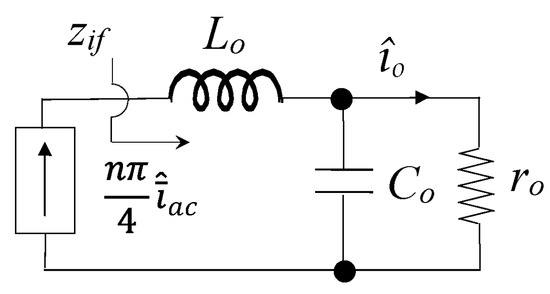
Figure 10.
Small-signal response of the output current.
In order to obtain the linear small-signal plant of the resonant inverter, the modulation signal, Ψ, has to be perturbed [11], which results in perturbation of the input voltage. Then, the small-signal perturbation, ϕ, is added to Ψ:
Substituting (26) into (17) and extracting the small-signal component,
The AC side small-signal load impedance is the input impedance of the output filter reflected on the AC side,
The resulting small-signal reduced-order model of the phase-controlled LCsCp resonant converter is shown in Figure 11.
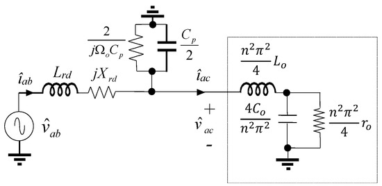
Figure 11.
Small signal of the reduced-order envelope model of the AC side.
Splitting the model of Figure 11 into real and imaginary sub-circuits, the small-signal components î1ac and î2ac are calculated. Upon substitution of î2ac into (25), the control-to-output current transfer function in the AC side is obtained.
4. Experimental Results
The experimental prototype and lamp setup are shown in Figure 12.
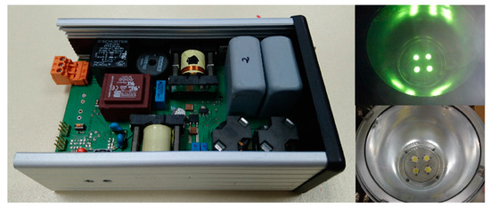
Figure 12.
Experimental prototype and lamp composed of four LED arrays BXRA-C2000. Case size is 16 cm × 10 cm × 5 cm.
The lamp consists of four BXRA-C2000 LED arrays in series connection with a nominal current Io = 1.75 A, output power Po = 120 W, output voltage Vo = 68.6 V and equivalent DC load, and Ro = 39.2 Ω. The control angle under nominal conditions is Ψo = 45°, which provides full control capability. The input DC voltage is Vdc = 400 V. The transformer’s turns ratio is chosen to be n = 2, which implies that Rac = 193.4 Ω. The capacitor ratio is Cp/Cs = 0.1.
After collecting all the input data, the step-by-step design sequence of the converter is as follows: Upon substitution of n, Vdc, Ψo and Io into (10), the characteristic impedance is obtained, Zp = 433 Ω. From Table 1, the parallel quality factor is Qp = 0.894. The resulting value of the quality factor produces 48° phase lag of the current referred to the voltage in the transistors, which is enough for ensuring the ZVS mode under all operating conditions. The switching frequency is set at Ωo = 2π (100 kHz). From (4), the parallel resonant frequency is ωp = 2π (97.6 kHz). Finally, the reactive components are L = 705 µH, Cp = 7.5 nF and Cs = 75 nF. The output filter components are Lo = 150 µH and Co = 3.3 µF. The use of electrolytic capacitors, even in the power factor correction stage, is avoided in order to achieve high circuit reliability [12]. The resonant inverter stage was implemented using IRF840LC MOSFET transistors. The resonant inductors were built using the ferrite core RM10 of material 3C90. The experimental lamp current and voltage under nominal conditions are shown in Figure 13, where PhA and PhB are the signals for driving phases A and B of the converter.
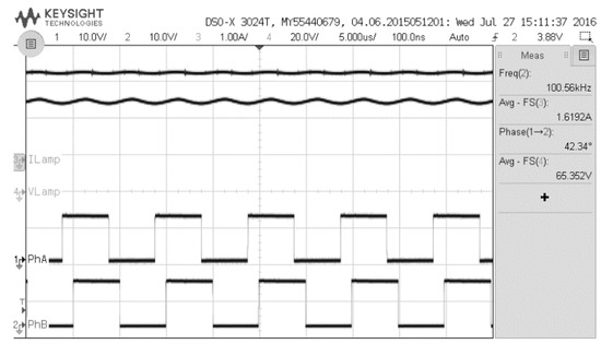
Figure 13.
Lamp current, lamp voltage and control signals in steady state.
From Figure 13, the driver performance under nominal conditions can be verified. The current of the LED lamp is Io = 1.62 A. The phase displacement angle, Ψ, between the drive signals PhA and PhB is Ψ = 42.3°. The efficiency of the proposed driver is 92%.
4.1. Validation of the Converter Dynamic Model
The core of the control circuit is a phase modulator [13], which is implemented using a sawtooth carrier (leading edge) signal, a comparator and two monostable multivibrators. The control voltage, vc, and the carrier are compared, generating a PWM signal that triggers the drive signals of phases A and B of the converter. The waveforms are shown in Figure 14.
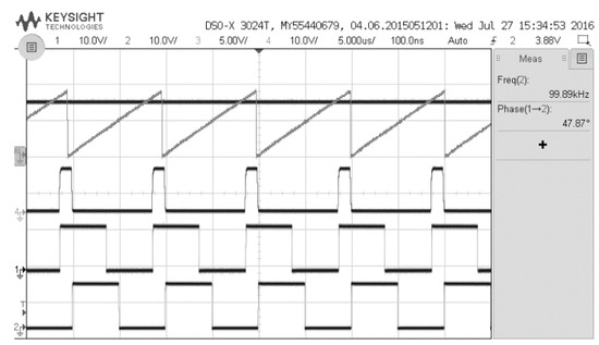
Figure 14.
Waveforms of the phase modulator for Ψ = 45°. From top to bottom: Sawtooth carrier signal. Control signal, vc. Pulsewidth modulated signal. Drive signals applied to the resonant converter branches.
The LT-Spice description of the real and imaginary sub-circuits of the small-signal model are shown in Figure 15. The dynamic resistance of the LED lamp is rd = 5 Ω. The shunt resistor is Rs = 0.5 Ω, so the dynamic output resistance is ro = 5.5 Ω. The ESR of the output filter components is considered. The input voltage for the AC simulation of the model is defined by (27), taking into account that the gain of the phase modulator is Gϕ= −0.7 rad/V, and the amplitude of the perturbation is vc = 500 mV.
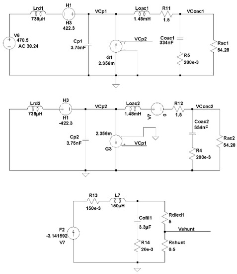
Figure 15.
LT-Spice implementation of the small-signal model of the resonant converter.
The open-loop control-to-output current AC characterization, shown in Figure 16, has been carried out injecting a constant amplitude perturbation signal, vc = 0.5 V, between 51.2 Hz and 51.2 kHz, using an Agilent 35670A Dynamic Signal Analyzer. From Figure 16, it can be observed that the proposed model and the experimental results are in good agreement up to 30 kHz, verifying a first-order dominant behavior of the resonant converter.
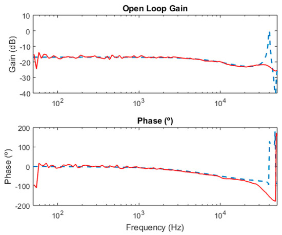
Figure 16.
Experimental (solid red line) and predicted by the proposed model (dashed blue line) AC response of the converter.
The experimental bandwidth ωH = 2π (9 kHz) is wide enough to implement the PWM dimming at a frequency fPWM = 2 kHz, which exceeds the recommendation regarding the minimum frequency for avoiding flicker perception given by the IEEE PAR 1789. The result is in good agreement with (29).
The reflected impedance of the output filter on the AC side produces a peak of resonance, whose position is given by,
In order to preserve the first-order behavior of the converter and achieve wide bandwidth, the converter should be designed to fulfill ωH < ωf.
4.2. PWM Control of the Lamp Current
As stated previously, the converter enables the implementation of the PWM control of the lamp current. The off-time is achieved by imposing Ψ = 180°. A good feature of the phase-shifted mode PWM is that the resonant tank is not fully discharged, which prevents uncontrolled on/off transient oscillations of the converter variables. The experimental waveform for 50% dimmed operation is shown in Figure 17. The current during the on-time is the nominal one of the LED lamp, Io = 1.7 A, which assures the quality of the light, without any chromatic modification. The average current of the lamp is 0.86 A, and the power is 59 W, verifying the operation at 50% of the nominal power. The efficiency of the proposed driver, measured at 50% of the nominal current, is 87%.
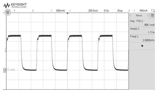
Figure 17.
Experimental current of the lamp at 50% dimmed operation achieved by the phase-shifted PWM.
The converter bandwidth, close to 10 kHz, also enables data transmission, as is shown in Figure 18. The bit rate depends on the bit codification. For example, a light-based Amplitude-Shift Keying ASK modulation with an on-off keying codification can be implemented by switching the lamp current between two levels, as is shown in Figure 18. This on-off keying codification achieves a bit rate that is twice the frequency of the signal as two bits are transmitted during a cycle of the signal. In order to achieve the minimum degradation of the light quality during data transmission, the level of “1” and “0” were fixed at 1.7 A and 1 A, respectively. At these levels, the average current of the lamp is 1.3 A and the power is 92 W, close to the nominal conditions. During data transmission, the efficiency of the driver is approximately equal to the value under nominal conditions.
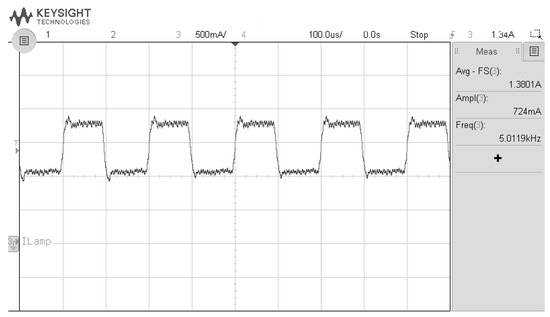
Figure 18.
Bi-level modulation of the lamp current for implementing data transmission at 10 kB/s.
5. Discussion
The small-signal model obtained from the reduced envelope model of the two-phase phase-shift-modulated LCsCp resonant converter, proposed as a driver for high-power LED lamps, has been validated with simulation and experimentally up to tens of kHz frequency. The output filter after the rectifier stage imposes on the converter control-to-output dominant single pole, so that a simple adjustment of the output capacitance in consistency with the load is enough to meet the IEEE PAR 1789 recommendations to perform wide-range PWM dimming, preventing any flicker perception, and to implement a VLC protocol using multilevel modulation. Experimental results show a ASK modulation capability up to 10 kB/s. Since no excessive variation of the resonant tank energy occurs during the phase-shift modulation transients, sharp amplitude modulation transients with no significant over-shoots or oscillations are achieved.
Author Contributions
Conceptualization, C.B. and F.J.A.; methodology, C.B.; validation, C.B., R.C. and F.J.D.; formal analysis, C.B.; investigation, C.B. and F.J.A.; writing—original draft preparation, C.B.; writing—review and editing, R.C. and F.J.D.; visualization, C.B.; supervision, F.J.A.; project administration, C.B. and F.J.A.; funding acquisition, F.J.A. All authors have read and agreed to the published version of the manuscript.
Funding
This work has been sponsored by the Spanish Ministry of Science and Innovation and the EU through the projects CICYT-FEDER-TEC2014-52316-R: “Estimation and Optimal Control for Energy Conversion with Digital Devices, ECOTRENDD” and RTI2018-095138-B-C31: “Power Electronics for the Grid and Industry Applications”.
Conflicts of Interest
The authors declare no conflict of interest.
References
- Crawford, M. LEDs for Solid-State Lighting: Performance Challenges and Recent Advances. IEEE J. Sel. Top. Quantum Electron. 2009, 15, 1028–1040. [Google Scholar] [CrossRef]
- Loo, K.H.; Lai, Y.M.; Tan, S.-C.; Tse, C.K. On the Color Stability of Phosphor-converted White LEDs Under DC, PWM and Bilevel Drive. IEEE Trans. Power Electron. 2012, 27, 974–984. [Google Scholar] [CrossRef]
- Wilkins, A.; Veitch, J.; Lehman, B. LED lighting flicker and potential health concerns: IEEE standard PAR1789 update. In Proceedings of the 2010 IEEE Energy Conversion Congress and Exposition, Atlanta, GA, USA, 12–16 September 2010; pp. 171–178. [Google Scholar]
- Carli, R.; Dotoli, M.; Pellegrino, R. A decision-making tool for energy efficiency optimization of street lighting. Comput. Oper. Res. 2018, 96, 223–235. [Google Scholar] [CrossRef]
- Pandharipande, A.; Caicedo, D. Smart indoor lighting systems with luminaire-based sensing: A review of lighting control approaches. Energy Build. 2015, 104, 369–377. [Google Scholar] [CrossRef]
- O’Brien, D.C.; Zeng, L.; Le-Minh, H.; Faulkner, G.; Walewski, J.W.; Randel, S. Visible light communications: Challenges and possibilities. In Proceedings of the 2008 IEEE 19th International Symposium on Personal, Indoor and Mobile Radio Communications, Cannes, France, 15–18 September 2008. [Google Scholar]
- Zheng, S.; Czarkowski, D. Dynamics of a phase-controlled series-parallel resonant converter. In Proceedings of the 2002 IEEE International Symposium on Circuits and Systems. Proceedings (Cat. No.02CH37353), Phoenix-Scottsdale, AZ, USA, 26–29 May 2002; pp. 819–822. [Google Scholar]
- Czarkowski, D.; Kazimierczuk, M. Phase-controlled series-parallel resonant converter. IEEE Trans. Power Electron. 1993, 8, 309–319. [Google Scholar] [CrossRef]
- Steigerwald, R. A comparison of half-bridge resonant converter topologies. IEEE Trans. Power Electron. 1988, 3, 174–182. [Google Scholar] [CrossRef]
- Yin, Y.; Zane, R.; Glaser, J.; Erickson, R. Small-signal analysis of frequency-controlled electronic ballasts. IEEE Trans. Circuits Syst. I Regul. Pap. 2003, 50, 1103–1110. [Google Scholar] [CrossRef]
- Lineykin, S.; Ben-Yaakov, S. Unified SPICE compatible model for large and small-signal envelope simulation of linear circuits excited by modulated signals. IEEE Trans. Ind. Electron. 2006, 53, 745–751. [Google Scholar] [CrossRef]
- Pervaiz, S.; Kumar, A.; Afridi, K.K. A compact electrolytic-free two-stage universal input offline LED driver. In Proceedings of the 2016 IEEE Applied Power Electronics Conference and Exposition (APEC), Long Beach, CA, USA, 20–24 March 2016; pp. 2395–2400. [Google Scholar]
- Talarico, C.; D’Amato, G.; Coviello, G.; Avitabile, G. A high precision phase control unit for DDS-based PLLs for 2.4-GHz ISM band applications. In Proceedings of the 2015 IEEE 58th International Midwest Symposium on Circuits and Systems (MWSCAS), Fort Collins, CO, USA, 2–5 August 2015. [Google Scholar] [CrossRef]
© 2019 by the authors. Licensee MDPI, Basel, Switzerland. This article is an open access article distributed under the terms and conditions of the Creative Commons Attribution (CC BY) license (http://creativecommons.org/licenses/by/4.0/).