Low Noise, High Input Impedance Digital-Analog Hybrid Offset Suppression Amplifier for Wearable Dry Electrode ECG Monitoring


Abstract
1. Introduction
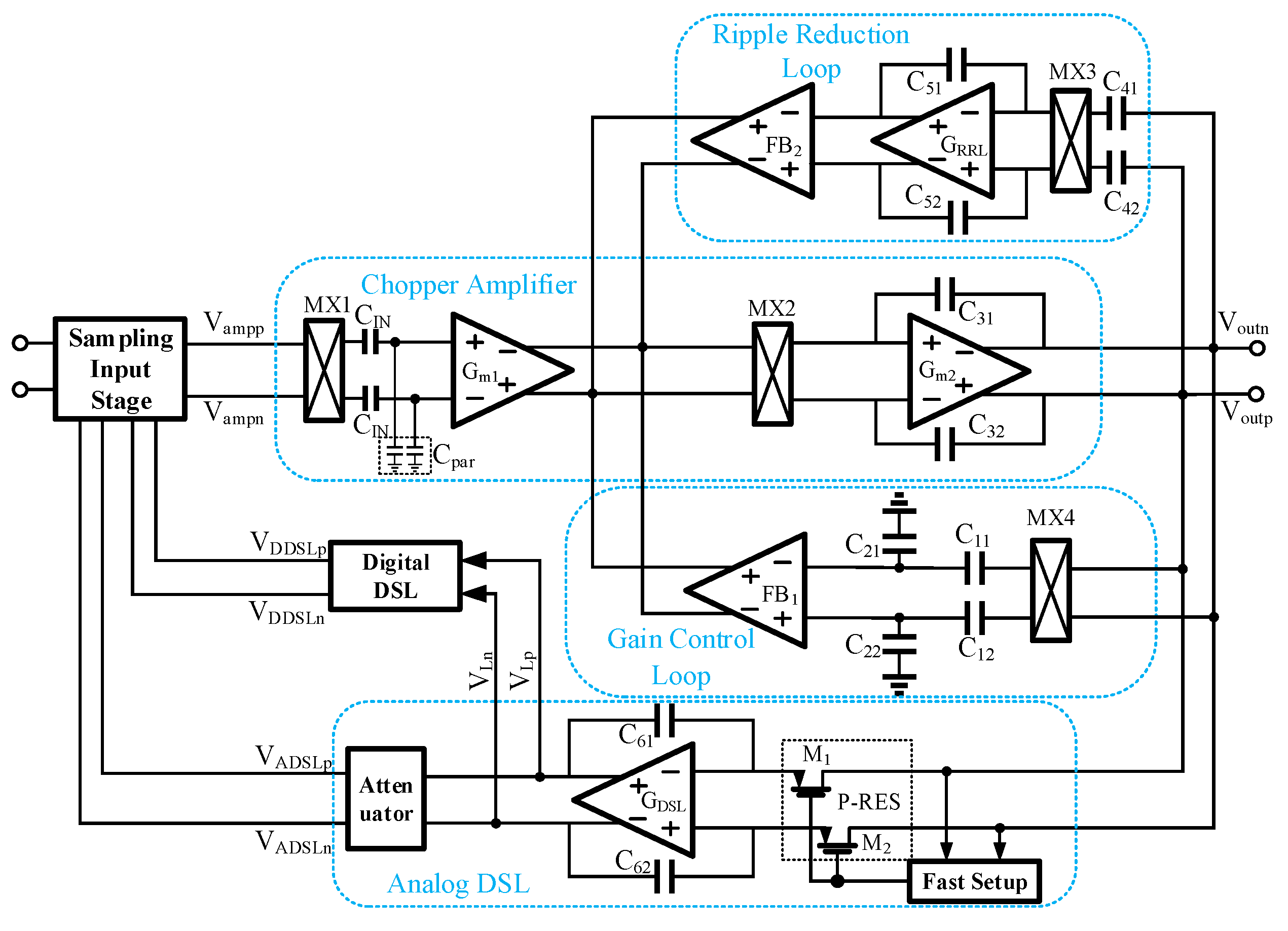
2. System Overview
3. Circuit Implementation
3.1. Two-Stage Chopper Amplifier
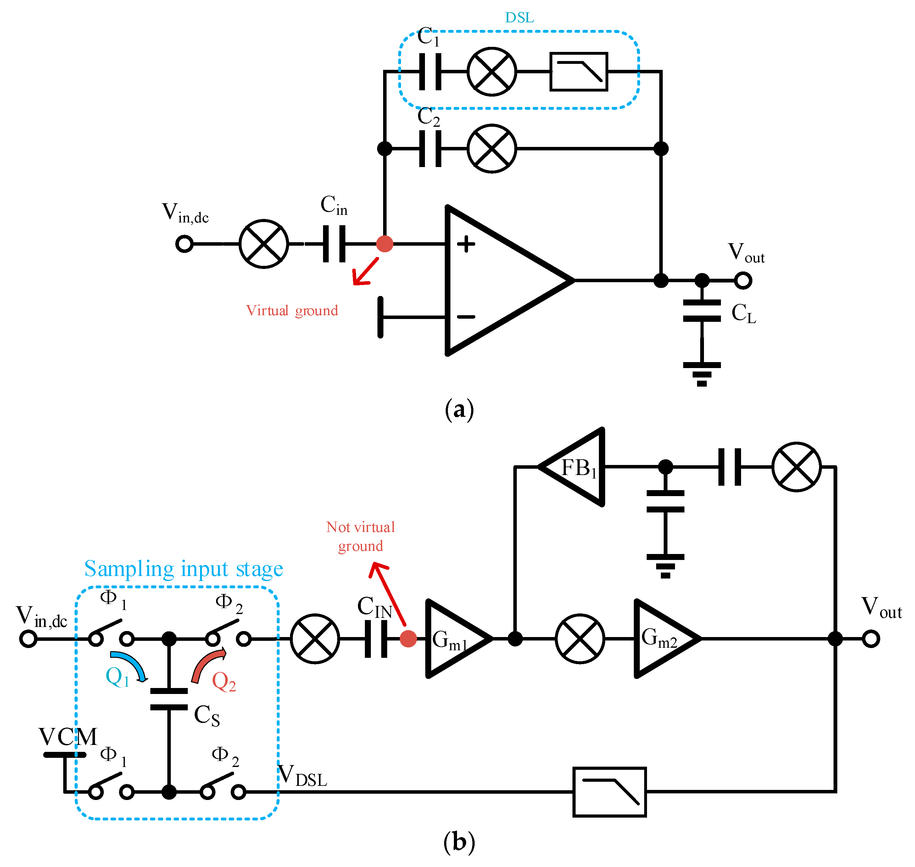
3.2. Sampling Input Stage and Input Impedance
3.2.1. Sampling Input Stage
3.2.2. Input Impedance
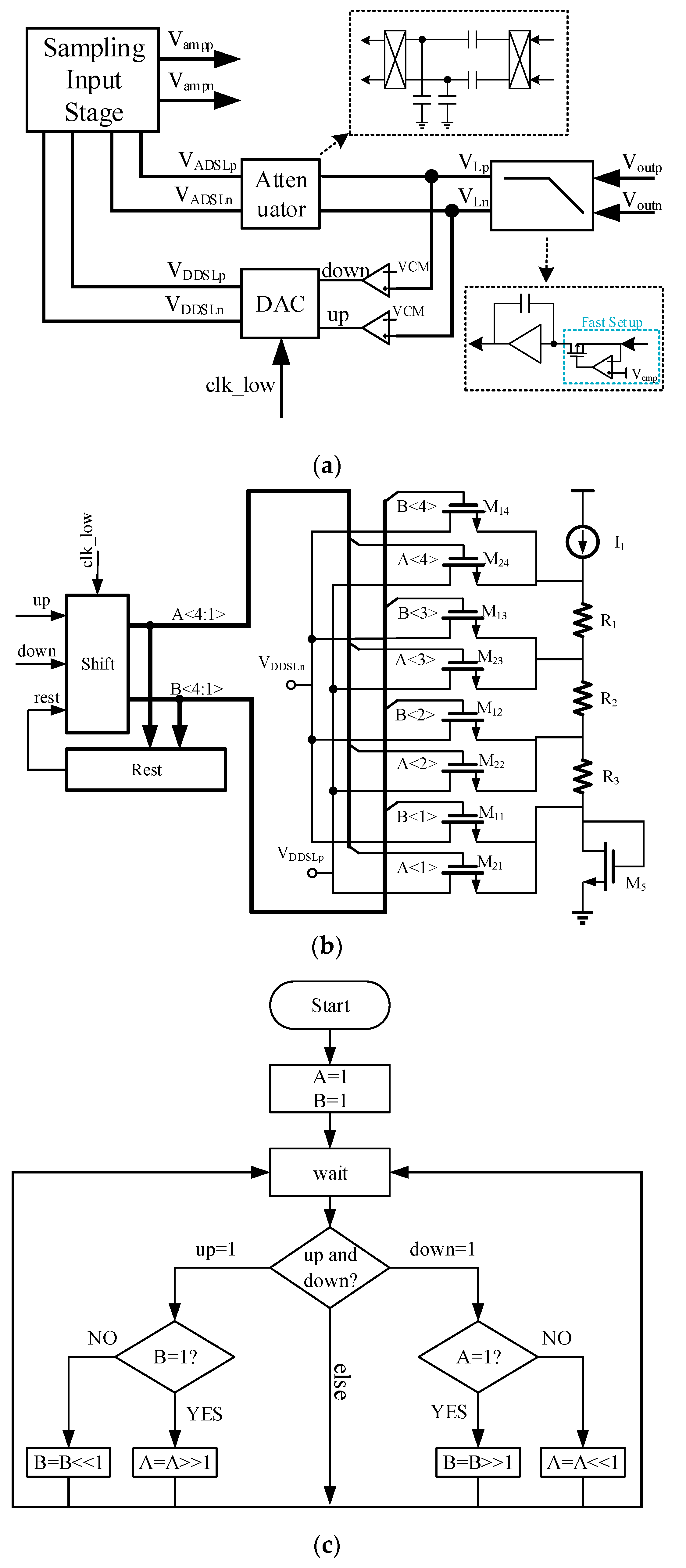
3.3. Digital-Analog Hybrid DC-Servo Loop
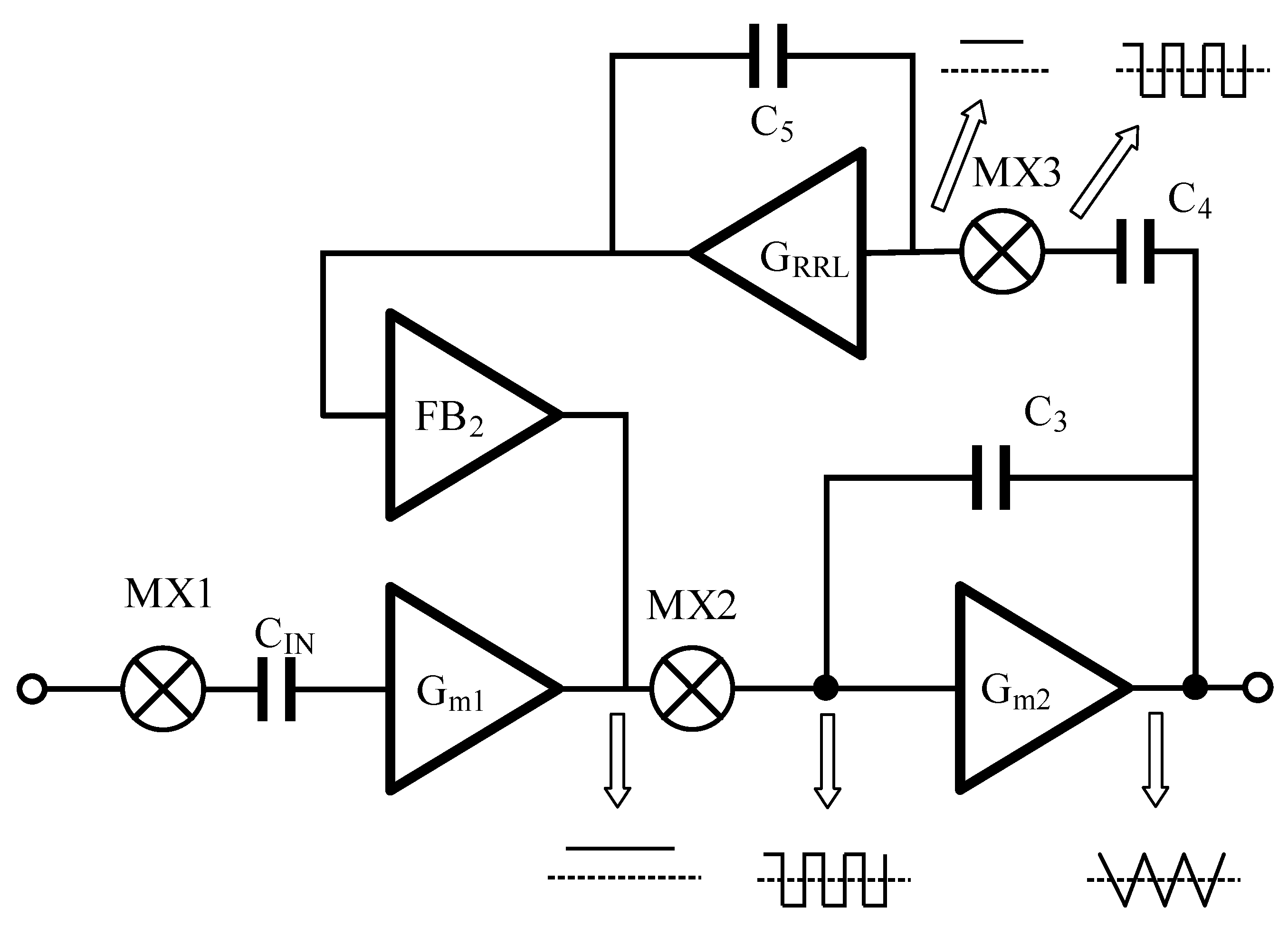
3.4. Ripple Reduction Loop (RRL)
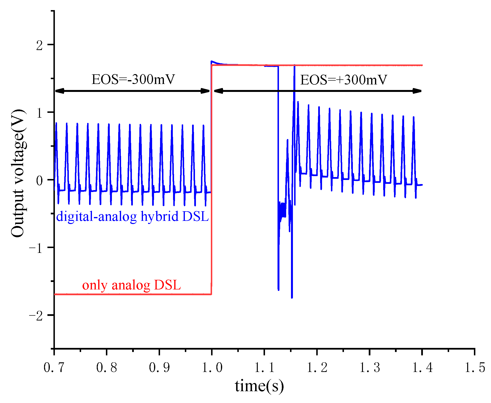
4. Simulated Results
5. Conclusions
Author Contributions
Funding
Conflicts of Interest
References
- World Health Organization. Available online: https://www.who.int/health-topics/cardiovascular-diseases/ (accessed on 17 May 2017).
- Honka, A.; Kaipainen, K.; Hietala, H.; Saranummi, N. Rethinking Health: ICT-Enabled Services to Empower People to Manage Their Health. IEEE Rev. Biomed. Eng. 2011, 4, 119–139. [Google Scholar] [CrossRef] [PubMed]
- Chi, Y.M.; Jung, T.; Cauwenberghs, G. Dry-Contact and Noncontact Biopotential Electrodes: Methodological Review. IEEE Rev. Biomed. Eng. 2010, 3, 106–119. [Google Scholar] [CrossRef] [PubMed]
- Xu, J.; Mitra, S.; Hoof, C.V.; Yazicioglu, R.F.; Makinwa, K.A.A. Active Electrodes for Wearable EEG Acquisition: Review and Electronics Design Methodology. IEEE Rev. Biomed. Eng. 2017, 10, 187–198. [Google Scholar] [CrossRef] [PubMed]
- Xu, J.; Mitra, S.; Matsumoto, A.; Patki, S.; Hoof, C.V.; Makinwa, K.A.A.; Yazicioglu, R.F. A Wearable 8-Channel Active-Electrode EEG/ETI Acquisition System for Body Area Networks. IEEE J. Solid-State Circuits 2014, 49, 2005–2016. [Google Scholar] [CrossRef]
- Denison, T.; Consoer, K.; Santa, W.; Avestruz, A.; Cooley, J.; Kelly, A. A 2 μW 100 nV/√Hz Chopper-Stabilized Instrumentation Amplifier for Chronic Measurement of Neural Field Potentials. IEEE J. Solid-State Circuits 2007, 42, 2934–2945. [Google Scholar] [CrossRef]
- Fan, Q.; Sebastiano, F.; Huijsing, J.H.; Makinwa, K.A.A. A 1.8 μW 60 nV/√Hz Capacitively-Coupled Chopper Instrumentation Amplifier in 65 nm CMOS for Wireless Sensor Nodes. IEEE J. Solid-State Circuits 2011, 46, 1534–1543. [Google Scholar] [CrossRef]
- Chandrakumar, H.; Marković, D. A High Dynamic-Range Neural Recording Chopper Amplifier for Simultaneous Neural Recording and Stimulation. IEEE J. Solid-State Circuits 2017, 52, 645–656. [Google Scholar] [CrossRef]
- Wu, J.; Law, M.; Mak, P.; Martins, R.P. A 2-μW 45-nV/√Hz Readout Front End with Multiple-Chopping Active-High-Pass Ripple Reduction Loop and Pseudofeedback DC Servo Loop. IEEE Trans. Circuits Syst. II Express Briefs 2016, 63, 351–355. [Google Scholar] [CrossRef]
- Yazicioglu, R.F.; Merken, P.; Puers, R.; Hoof, C.V. A 200 μW Eight-Channel EEG Acquisition ASIC for Ambulatory EEG Systems. IEEE J. Solid-State Circuits 2008, 43, 3025–3038. [Google Scholar] [CrossRef]
- Wu, C.-M.; Chen, H.-C.; Yen, M.-Y.; Yang, S.-C. Chopper-Stabilized Instrumentation Amplifier with Automatic Frequency Tuning Loop. Micromachines 2018, 9, 289. [Google Scholar] [CrossRef] [PubMed]
- Zheng, J.; Ki, W.; Hu, L.; Tsui, C. Chopper Capacitively Coupled Instrumentation Amplifier Capable of Handling Large Electrode Offset for Biopotential Recordings. IEEE Trans. Circuits Syst. II Express Briefs 2017, 64, 1392–1396. [Google Scholar] [CrossRef]
- Rong, W.; Makinwa, K.A.A.; Huijsing, J.H. A chopper current-feedback instrumentation amplifier with a 1 mHz 1/f noise corner and an AC-coupled ripple-reduction loop. IEEE Int. Solid-State Circuits 2009, 44, 322–323. [Google Scholar]
- Chen, M.; Chun, H.S.; Castro, I.D.; Torfs, T.; Lin, Q.; Hoof, C.; Wang, G.; Lian, Y.; Helleputte, N. A 400 GΩ Input-Impedance Active Electrode for Non-Contact Capacitively Coupled ECG Acquisition with Large Linear-Input-Range and High CM-Interference-Tolerance. IEEE Trans. Biomed. Circuits Syst. 2019, 13, 376–386. [Google Scholar] [CrossRef] [PubMed]
- Khatavkar, P.; Aniruddhan, S. 432 nW per Channel 130 nV/√Hz ECG Acquisition Front End with Multifrequency Chopping. IEEE Trans. Large Scale Integr. (VLSI) Syst. 2019, 27, 2021–2032. [Google Scholar] [CrossRef]
- Li, Q.; Wang, X.; Liu, Y. A 60 nV√Hz <0.01%-THD ±200 mV-DC-Rejection Bio-sensing Chopper Amplifier with Noise-Nonlinearity-Cancelling Loop. IEEE Trans. Circuits Syst. II Express Briefs. in press. [CrossRef]


| Parameter | [12] JSSC’17 | [8] JSSC’17 | [14] TBCAS’19 | [15] VLSI’19 | [16] TCSII’19 | This Work |
|---|---|---|---|---|---|---|
| Technology | 130 nm | 40 nm | 180 nm | 130 nm | 180 nm | 180 nm |
| Supply (V) | 1.2 | 1.2 | 5 | 1.2 | 1.2 | 1.8 |
| Bandwidth (Hz) | 0.6–8 k | 1–200 | 0.5–100 | 0.2–100 | 0.5–500 | 0.6–1k |
| Low-frequency cut-off (Hz) | 0.6 | 10 | 0.5 | 0.2 | 0.5 | 0.6 |
| Input Impedance (Ω) | - | 20 M | 5 G | 10 M | 1 G | 2.1 G |
| dc Input Impedance (Ω) | 2.5 M | 300 M | 400 G | 200 M | - | 120 G |
| EOS range (mV) | ±50 | ±50 | - | - | ±200 | ±325 |
| Input-referred Noise (μVrms) | 1 | 2 | 3.7 | 1.31 | 1.8 | 1.9 |
| GAIN (dB) | 40 | 26 | 0/9/13/20 | 40 | 40 | 46 |
| Supply current (μA) | 2.9 | 1.7 | 18 | 0.36/ch | 2 | 11 |
| CMRR (dB) | 85 | - | 70 | 98 | 90 | 96 |
| AREA (mm2) | 0.3 | 0.071/ch | 1.23 | 0.68 | 0.46 | 0.36 |
| Application | ECG | Neural | ECG | ECG | ECG | ECG |
© 2020 by the authors. Licensee MDPI, Basel, Switzerland. This article is an open access article distributed under the terms and conditions of the Creative Commons Attribution (CC BY) license (http://creativecommons.org/licenses/by/4.0/).
Share and Cite
Xu, W.; Wang, T.; Wei, X.; Yue, H.; Wei, B.; Duan, J.; Li, H. Low Noise, High Input Impedance Digital-Analog Hybrid Offset Suppression Amplifier for Wearable Dry Electrode ECG Monitoring. Electronics 2020, 9, 165. https://doi.org/10.3390/electronics9010165
Xu W, Wang T, Wei X, Yue H, Wei B, Duan J, Li H. Low Noise, High Input Impedance Digital-Analog Hybrid Offset Suppression Amplifier for Wearable Dry Electrode ECG Monitoring. Electronics. 2020; 9(1):165. https://doi.org/10.3390/electronics9010165
Chicago/Turabian StyleXu, Weilin, Taotao Wang, Xueming Wei, Hongwei Yue, Baolin Wei, Jihai Duan, and Haiou Li. 2020. "Low Noise, High Input Impedance Digital-Analog Hybrid Offset Suppression Amplifier for Wearable Dry Electrode ECG Monitoring" Electronics 9, no. 1: 165. https://doi.org/10.3390/electronics9010165
APA StyleXu, W., Wang, T., Wei, X., Yue, H., Wei, B., Duan, J., & Li, H. (2020). Low Noise, High Input Impedance Digital-Analog Hybrid Offset Suppression Amplifier for Wearable Dry Electrode ECG Monitoring. Electronics, 9(1), 165. https://doi.org/10.3390/electronics9010165