1. Introduction
The monitoring of defects occurring through the operation of highly loaded structures is important for the economy and for people’s safety. The sheathing of aircraft, sea vessels, bridge supports, structural elements of construction equipment, drilling rigs, etc., undergo periodic and static loading during operation. As a result, fatigue cracks appear in the material of these structures. This can lead to the destruction of the structure [
1,
2,
3].
Over the past decade, a number of new methods and devices for nondestructive testing have been developed. These aids are characterized by ease of automation, autonomy, and the ability to monitor while the monitored object is in its operation mode [
4,
5,
6,
7,
8,
9,
10].
This work is focused on the development of a method for detecting surface defects such as cracks, and a defect monitoring system that makes it possible to realize this method. In [
11], we proposed to use the fact that, under the influence of external loads, surface cracks are opened and, if a thin film is deposited onto the surface, this film will also undergo stresses, and therefore can be torn. Only the case when stresses normal to the crack walls are applied to a surface-cracked object is studied. This case is also known as a tensile or opening mode. Such impacts can lead to further rapid growth of the crack, since the vertices of the crack in this case raise the stress, and the material in these areas is therefore subjected to increased loads. Situations when the object undergoes torsional or bending deformations were not considered.
The authors developed a model of a layered structure in which a thin metal film was deposited on a dielectric polymer material located above a surface crack [
11]. This model indicated that tensile stresses create a high level of stress in a thin metal film over a crack (as a result of modeling an aluminum plate with a 50 μm depth crack and coated with 50 μm thick polyimide film and 30 μm thick copper film, 12–13.5 GPa stress appeared in the copper film material above the crack) and can lead to its rupture. In the reference data, the authors did not find values for the tensile strength of copper exceeding 450 MPa.
Nowadays, the pool of materials that are easily applied to the surface of the object, have good adhesion to it, and the conductivity of which can be varied within wide limits, is sufficiently large. A good choice in this case may be polymer films, which can be doped to obtain conductivity values of the order of 10
3 S/cm or higher [
12], or to incorporate carbon nanotubes in their composition that provide new useful properties [
13,
14,
15]. The use of polymers makes it possible to fabricate both a dielectric and conductive layer of a single material, which can be useful. The problems of adhesion and possible peeling of films have not been specifically studied. The authors suggest that, since similar fastening methods are used, for example, in strain gauges, the problem of ensuring good adhesion can be solved by developing a system manufacturing technology.
The construction of a distributed crack sensor and the method of its registration based on the above considerations have been proposed in [
16]. In this paper, the proposed construction is significantly improved. Using a combination of multiplexers and semiconductor switches allowed the inclusion not only of the conducting lines of the distributed crack sensor, but also the segments of those lines in the measuring circuit, in the required order.
The purpose of this work is to develop a monitoring system for surface defects, the algorithm of the system and its structural scheme, the functional scheme and design of the distributed crack sensor, and a model in the form of VHDL (VHSIC (Very high speed integrated circuits) Hardware Description Language)-description.
2. System of Surface Defect Monitoring
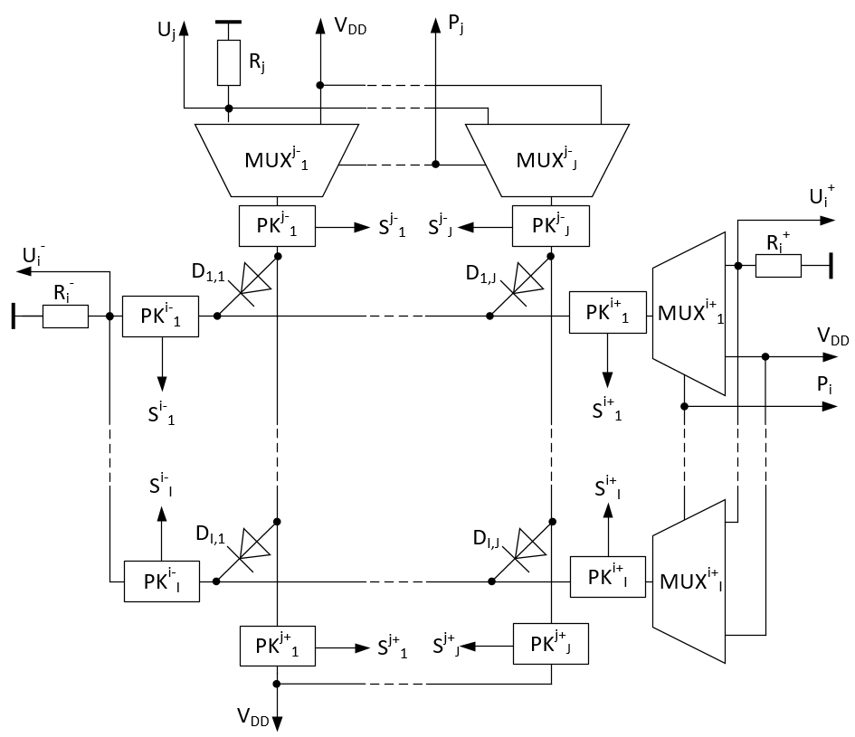
The functional scheme and the design of the distributed crack sensor are shown in
Figure 1.
The distributed crack sensor consists of two layers of thin-film conductors arranged orthogonally (
Figure 1b). The number of conductors of the first layer is
I, the second is
J. Conductors are isolated from each other and, if necessary, from the surface of the controlled object by dielectric films (
Figure 1b). The electrical connection between the conductors is carried out by means of diodes D
i,j, which are located at the intersections of the conductors of the first and second layers. The section of a conductor between two nearby diodes will be referred to as a segment. Indices of a segment are determined by the numbers of the corresponding lines. To check the integrity of the lines using multiplexers MUX and passkeys PK, the lines are alternately connected (and, for broken lines, connecting their segments one by one) to the V
DD power supply and the load resistor (
Figure 1a).
The integrity of the conductors is monitored by voltage levels at the outputs Ui−, Ui+ and Uj. Low voltage levels at these outputs indicate a break in the line or segment, and high levels indicate its integrity.
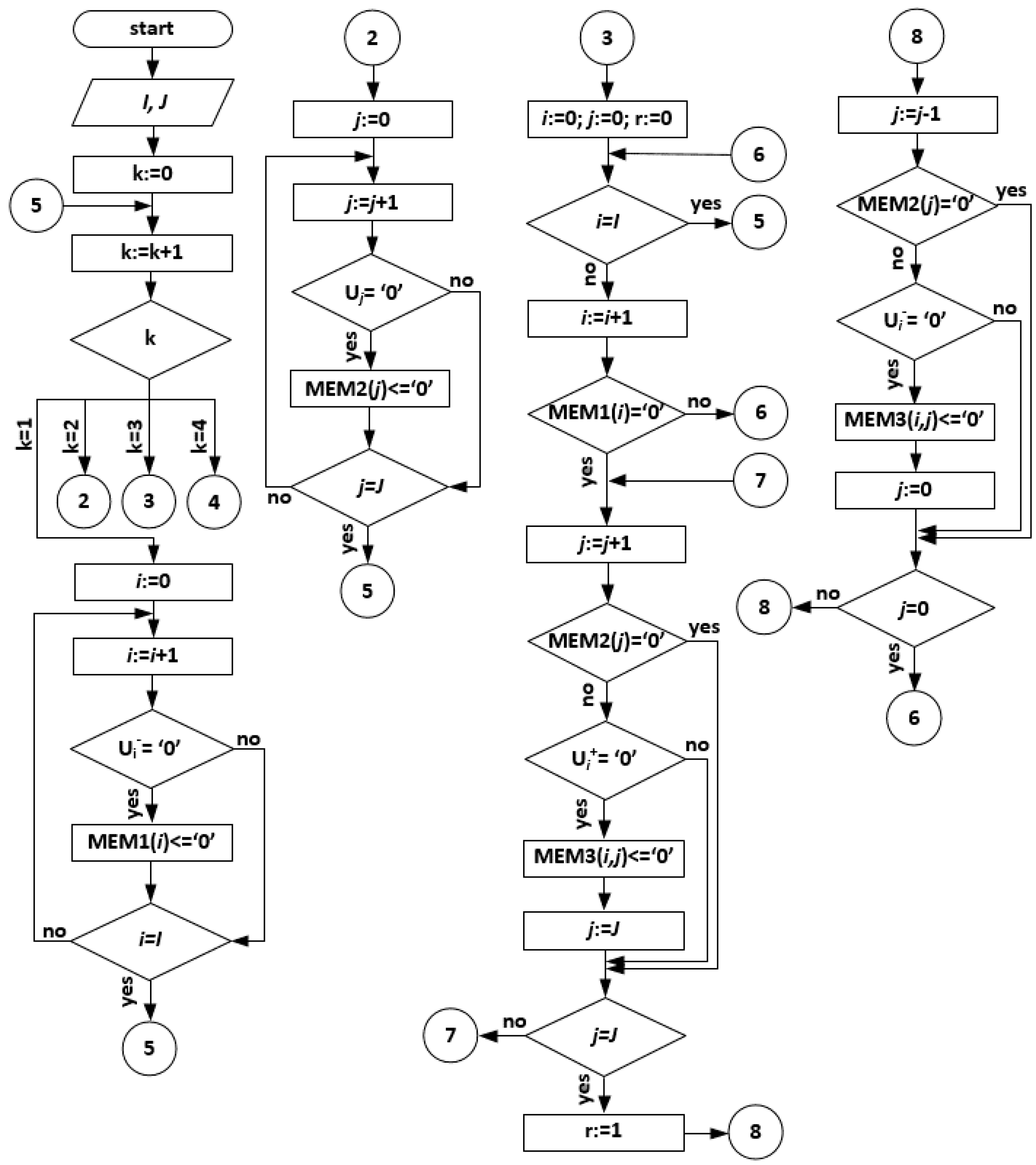
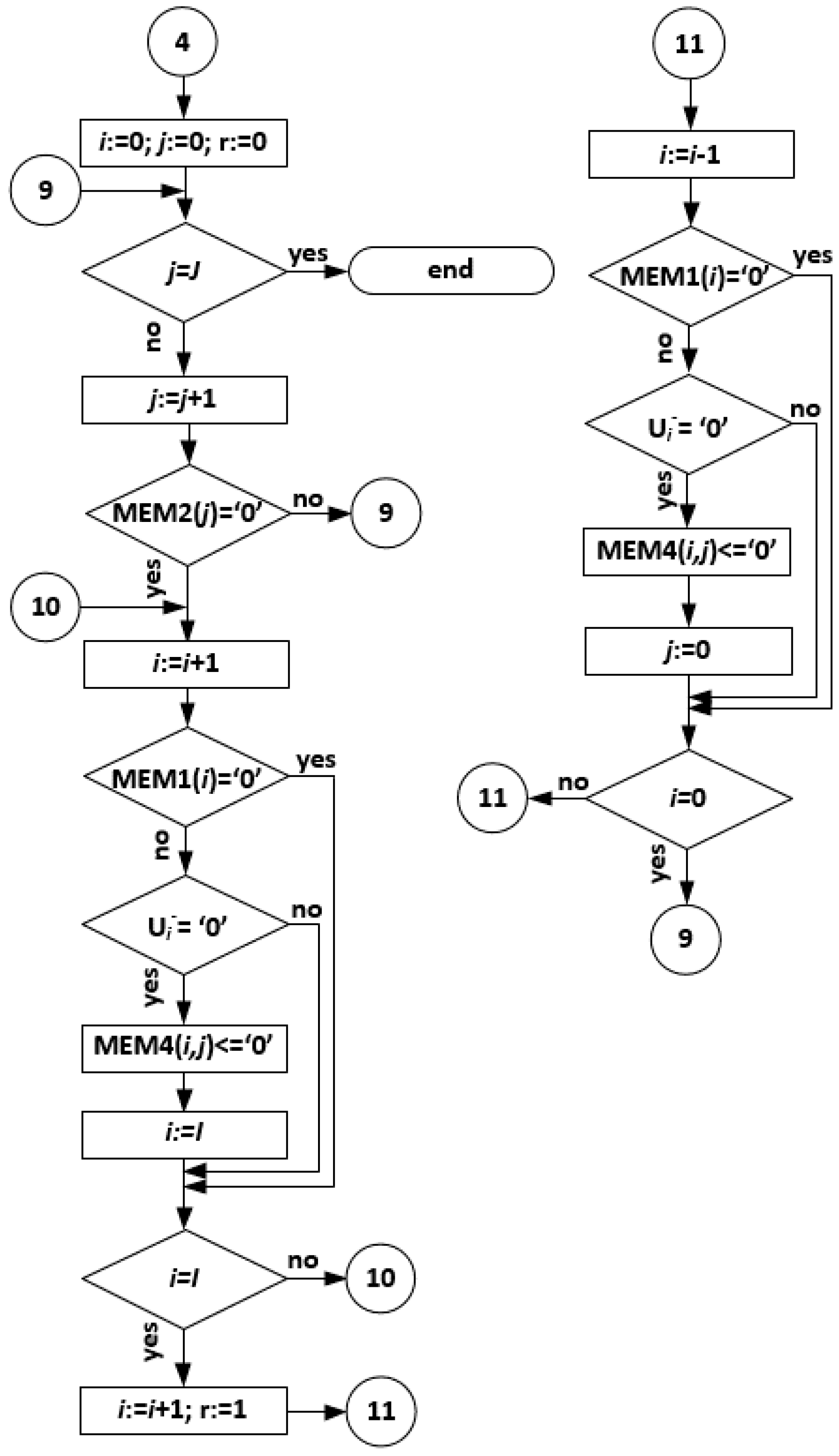
We developed the algorithm for the operation of the surface defect monitoring system. Its block diagram is shown in
Figure 2 and
Figure 3.
A full cycle of checking conductors for integrity is implemented using four system modes (k—mode number). In the first mode, the integrity of the conductors of the first layer with indices i = 1, 2, ..., I is checking. Multiplexers from MUXi+1 to MUXi+I connect all i-th lines to the supply voltage VDD in parallel using the control signal Pi, and the keys from PKi−1 to PKi−I and from PKi+1 to PKi+I alternately include each i-th line in the circuit. If the line is damaged, a low voltage level is registered on the Ui− pin and a logical ‘0’ is written to the memory cell corresponding to the number of the damaged line in random access memory (RAM) MEM1 with one-dimensional addressing. Accordingly, the number of cells in memory MEM1 is equal to the number of lines I.
In the second mode, the lines with indices j = 1, 2, ..., J are similarly checked. At a low voltage level at the output Uj, ‘0’ is written to the memory cell corresponding to the number of the line currently being checked in the RAM MEM2 with one-dimensional addressing. The number of cells in memory MEM2 is equal to the number of j-th lines.
In the third and fourth modes, all segments of defective i-th and j-th lines are checked, respectively. This is done to clarify the location of the defect.
In the third mode, the voltage VDD is applied to the first defective i-th line in order of increasing number through the multiplexer MUXi+i and the key PKj+i corresponding to the first right defect-free j-th line, and the voltage at the terminal Ui+ is checked. If the signal passes (high voltage level on Ui+), this segment is considered to be defect-free, and the power voltage VDD is connected to the previous defect-free j-th line through the key PKj+i. If a low voltage level at the Ui+ pin is registered, the segment under investigation is considered damaged. In this case, ‘0’ is written to the memory MEM3 with two-dimensional addressing at the address corresponding to the segment index. Further, the segments belonging to this i-th line are checked in reverse order by including the key PKi−i corresponding to the defective i-th line and the key PKj+j corresponding to the first left defect-free j-th line, and then the sorting of j-th lines is carried out in order of increasing number. The damage of the segment is checked based on the presence of a low voltage level at the output Ui−.
After checking all defective i-lines, the segments of defective j-lines are checked in the fourth mode in the same way, and the verification cycle is completed.
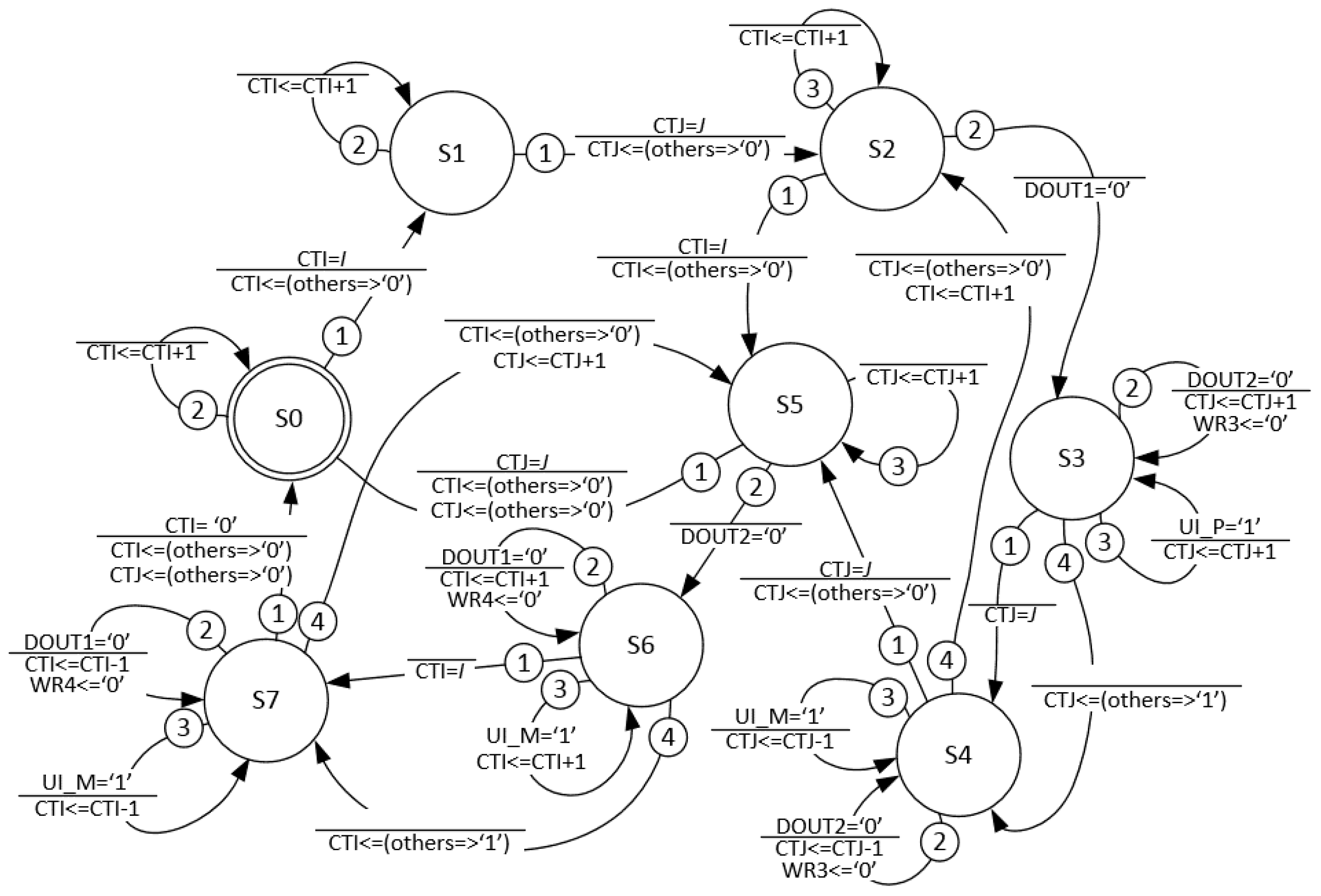
This operation algorithm is implemented as a finite-state machine, the graph of which is shown in
Figure 4.
The states of the finite-state machine are given in
Table 1. The finite-state machine can be in one of the eight states S0–S7.
Signal designations in
Table 1 correspond to
Figure 4. Signals WR1 and WR2, taking the value ‘1’, allow the writing of a bit to the cells of memory MEM1 and MEM2, respectively. Signals WR3 and WR4, taking the value ‘1’, allow the writing of a bit to the cells of RAM MEM3 and MEM4, which stores information about defective segments of the
i-th and
j-th lines. The DIN3 signal determines the connection of the MEM3 and MEM4 data input lines to the U
i+ or U
i− lines, in accordance with the current checking order of the segments of the defective
i-th line. Signals SI_M, SI_P, SJ_M and SJ_P control semiconductor switches PK in accordance with the current operating mode of the system. The signal P
i controls multiplexers MUX
i+I and determines the connection of the
i-th lines to the power supply V
DD or to the load resistor R
i+. The signal P
j controls the multiplexers MUX
j+j and determines the connection of
j-th lines to the supply V
DD or to the load resistor R
j.
The states S0 and S1 of the finite-state machine correspond to the first and second mode k of the system operation algorithm shown in
Figure 2 and
Figure 3. In the state S2, the RAM MEM1 is checked, and if there are cells in the memory MEM1 where the value ‘0’ is stored, the first (in order of increasing number)
i-th line is selected, at the address of which the value ‘0’ is stored in the memory cell. If there are no zeros in MEM1, the finite-state machine goes to state S5. In the state S3, all segments of the defective
i-th line are examined from right to left; in state S4, from left to right. In the state S5, as in S2, the RAM MEM2 is checked, and if there are cells where the value ‘0’ is stored, the first (in order of increasing number)
j-th line is selected, at the address of which the value ‘0’ is stored in the memory cell. If there are no damaged lines among the
j-lines, the transition to the initial state S0 is carried out. In the state S6, all segments of the
j-th damaged line are checked from the bottom up; in the state S7, from the top down (this orientation corresponds to
Figure 1a). After checking all the segments of the damaged
j-lines, the transition to the initial state S0 follows.
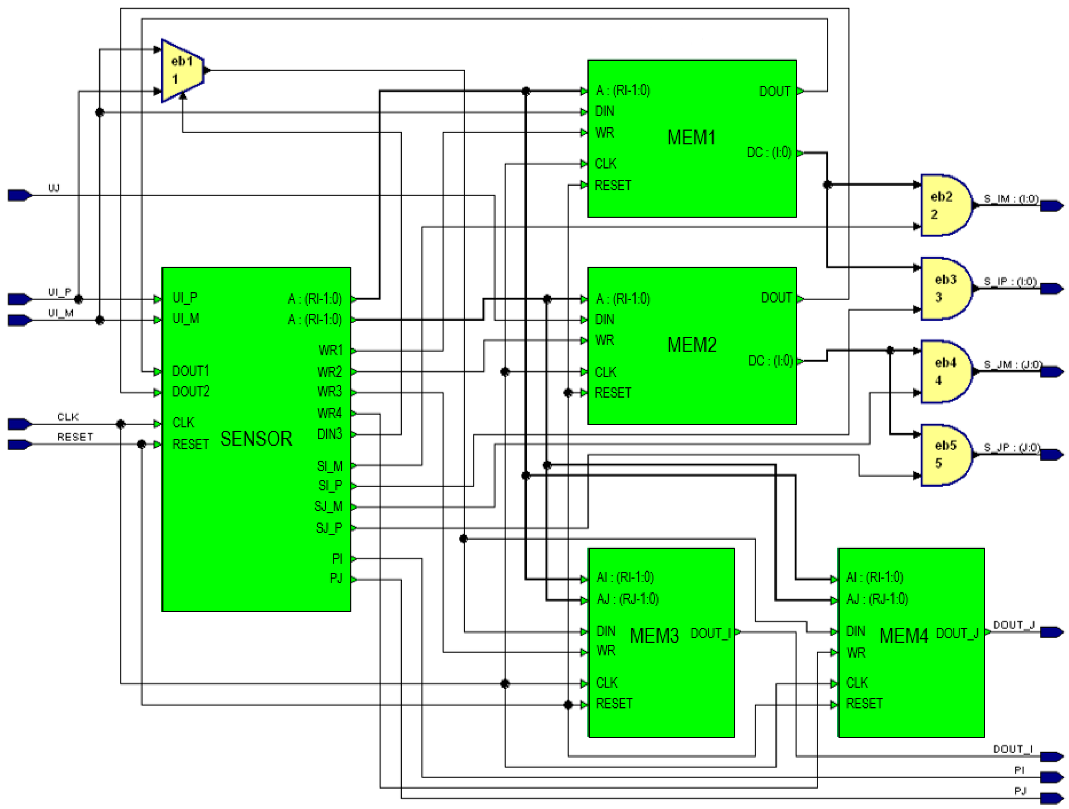
The developed structural scheme of the surface defect monitoring system is shown in
Figure 5.
The system consists of a control block SENSOR and memory blocks MEM1, MEM2, MEM3 and MEM4. The control block is a clocked finite-state machine, the graph of which is shown in
Figure 4. Memory blocks MEM1 and MEM2—with one-dimensional addressing—consist of single-digit cells, the number of which is
I and
J, respectively. Memory blocks MEM3 and MEM4—with two-dimensional addressing—consist of single-digit cells, the number of which is
I ×
J. Two memory blocks are used for each memory block MEM3 and MEM4, since the total number of segments is 2(
I ×
J). At the time the system is turned on, the RESET signal, assuming a value of ‘1’, initiates the recording of logical ‘1’ into all the cells of the memory blocks MEM1, MEM2, MEM3 and MEM4.
Thus, by the end of the finite-state machine cycle, the results of checking the integrity of the segments of thin-film conducting lines are in the memory blocks MEM3 and MEM4. Then, the information from the outputs DOUT_I and DOUT_J goes to the computer for further processing.


