1. Introduction
Background and concept. The memristor (abbreviated from memory + resistor) is the fourth electrical passive two-terminal element alongside with the resistor, inductor, and capacitor [
1,
2]. The memristor is a nonlinear electrical element [
1]. It directly relates the electric charge
q and the magnetic flux linkage
Ψ [
1,
2]. Leon Chua forecast the memristor element in 1971 in accordance to symmetry considerations and the relationships between the four basic electrical quantities—voltage, current, charge, and magnetic flux [
1]. The memristor element has the property for memorizing the amount of charge passed through its intersection (in given limits depending on the geometrical dimensions of the element) and its respective resistance (conductance), which is proportional to the electric charge accumulated in the memristor when the electric sources are switched off [
2]. The Weber-Coulomb relationship of the memristor is a nonlinear single-valued curve, while its respective current-voltage relationship is a pinched-hysteresis loop, which shape and area depend on the amplitude and on the frequency of the applied voltage [
2]. Due to the effect of memorizing the resistance of the memristor after switching off the electrical sources, it could be used as a non-volatile memory element [
2]. Its physical prototype made by titanium dioxide [
2,
3,
4] has physical dimensions in the nano scale range and its power consumption is several times lower than the existing flash memories [
2]. These facts are good preconditions for the future applications of the memristor matrices in computer memories [
2]. The memristor element is a good candidate for application in the neuromorphic engineering, in the synapses in the artificial neural networks, in the analog and digital electronics as well [
2].
The first physical prototype of the memristor element predicted by L. Chua in 1971 [
1] was invented in the HP research labs by Stanley Williams research team in 2008 [
2]. After this flash, many scientific papers associated with memristors and memristive devices have been published and several basic memristor models have been proposed [
2,
3,
4,
5,
6,
7,
8,
9,
10]. Each of the basic memristor models—the linear drift model proposed by Strukov and Williams [
2] and the nonlinear drift models made by Joglekar [
3], Pickett [
4,
5], and Biolek [
6]—is appropriate for specific electrical modes for the operation of the memristor elements. The linear ionic drift model [
2] is used for low memristor voltages and the nonlinear drift models of Biolek and Joglekar are able to represent the memristor nonlinear drift behavior for high voltages when the memristor element has highly nonlinear performance [
3,
6]. The Pickett memristor model [
4,
5] is based on laboratory experiments and measurements, and on the current flow through a tunnel barrier. It has the highest accuracy and sometimes it is used as a reference model [
4,
5], but it is very complicated and it is not always appropriate for computer simulations due to convergence problems. The Boundary Condition Memristor (BCM) Model is with linear dopant drift and switch-based window function for representation the boundary effects [
7]. It is able to represent both the soft-switching and hard-switching memristor modes [
7]. The Generalized BCM model (GBCM) created by Ascoli, Corinto, and Tetzlaff, is almost identical with the BCM model but the difference is the use of activation threshold not only for the boundaries but also for every value of the state variable [
8]. The lack of a realistic versatile memristor model suitable for simulations, having a nonlinear dopant drift and accuracy near to the Pickett model was the motivation of the present research. The new model proposed in this paper is based both on Biolek and on the GBCM models but it uses a combination of a Biolek window function and an additional weighted sinusoidal window function for increasing the nonlinearity of the ionic drift. The new ideas of the memristor model proposed here are that the weight coefficient in front of the additional sinusoidal window function component and the respective extent of nonlinearity of the memristor dopant drift could be changed and adjusted till the basic relationship of the memristor are almost near to these obtained by the Pickett model for the same conditions. If the activation threshold and the coefficient in front of the weighted sinusoidal window function are equal to zero the original Biolek model is obtained. The Biolek memristor model is a special case of the modified Biolek model. The boundary effects observable for hard-switching mode are represented using the switch-based algorithm of the GBCM model. After comparison with the Pickett memristor model the modified Biolek model was adjusted so its current-voltage and the Weber-Coulomb relationships were obtained similar to the Pickett reference model. The precision of the modified Biolek model is near to the accuracy of the Pickett memristor model but the computer tests confirmed that the modified Biolek model does not have convergence problems and it is appropriate for computer simulations of memristors and memristive circuits.
In
Section 2, the description of the titanium-dioxide memristor element according to the Pickett Tunnel Barrier model is presented and the main relationships are obtained. The basic ideas and the major relationships of the modified Biolek model are shown in
Section 3. The pseudo-code based algorithm of the modified Biolek model for computer simulations is presented in
Section 4. The comparison with the Pickett memristor model, the adjusting process of the modified Biolek model, and the basic results are presented and discussed in
Section 5. A comparison of the model proposed here with Joglekar memristor model is presented and discussed in
Section 6. The concluding remarks are presented in
Section 7.
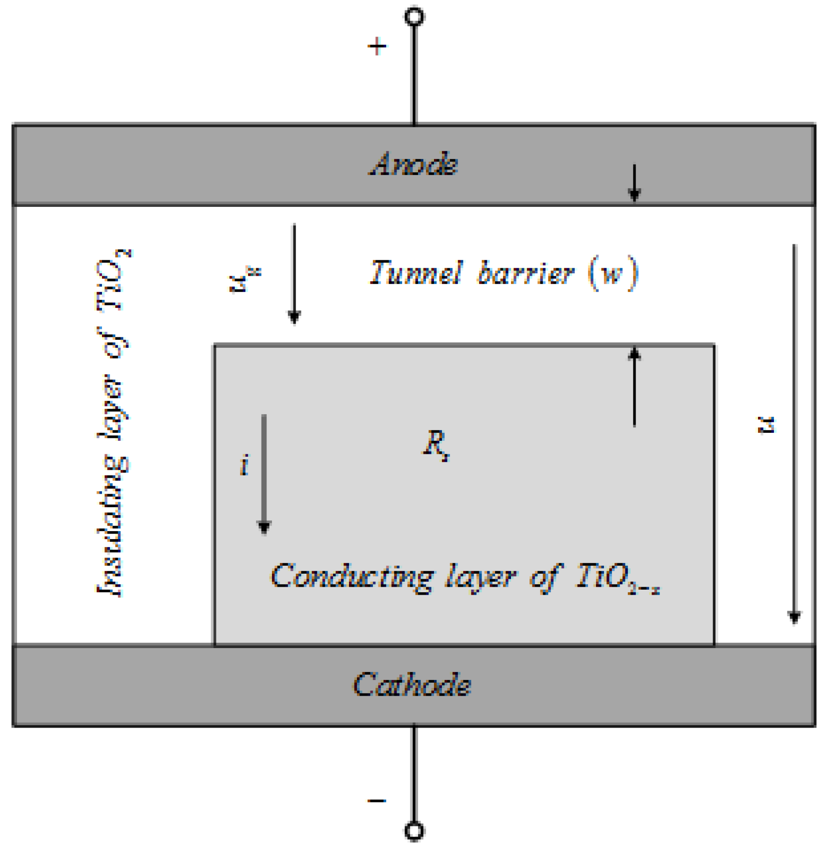
2. A Brief Description of the Memristor According to the Pickett Tunnel Barrier Model
The structure of a memristor cell according to the Pickett’s model [
5] is shown in
Figure 1. The electrodes are made of platinum and the insulating layer is made of pure titanium dioxide. The conducting channel in the memristor cell is formed by a thin layer of doped with oxygen vacancies titanium dioxide material. There is also a thin tunnel barrier with a length of
w. The resistance of the conducting layer is approximately equal to
Rs = 215 Ω [
4,
5].
When the memristor is switched in open state (
i > 0), the differential equation has to be expressed with (1) [
5]. Formulas (2)–(11) are also according to [
5].
The parameters used in (1) and their corresponding values [
5] are given in
Table 1.
When the memristor is switched in closed state (
i < 0) [
5], the differential equation is:
The parameters and their values [
5] are given in
Table 2.
The current flowing through the tunnel barrier of the memristor element [
5] is:
where
ug is the voltage drop over the tunnel barrier [
5]. This voltage drop could be expressed using the Kirchhoff’s Voltage Law (KVL) and the voltage
u over the memristor element [
5,
11]:
The constant
j0 [
5] could be expressed as follows:
where
e is the elementary charge of the electron,
h is the Planck’s constant.
The area of the tunnel junction [
5] is equal to
A = 10
4 nm
2.
The deviation of the length of the tunnel junction [
5] is:
The second term of (6) [
5] is:
where Φ
0 = 0.95 V is the height of the potential barrier. The quantity λ [
5] from Equation (7) is expressed as follows:
where
k = 5 is the permittivity of the titanium dioxide material,
ε0 = 8.85∙10
−12 F/m [
5] is the absolute permittivity of the vacuum space.
After transformation of (7) it is obtained that w
1 = 0.126 nm. Using (6) and according to [
5] the following Equation (9) is derived:
The quantity
B [
5] is expressed as follows:
where
m is the electron weight. The quantity Φ
1 [
5] is:
The Pickett memristor model [
5] is fully described with Equations (1)–(11). A Simulation Program with Integrated Circuit Emphasis (SPICE) code of Pickett model [
5] is created using (1)–(11) and it is used for simulation of the memristor element.
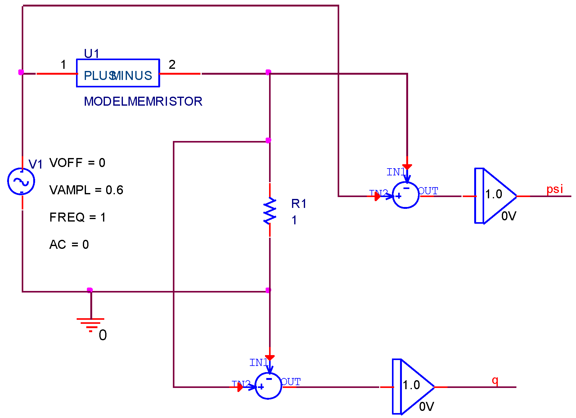
The memristor circuit under test is presented in
Figure 2. It is created of a sinusoidal voltage source, a series resistor with very small resistance (
R1 = 1 Ω), a difference devices, and integrators. The magnetic flux linkage is obtained as a time integral of the voltage drop across the memristor, and the electric charge is the time integral of the memristor current and, respectively, the voltage drop across the resistor
R1 [
11].
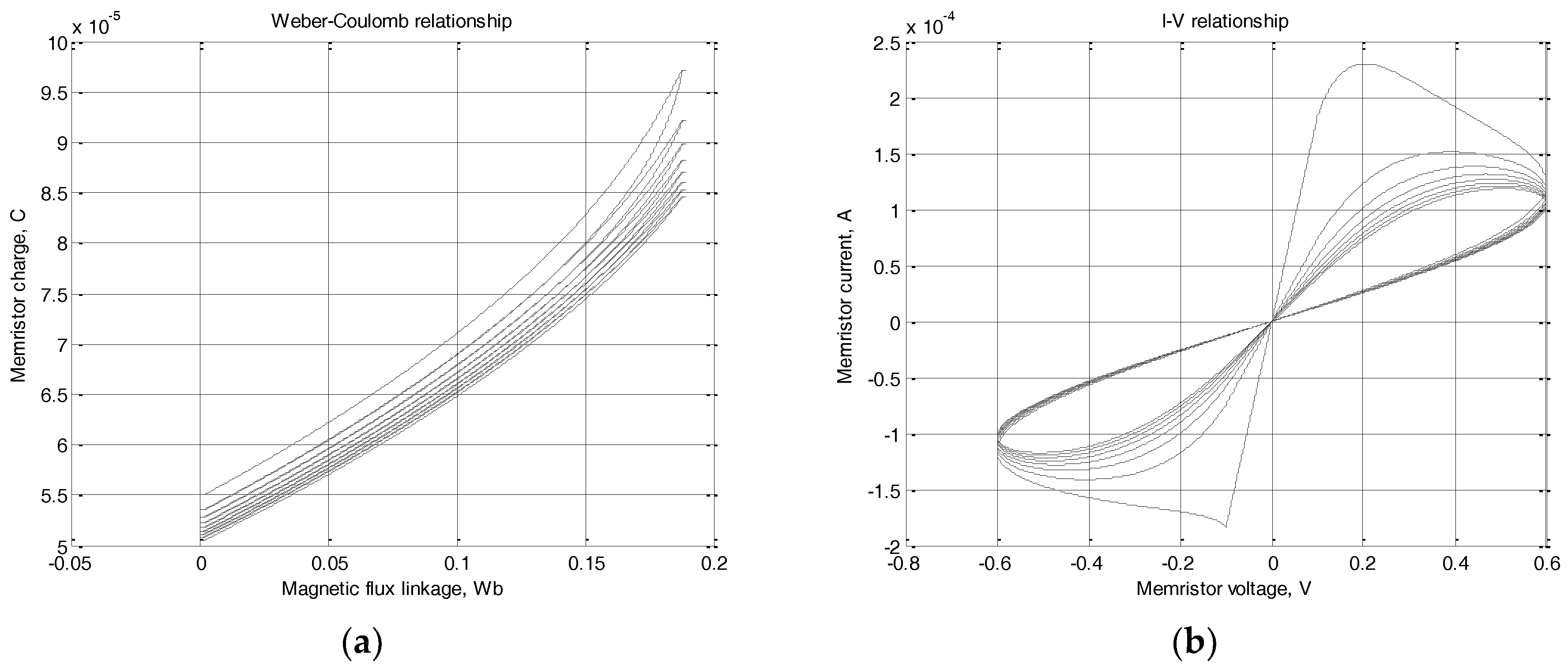
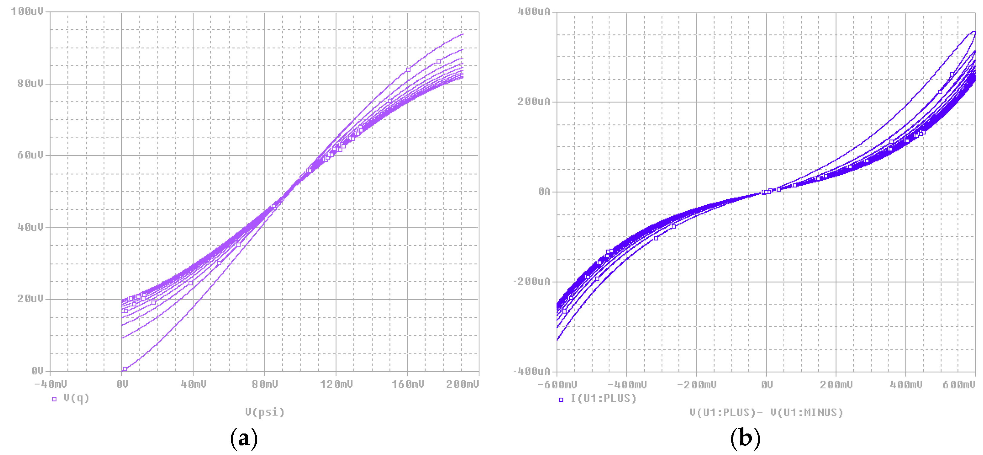
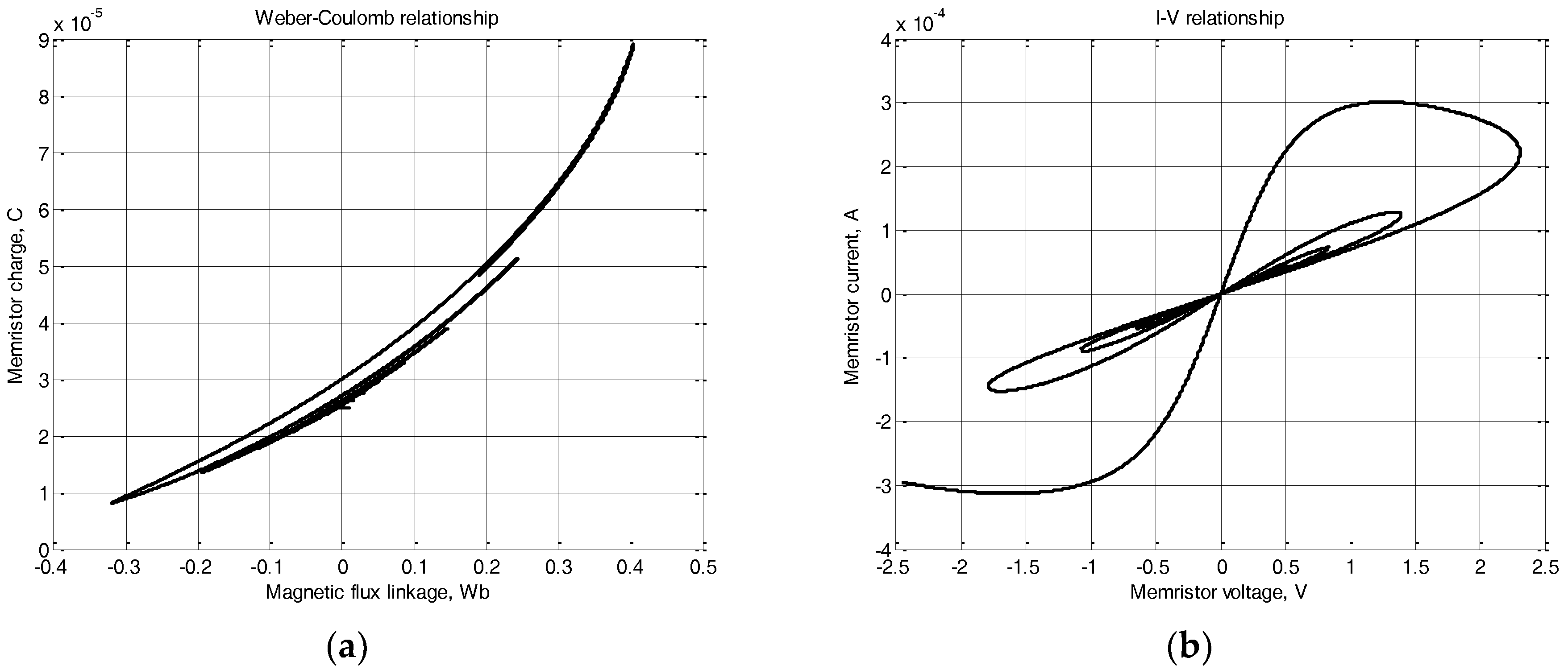
Figure 3 was the Weber-Coulomb relationship according to Pickett model and the I-V relationship of the memristor element according to Pickett model. The sinusoidal voltage signal generated by the voltage source and used for the computer simulation is:
u(t) = 0.6
∙sin(2
∙π
∙1
∙t). For the simulation OrCAD PSpice ver. 16.3 Demo was used.
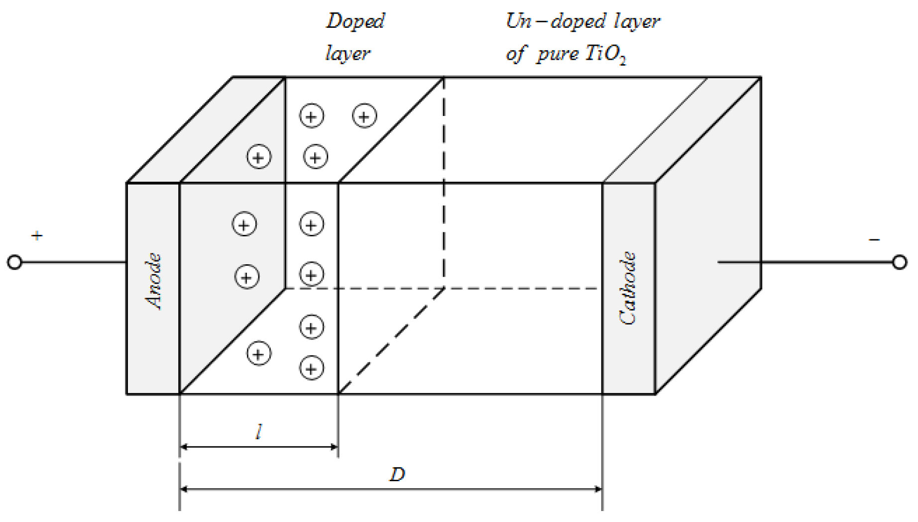
3. Basic Ideas and the Main Relationships of the Modified Biolek Model
The modified memristor model proposed here will be discussed using the titanium-dioxide memristor nanostructure described in [
2] by Strukov and Williams. A graph of the memristor structure according to the model proposed by Strukov and Williams is presented in
Figure 4. The left region of the TiO
2 memristor structure with a length of
l is partially doped with oxygen vacancies using an initial electroforming process with a high constant voltage and has low resistance [
2]. The second sub-layer of the memristor element is prepared of pure TiO
2 and it has very high resistance [
2]. The length of the whole memristor nanostructure is denoted with D and has a value of 10 nm [
2].
The normalized length of the doped layer, also known as the state variable
x of the memristor [
2,
3], could be defined with the following formula (12):
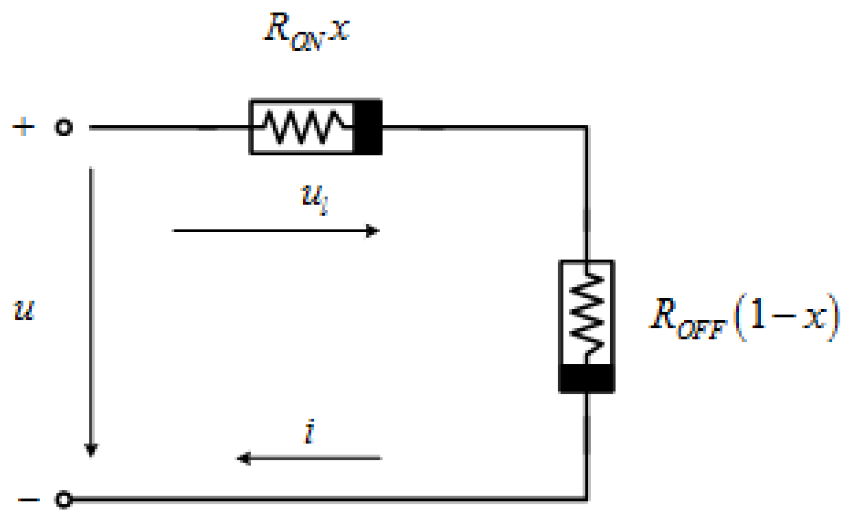
The equivalent resistance of the memristor element could be expressed using the assumption for series connection of the doped and the un-doped regions [
2,
3] and the substituting circuit given in
Figure 5:
where
RON =100 Ω and
ROFF = 16 kΩ are the memristances of the memristor for fully-closed and fully-open states [
2,
7], respectively, for
x = 1 or
x = 0.
The current-voltage relationship could be expressed using (13) and Ohm’s law [
11]:
The voltage drop across the doped region of the memristor element
ul [
11] is:
The electric field intensity in the doped layer of the memristor element
El is [
11,
12]:
The rate of moving the boundary between the doped and the un-doped layers of the memristor element [
12] is:
where
μ = 1∙10
−14 m
2/(V∙s) is the mobility of the oxygen vacancies [
2,
7]. After transformation of (17) and using (16) the following Equation (18) is derived:
where
k is a constant dependent only on memristor parameters . Using (18), the maximal amount of electric charges
qmax that the memristor accumulates could be calculated [
11] when
x = 1:
where the time for charging the memristor τ depends on the current intensity
i. Using (18) and (19) it could be derived that the electric charge accumulated in the memristor element is proportional to the maximal amount of electric charge
qmax and the state variable
x [
11]:
where in the integral in the right side of (20) the state variable
x is substituted with the variable
y, and
x is the upper limit of the definite integral. When two or more memristor elements are connected in an electric circuit [
7,
8] formula (18) is modified and Equation (21) is derived:
where
η is a polarity coefficient [
7,
8]. When the memristor element is forward-biased then
η = 1. For a reverse-biased memristor
η = −1 [
7,
8]. Formula (21) is valid only for very small electrical currents and memristor voltages [
2]. For representing the phenomenon of a nonlinear ionic dopant drift in the general case an additional nonlinear window function
f(x) has to be used in the right side of Equation (21) [
3,
6,
7] and the following formula is derived (22):
Equations (14) and (22) fully describe the general memristor model.
Several different basic window functions are used in the memristor modeling [
3,
6,
7].
A very important and frequently used window function is [
6]:
The function expressed with (23) is presented for first use by Biolek in [
6], and it is also known as a Biolek window function [
6]. The function
stp(i) [
6] used in (23) is:
After substitution of (24) [
6] in (23) the following equation is derived:
The original Biolek model [
6] is fully described with Equations (14), (22), and (25).
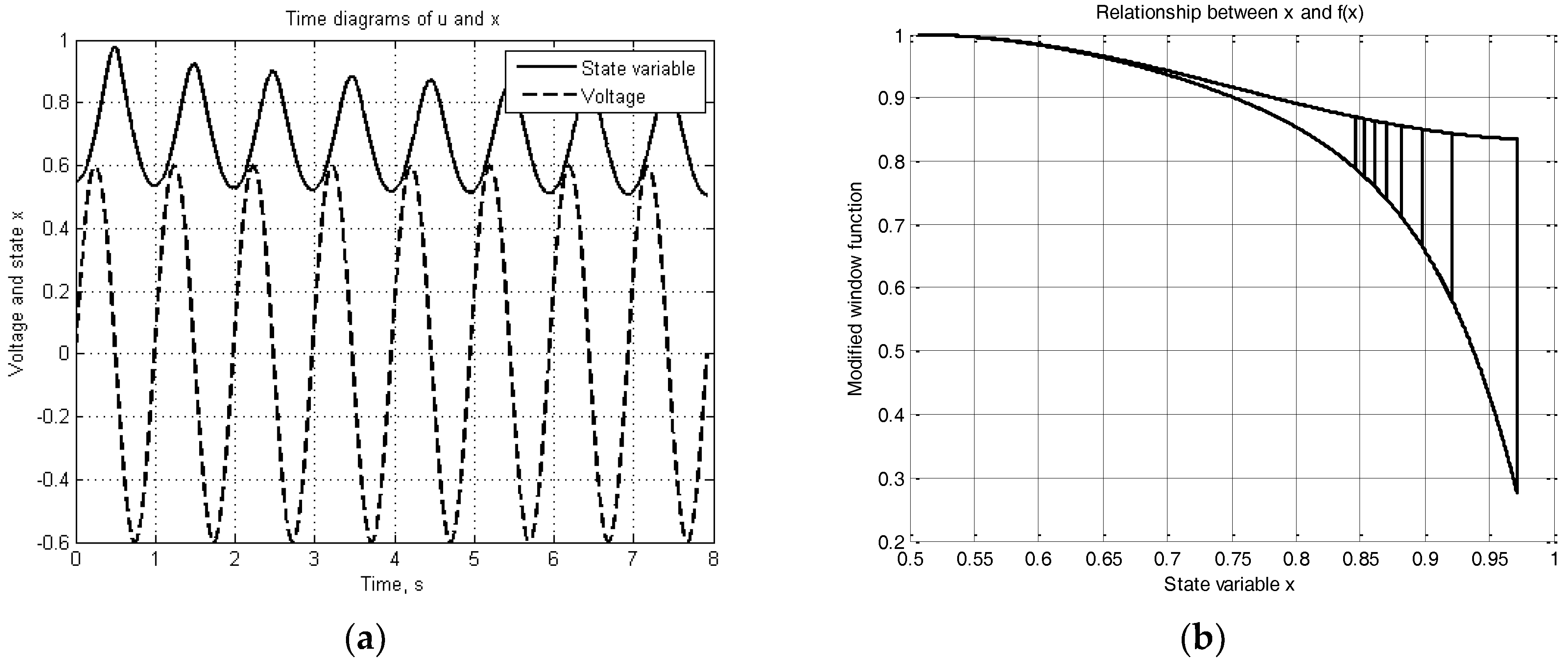
Here a simple modification of (25) is made. To increase the nonlinearity extent of the modified Biolek model, the authors proposed an additional weighted sinusoidal window function of the state variable
x:
where
m is in the interval [0, 1] and
fBM is the modified window function. The modified Biolek model proposed in this paper is fully described with the following Equation (27):
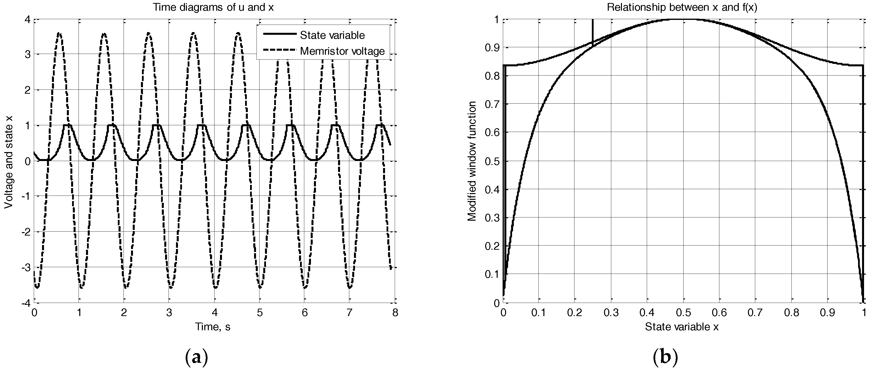
If m = 0 and if the activation threshold of the memristor uthr = 0 the modified Biolek model is transformed into the original Biolek model. So it could be concluded that the original Biolek memristor model is a special case of the modified Biolek model proposed in this paper.
6. A Comparison of the Modified Memristor Model with Existing Models
In this section a comparison of the modified Biolek model with the Joglekar memristor model [
3] for soft-switching mode will be done. According to [
3] the window function used in Equation (22) is:
Equation (28) is presented for first use by Joglekar in [
3] and it is also known as Joglekar window function [
3]. Using (14), (22), and (28) the Joglekar memristor model could be fully described with Equation (29) where the state-dependent Ohm’s Law is also included [
3].
The Joglekar memristor model could be simulated using the code given in
Section 4 but Equation (28) has to be used instead of the Biolek window function in row 6 in the code. The code of the function for calculating the state variable and the Joglekar window according to the Joglekar memristor model is presented below and it could be used by the readers for simulations [
13]:
A function for simulating the Joglekar memristor model
function [x,joglwin]=jogl(deltat,u,k,eta,deltaR,Roff,x0,N)
Parameter p=2; x=[ ];joglwin=[ ];
for n=1; x1=x0; joglwin1=1-((2*x1-1)^(2*p)); end;
for n=2:1:N+1; x1(n)=x1(n-1)+eta*k*deltat*u(n-1)*((1-(2*x1(n-1)-1)^(2*p))/(deltaR*x1(n-1)+Roff)); joglwin1(n)=1-((2*x1(n)-1)^(2*p)); end;
x=[x x1]; joglwin=[joglwin joglwin1]; end function.
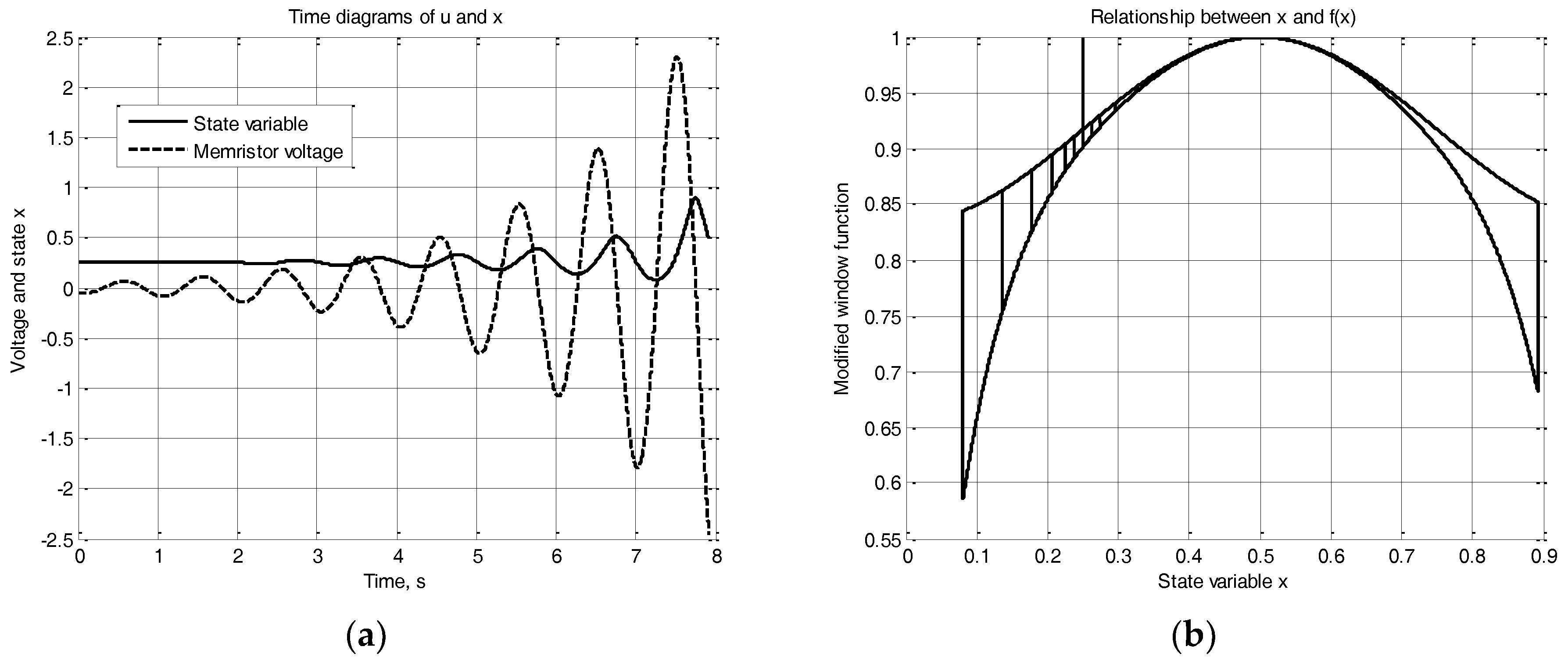
The voltage signal used for simulation of the Joglekar model and the modified model is:
u(t) = 3.3∙sin(2∙π∙2∙
t− 60°). The I-V relationships of the memristor are presented in
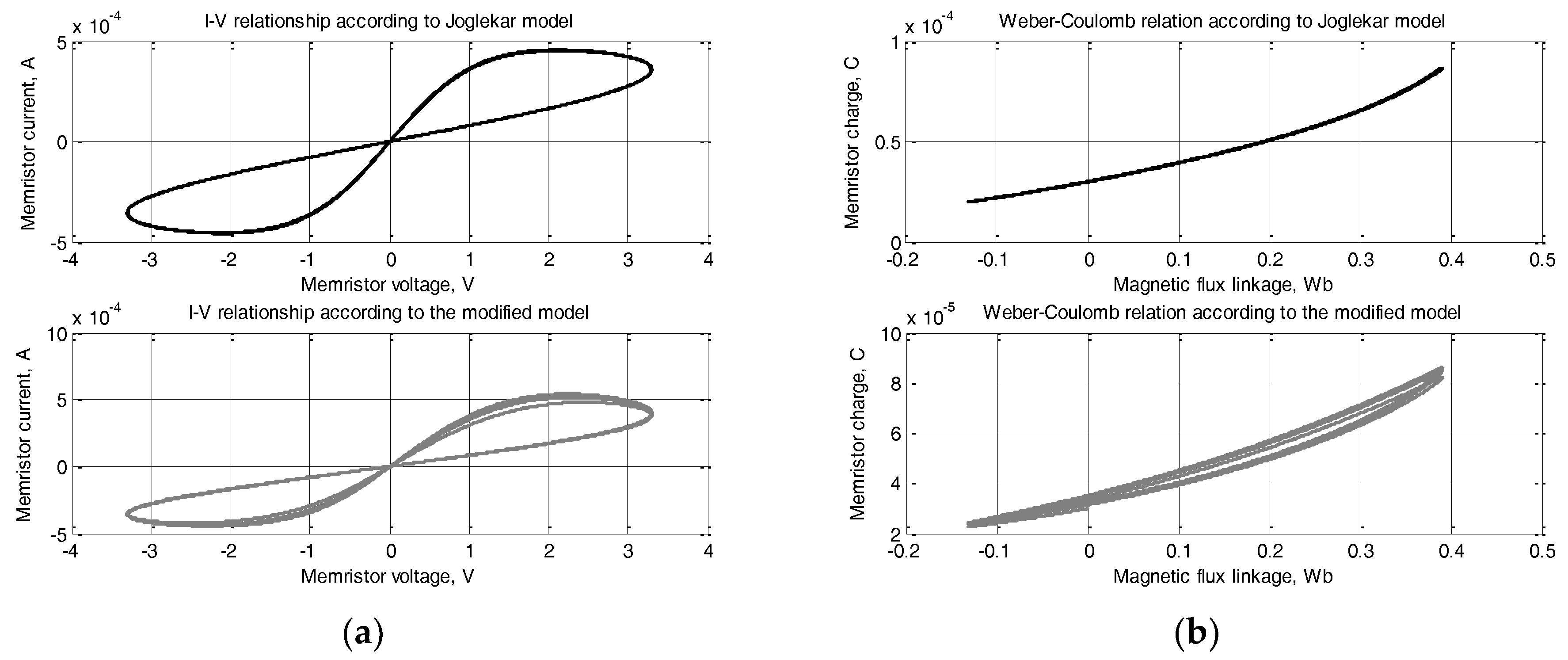
Figure 12a. In this case, the I-V curve according to Joglekar’s model is double-valued while the modified model represents multi-valued curve. The state-flux relationships are given in
Figure 12b. According to Joglekar’s model, this relation is single-valued, which is an advantage with respect to the multi-valued state-flux characteristics obtained by the modified model.
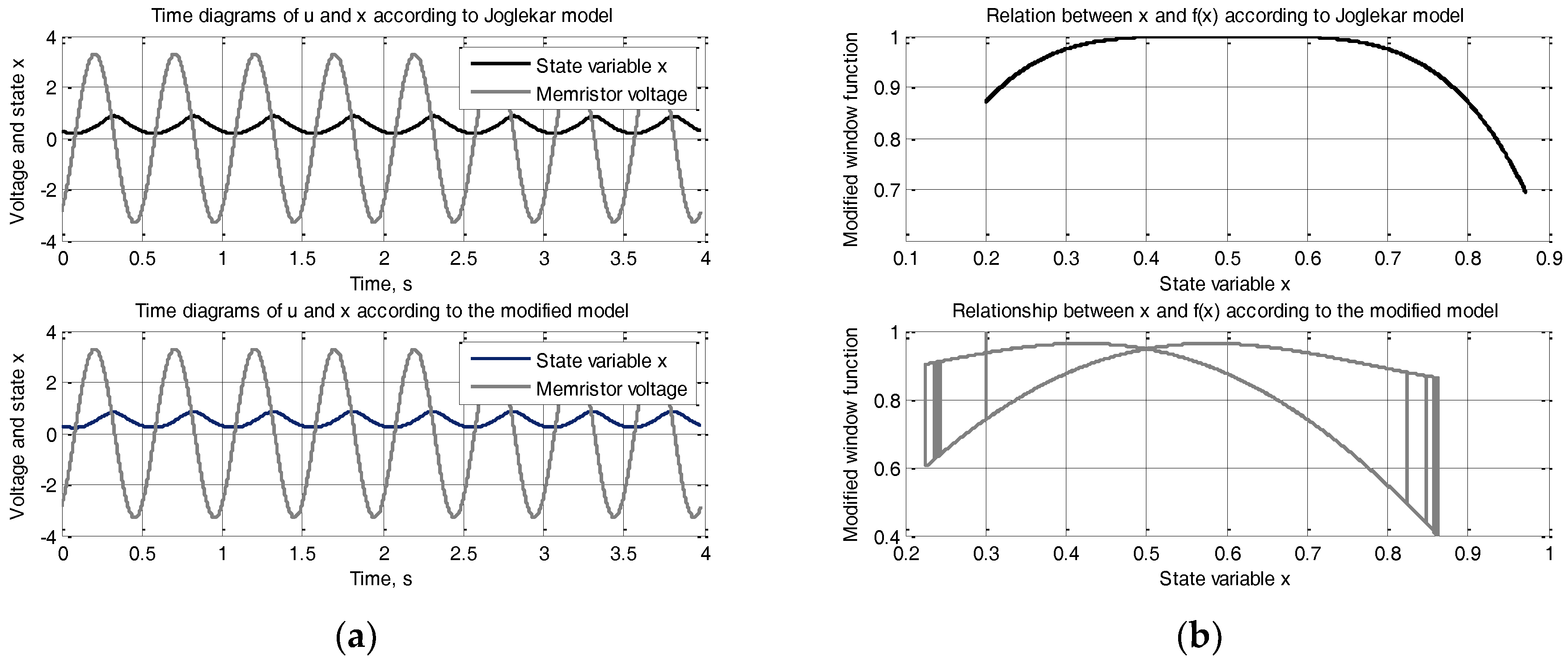
The time diagrams of the Joglekar memristor model and of the modified model presented in
Figure 13a are almost identical. The relationships between the window function values and the state variable
x for the Joglekar model, and for the modified memristor model are presented in
Figure 13b. The state variable of the memristor models changes in equivalent intervals. The modified Biolek window function in this case provides higher nonlinearity of the memristor, which is an advantage of the modified model with respect to the Joglekar model. Another advantages of the modified Biolek model proposed here is the ability for realistic representation of the boundary effects when the memristor operates in a hard-switching mode and the use of sensitivity threshold. The original Joglekar memristor model does not have mechanism for representing the boundary effects and it is appropriate only for simulating of memristors for soft-switching mode.
7. Conclusions
After finishing the adjusting process of the modified Biolek model and obtaining the basic results, several conclusions could be made. The modified memristor model based both on Biolek model and GBCM model is a general one and it contains a modified window function, which is a sum of the original Biolek window function, and a weighted sinusoidal window function. In the special case when the coefficient in front of the sinusoidal window function and the activation threshold are chosen to be equal to zero, the original Biolek memristor model is obtained. If the modified model presented here is adjusted, we could obtain results identical to those obtained by the Pickett model. Of course, the results obtained in the present research are not exactly the same like those produced by Pickett model, which has the highest accuracy but also has many convergence problems and is not appropriate for simulations. The main advantage of the modified Biolek model with respect to the Pickett model is the lack of convergence problems and the possibility for use of the modified model for computer simulations of memristors and memristive circuits.
The modified memristor model proposed here was compared with Joglekar memristor model for soft-switching mode. The state-flux relationship obtained by Joglekar model is a single-valued curve, which is an advantage of Joglekar model with respect to the modified model which state-flux characteristics are multi-valued. On the other hand, the modified memristor model proposed in this paper has several advantages with respect to Joglekar memristor model—higher nonlinearity of the dopant drift, ability for realistic representation of the boundary effects, and the use of sensitivity voltage threshold. After comparison of the modified memristor model proposed in this paper with the Pickett model it could be concluded that the Pickett model could be simulated for a narrow range of voltages and for higher voltages convergence problems occur. During the tests of Pickett model only operation in a soft-switching mode was observed. An advantage of the model proposed in this research with respect to the Pickett model is the possibility for simulating the modified model in a broaden voltage range and the observation of hard-switching mode behavior.


