All articles published by MDPI are made immediately available worldwide under an open access license. No special
permission is required to reuse all or part of the article published by MDPI, including figures and tables. For
articles published under an open access Creative Common CC BY license, any part of the article may be reused without
permission provided that the original article is clearly cited. For more information, please refer to
https://www.mdpi.com/openaccess.
Feature papers represent the most advanced research with significant potential for high impact in the field. A Feature
Paper should be a substantial original Article that involves several techniques or approaches, provides an outlook for
future research directions and describes possible research applications.
Feature papers are submitted upon individual invitation or recommendation by the scientific editors and must receive
positive feedback from the reviewers.
Editor’s Choice articles are based on recommendations by the scientific editors of MDPI journals from around the world.
Editors select a small number of articles recently published in the journal that they believe will be particularly
interesting to readers, or important in the respective research area. The aim is to provide a snapshot of some of the
most exciting work published in the various research areas of the journal.
Department of Electronic Apparatus Design, Institute of Nanotechnology, Electronics, and Electronic Equipment Engineering, Southern Federal University, 2 Shevchenko St., Taganrog 347922, Russia
*
Author to whom correspondence should be addressed.
In this paper, we consider the problem of the research and development of high-speed semiconductor photodetectors suitable for operation as parts of on-chip optical interconnections together with the high-speed laser modulators based on the AIIIBV nanoheterostructures. This research is aimed at the development of the models and modelling aids designed for the simulation of carrier transport and accumulation processes taking place in on-chip photosensitive devices during the detection of subpicosecond laser pulses. Another aim of the paper is to apply the aforementioned aids for the investigation of GaAs p-i-n and Schottky-barrier photodiodes. We propose the non-stationary drift-diffusion models, an original numerical simulation technique and the applied software allowing one to simulate the photosensitive devices with different electrophysical, constructive and technological parameters. We have taken into account different kinds of carrier generation and recombination processes, the effects of electron intervalley transition and carrier drift velocity saturation in order to improve the simulation results’ adequacy. We have concluded that the influence of these effects on the performance of photodetectors for on-chip optical interconnections is significant. The response time of GaAs p-i-n and Schottky-barrier photodiodes calculated taking into account the drift velocity dependence on electric field intensity is insufficient for the adequate detection of subpicosecond laser pulses. According to the simulation results, it is reasonable to develop the methods aimed at the increase in the drift velocity of charge carriers in the photodetector active region by means of built-in electric field reduction.
The problem of interconnection performance buildup is one of the key problems of modern micro- and nano-electronics. Metal conductors have been used for the interconnecting of integrated circuit (IC) elements since the early days of microelectronics. According to the forecasts of experts, traditional conductors will cease to meet the increasing requirements for the channel capacity, energy efficiency, noise immunity, reliability and manufacturability of integrated interconnections in the immediate future [1]. Integrated electronics will achieve the physical limit of device development called the “interconnection bottleneck” [2]. Nowadays, scientists research different ways of the problem solution [3,4,5,6]. The implementation of the promising approaches will lead to the sustainable development of integrated electronics in the future.
Optical interconnecting of IC elements is one of the advanced conceptual methods aimed at the solution of the problem being considered [7,8,9]. The majority of experts believe that this concept has a real chance to improve the performance of ICs. The optoelectronic approach has some geometrical, design, parametrical, technological and economic advantages over its counterparts. In the near future, ICs with optical interconnections will be implemented on the basis of traditional electronic elements. Most interconnections in such devices will be realized as traditional metal conductors. Constructively- and technologically-integrated optical interconnections will replace conductors with critical parameters.
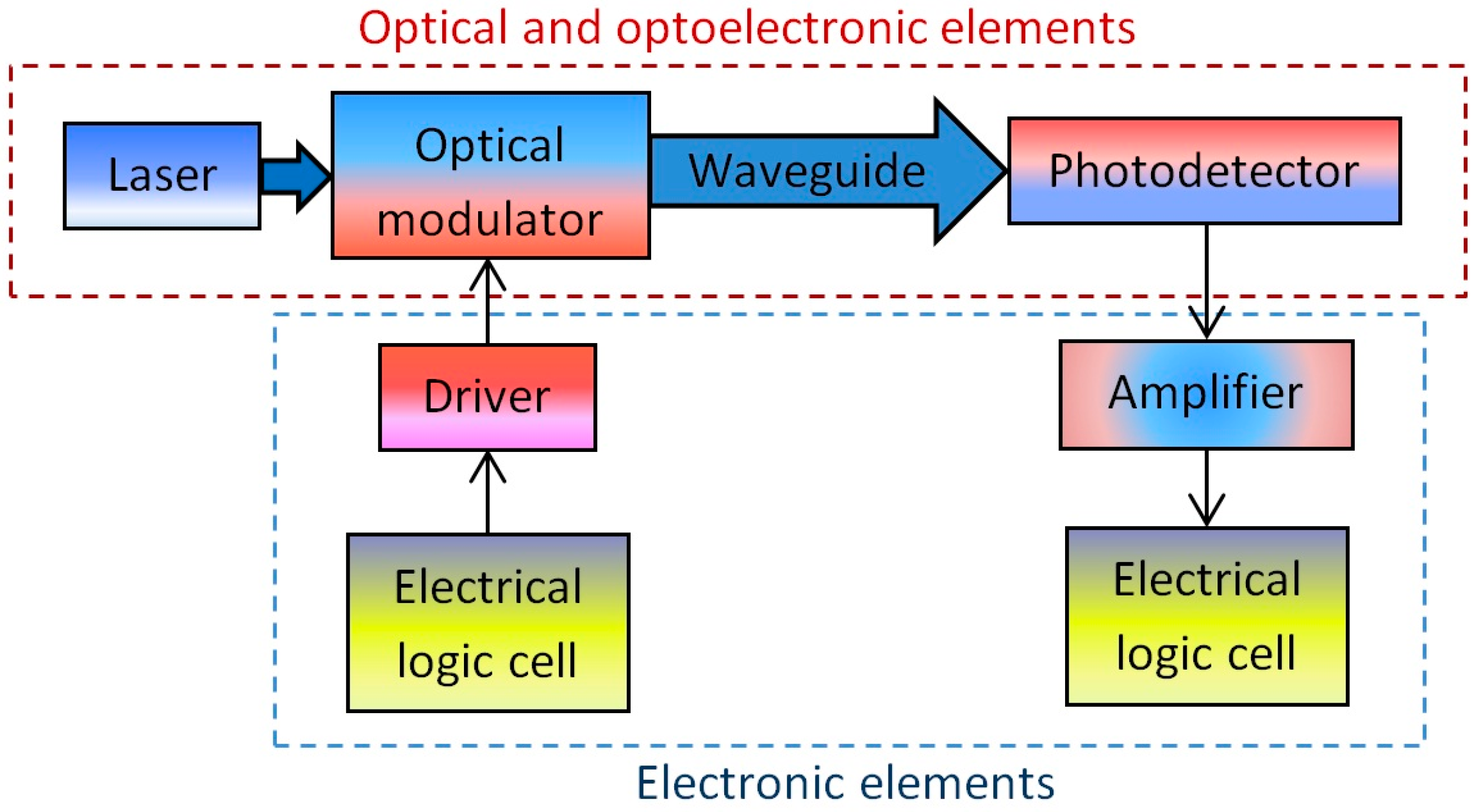
On-chip optical interconnection is a conceptual functional unit of next-generation IC. This unit provides the conversion of electric signals to optical ones, their transmission between on-chip elements and the inverse signal transformation for the processing of transmitted data by electronic elements of IC. The structure chart of typical on-chip optical interconnection is shown in Figure 1. Generally, this device consists of the following basic elements [10]:
a source of optical radiation (laser);
a high-speed modulator;
an integrated waveguide;
a photodetector;
special circuits for the processing of control and sensing electric signals.
Complex systems additionally include integrated optical switchers, deflectors, coupling elements, multiplexers, optical amplifiers, waveguide splitters, lenses and other optical elements. Full or partial constructive and technological integration with other elements of IC is the main attribute of on-chip optical interconnection. It is expected that the next-generation ICs with both electrical and optical interconnections will have the optimal balance between technical, technological and economic parameters.
Currently, the problem being considered is relevant for the developers of multi-core ultra-large-scale integrated circuits (ULSIs). The implementation of the modern trend of ULSI development, including the integration level and chip area growth, transistor downsizing and increase in the core number, results in the following challenges:
complexification of the interconnection system;
increase in the length of inter-core connections;
interconnection density growth.
The influence of the represented challenges on the ULSI performance is significant. The promising way of the problem solution is the development of multi-core systems with optical inter-core connections. Silicon digital cores fabricated using traditional techniques are interconnected optically in such devices.
There are many conceptual methods designed for the implementation of optical interconnecting for advanced ICs. According to these concepts, we assume that traditional electronic elements, including complementary metal-oxide-semiconductor (CMOS) transistors, remain unchanged in general. Differences between them are related to the choice of the basic material for integrated optoelectronic elements.
Many papers are aimed at the implementation of silicon and silicon-germanium on-chip optical interconnections [11,12,13]. This concept seems to be optimal in terms of IC manufacturability. However, today, it is problematic to fabricate high-efficiency integrated lasers from the materials being considered. This fact is a significant drawback of this concept.
The high performance of AIIIBV optoelectronic devices determines the development of the opposite concept of on-chip optical interconnecting [14,15,16]. This concept is aimed at the constructive and technological integration of silicon CMOS elements with the optical interconnections based on AIIIBV compounds. Obviously, the implementation of the aforementioned concept will lead to the complexification of IC fabrication flow in comparison with traditional integrated devices. However, significant results have already been achieved in the field of the epitaxial growth and other techniques of the integration of AIIIBV layers with silicon substrates [17,18,19]. The evolution of such technology will allow one to manufacture both electronic and optoelectronic units of the advanced ICs during the unified fabrication cycle. It will cause the economic efficiency of these devices in the case of their mass production. Furthermore, the technological compatibility of optical interconnections with the next-generation high-speed electronic elements based on AIIIBV heterostructures is the advantage of the concept being considered. These devices can be applied for the implementation of laser drivers and circuits for the processing of photodetector sensing signals.
In this paper, we consider the promising concept of the application of injection lasers with double AIIIBV heterostructures and functionally-integrated modulators as basic optoelectronic elements of optical interconnections for multi-core ULSIs [20,21,22]. According to the results of the numerical simulation, the modulation frequency of optical signals in such devices can reach the value of 1 THz and above. Theoretical analysis of the features of optical interconnections based on the laser modulators shows that these systems have potential advantages over traditional metal interconnections and certain optical analogues. The advantages will provide the high performance, industrial and economic efficiency of the next-generation ULSIs with AIIIBV optical interconnections. Such optical systems can be implemented as parts of digital ICs, as well as microwave integrated devices.
The development of high-speed photodetectors suitable for the operation as parts of on-chip optical interconnections together with the laser modulators is the important problem of the scientific field being considered. The essential requirements to these photosensitive devices are the following:
manufacturing capability with the other optoelectronic elements of on-chip optical interconnections;
performance sufficient for the adequate detection of modulated optical signals.
Thus, the photodetectors of the high-speed optical interconnections should be implemented on the basis of AIIIBV semiconductor materials and provide the detection of subpicosecond laser pulses. The analysis of transients taking place in on-chip photodetectors during the detection of subpicosecond laser pulses is a cutting-edge research direction. Different scholars consider the performance of semiconductor photodetectors in some papers (for example, in [23,24,25]). They view the detection of optical pulses lasting much longer than 0.1 ps.
This paper is aimed at the following:
the development of models and simulation aids for the research of transients taking place in photodetectors for on-chip optical interconnections during the detection of subpicosecond laser pulses;
their application for the simulation of the basic types of integrated photodetectors: p-i-n structures and Schottky-barrier photodiodes.
In this paper, we propose to utilize numerical models based on the drift-diffusion equation system for the simulation of charge carrier transport and accumulation in on-chip photodetectors. Such models can be described as research tools providing the optimal balance between the adequacy and accuracy of simulation results and the complexity of their obtainment. The drift-diffusion models allow one to take into account some physical effects whose simulation within other methods is problematic. In spite of several limitations, this type of model remains one of the most effective tools for the research of semiconductor devices [26]. We have successfully applied the drift-diffusion equations for the analysis of dynamical processes taking place in semiconductor injection lasers with functionally-integrated modulators [27].
2. Models and Simulation Methods
As noted above, in this research, we consider the models of photodetectors for on-chip optical interconnections. These models are based on the drift-diffusion equation system [28]. It can be written in the following general form:
where , are the electron and hole concentrations; , are the electron and hole mobilities; is time; is the elementary charge; is the electrostatic potential; is the temperature potential; is the generation rate of electron-hole pairs; is the recombination rate; is the dielectric permittivity of semiconductor; is the permittivity of vacuum; , are the concentrations of the ionized donors and acceptors.
In this paper, we analyze the photoconductive operation mode of photodetectors providing the current output signal and faster response time than the photovoltaic one. The following Dirichlet boundary conditions are obtained for the photoconductive mode assuming the infinite recombination velocity at the contact [29]:
for the ohmic contacts:
for the Schottky contacts:
where is the intrinsic carrier concentration; is the bias voltage applied to the contact at the moment ; is the Schottky barrier height.
The numerical solution of the stationary drift-diffusion equation system is a reasonable way to calculate the adequate initial conditions. We apply the standard Gummel iteration method [30] and traditional Slotboom formulation [31] for this purpose.
We take into account the generation and recombination of charge carriers in the photodetector regions using the following analytical models:
the Shockley–Read–Hall model of the carrier trap recombination applicable for the regions with impurity conductivity [32]:
where , are the electron and hole lifetimes; , are the effective densities of states in the conduction and valence bands; , are the energy levels of the conduction band bottom and valence band top; is the trap energy level; is the Boltzmann constant; is the temperature of the semiconductor;
the model of the direct radiative recombination suitable for the regions with intrinsic conductivity [32]:
where is the bimolecular recombination coefficient calculated using the Garbuzov formula [33]:
where is the energy gap of the semiconductor;
the model of the band-to-band Auger recombination/generation [32]:
where , are the Auger coefficients for electrons and holes;
the model of the bipolar optical generation:
where is the quantum efficiency of the photodetector; is the volume power density of the incident optical radiation at the moment ; is the photon energy of the incident radiation.
Equation (16) is obtained under the assumption that the optical generation rate does not depend on the coordinate. It corresponds to the integral approach to the description of the optical radiation absorption by the material of photodetector active area. Variable defines the external quantum efficiency of the photodetector. It is given by:
where is the internal quantum efficiency, which describes the number of electron-hole pairs generated by one absorbed photon; is the radiation power absorbed by the photodetector active region; is the total power of the incident radiation.
In this paper, we consider resonant cavity-enhanced photodetectors. If , the peak quantum efficiency of such devices at the resonance wavelengths can be calculated as follows [34]:
where , are the reflection coefficients of cavity mirrors; is the resonator length; is the absorption coefficient of the active region material.
The value of quantum efficiency calculated using Equation (18) corresponds to the following resonance condition [35]:
where is a positive integer; is the wavelength of optical radiation in the resonant cavity material.
In this research, we take into account the dependence of carrier mobility on the temperature and impurity concentration applying the following low-field analytical model [36]:
where is the conductivity type of semiconductor (n or p); ; ; , , , , and are the parameters depending on the properties of the semiconductor material.
In this paper, we address the influence of the physical effect of electron intervalley transition on the electron drift velocity in multivalley AIIIBV semiconductor materials. This effect causes the dependence of electron mobility on the electric field intensity and can affect the characteristics of AIIIBV devices significantly. We apply the simplified model describing the stationary distribution of electrons between two valleys of the semiconductor (for example, Γ and L in GaAs). The average electron drift velocity can be estimated assuming the equality of the electron temperature in valleys.
The appropriate equations have the following form [37]:
where is the electric field intensity; is the electron temperature; is the energy relaxation time; is the electron mobility in the lower valley (Γ for GaAs) calculated using Equations (20) and (21); is the energy difference between the valleys; is the ratio between state density in the upper valley and the lower one calculated utilizing the following equation [37]:
where , are the numbers of upper and lower valleys; , are the effective masses of electrons in the corresponding valleys; for GaAs, , , , ( is the free electron mass); hence, [37].
The model described by Equations (22)–(24) allows one to obtain the adequate results only for the rather weak electric fields, because it does not take into account the effect of electron drift velocity saturation. If the intensity of the electric field is sufficient for the electron drift saturation, it is reasonable to define the average carrier velocity as the saturation velocity for the semiconductor material. In this paper, we propose to apply the linear approximation of the experimental data, which were obtained by other authors for a field intensity higher than 20 kV/cm [38].
We also take into account the effect of hole drift velocity saturation. We apply the analytical model for GaAs proposed in [39]. This model is the approximation of Monte Carlo simulation results. It is given by the following equation:
where is the average hole drift velocity; is the hole saturation velocity; is the low-field hole mobility calculated using Models (20) and (21); .
We utilize the following equation expressing the ratio between the saturation drift velocities of electrons and holes in a semiconductor to calculate :
where is the electron saturation velocity; , are the effective masses of electrons and holes. We obtained Equation (26) under the assumption that electron and hole saturation velocities correspond to the excitation energy of the optical phonon.
Equations (20)–(26) describe the stationary states. Photodetector illumination leads to the growth of carrier concentrations. However, it does not result in the detectable change of the distribution of electric field intensity in device structure. Therefore, the dynamic nature of the high-field effects can be neglected.
Variables , and are included in the drift-diffusion model as follows. Formula (22) is the transcendental equation solvable for electron temperature . This equation describes the dependence of on electric field intensity . We calculate solving Equation (22) numerically at known values of its parameters. Then, we input the electron temperature into Formula (23) and compute average electron drift velocity . We utilize the definition of carrier mobility to make the transition from to electron mobility :
We calculate average hole drift velocity applying Equation (25) and the additional Formula (26). In these equations, all parameters are known. We compute hole mobility in a similar way to the electron one:
Variables and are the parameters of the drift-diffusion Models (1)–(3).
We apply the following algorithm for the calculation of carrier mobilities during the numerical simulation of photodetectors. We compute and dependences using Equations (22)–(24), (27) and Equations (25), (26), (28) before the solution of the drift-diffusion equation system. The range of electric field intensity corresponds to the photosensitive devices being considered. Further, we solve the stationary problem applying low-field mobility Models (20) and (21) and get intermediate simulation results, including the distribution. This distribution and previously computed and dependences are utilized for the calculation of the and distributions. We apply these data to solve the stationary problem again and get initial conditions. Thereafter, and are additionally refined. We assume that the and distributions are constant during the solution of non-stationary problem. This is caused by the fact that we consider illumination transients. Such processes do not lead to the noticeable changes of the distribution.
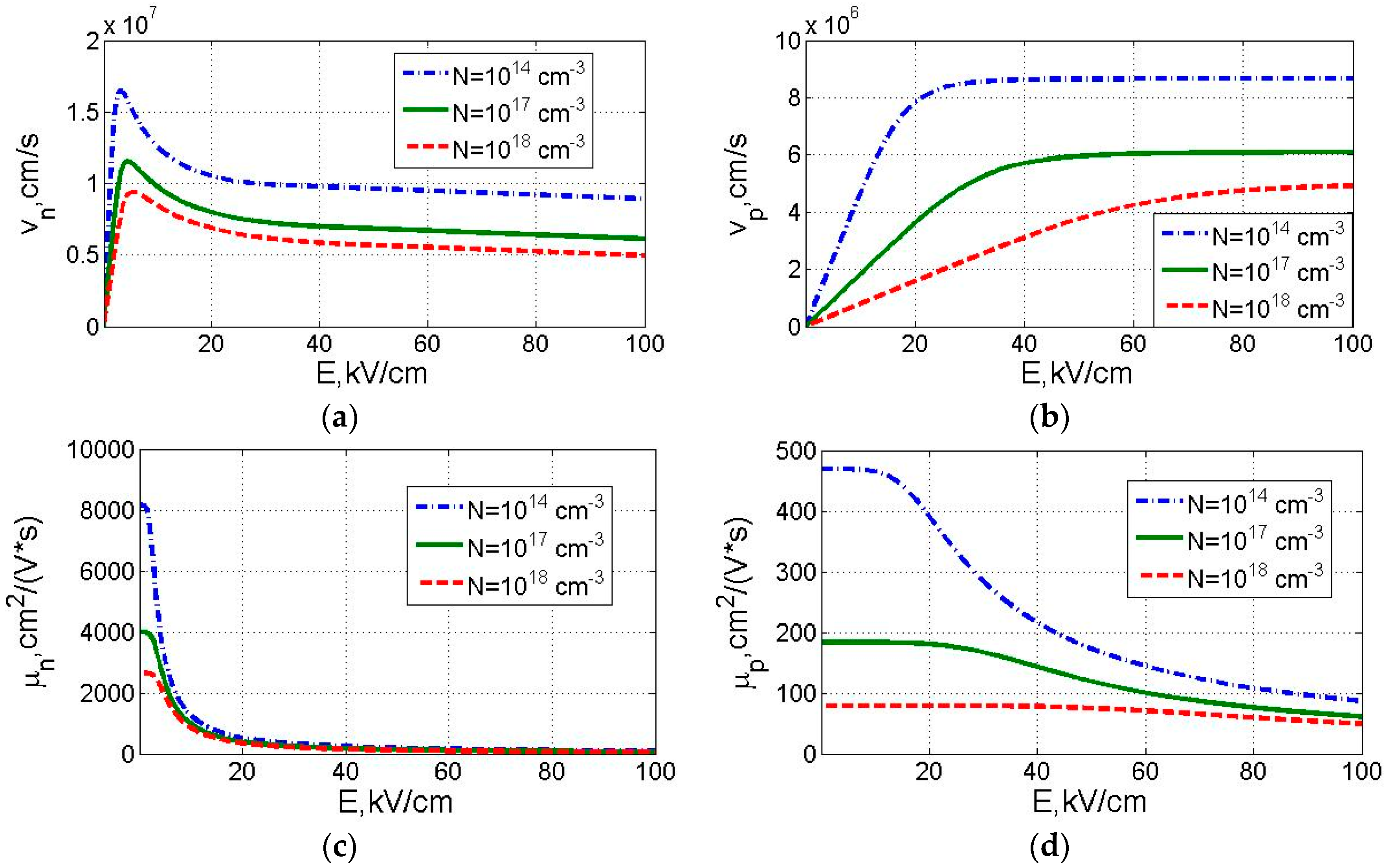
Figure 2 shows the dependences of carrier drift velocities and mobilities in GaAs on the electric field intensity. We calculated these curves using the aforementioned models at different impurity concentrations. The graphs show the qualitative correspondence with the experimental data and Monte Carlo simulation results represented in the papers [40,41]. According to the curves, the growth of the electric field intensity in GaAs leads to the significant reduction of carrier mobilities. Thus, we can make the following conclusion. The effects of electron intervalley transition and carrier drift velocity saturation can affect the performance of GaAs diodes because such devices are characterized by the intense built-in electric field (about several tens of kV/cm and above).
The implementation of drift-diffusion Models (1)–(3) with Boundary Conditions (4)–(9) and parameter Models (10)–(26) is possible within the numerical methods of mathematical physics only. Some challenges are typical for the non-stationary numerical simulation of semiconductor devices. These challenges are:
the numerical instability of solution schemes;
the inadequacy of simulation results caused by calculation error.
In our opinion, a universal approach to the solution of these problems has not been developed yet. Some researchers omit the important information about the implementation of models and methods proposed in their scientific papers. That is why sometimes, it is difficult to reproduce such tools and to use them efficiently in your own research. Standard commercial software for the simulation of semiconductor devices is quite expensive. Usually, it is not reasonable to apply such software for the solution of special scientific problems. The aforementioned features determine the relevance of the development of modelling methods and aid simulating semiconductor devices within the drift-diffusion formulation.
We consider the finite difference numerical method [28] in this paper. There are various difference methods suitable for the discretization of time derivatives included in continuity Equations (1) and (2). We propose to apply the explicit one [42] in combination with the Gummel iteration method for the drift-diffusion simulation of high-speed photodetectors. This approach allows one to simplify the implementation of the drift-diffusion numerical models significantly.
If we use the explicit method together with the Gummel one, the right sides of the continuity equations are defined by the values of decision variables at the current (j-th) instant of time. This means that we calculate carrier concentrations at the next (j + 1)-th instant of time by performing some rather simple mathematical operations. In this case, the problem of non-stationary simulation is reduced to the computation of carrier concentrations and the solution of one linear equation system in every iteration step. The aforementioned linear equation system results from the discretization and linearization of the Poisson equation.
If we apply the implicit or Crank–Nicholson method under the conditions stated above, the right sides of the continuity equations include the unknown values of decision variables at the next (j + 1)-th instant of time. That is why we solve two additional linear equation systems corresponding to the discretized continuity equations for the calculation of carrier concentrations at the (j + 1)-th instant of time. The solution of the third linear equation system is necessary for the computation of the electrical potential distribution determined by the Poisson equation. Hence, the implementation of the explicit difference scheme requires three times less computational and time resources than the implicit and Crank–Nicholson ones in the case of the Gummel method application.
According to the theory of difference schemes, the implicit and Crank–Nicholson methods are characterized by the absolute numerical stability [42]. The explicit one is numerically unstable in some cases [42]. The concept of stability is applicable to the finite difference scheme, as well as to the algorithm of the numerical problem solution. The application of the stable scheme within the unstable algorithm can lead to inadequate numerical simulation results. The algorithm can demonstrate the stability in combination with the certain difference scheme, as well as the instability with another one.
As noted above, in this paper, we research the detection of subpicosecond laser pulses. This means that we consider rather short time intervals with the duration of about several tenths of a picosecond. That is why we can choose the short time step as being sufficient for the numerical stability of the explicit difference scheme. In this research, the time grid step has the value of the order of 0.1 fs.
The stability of the explicit difference scheme can be identified using the one-dimensional Courant–Friedrichs–Lewy (CFL) condition [43]:
where , are the time and coordinate grid steps; u is the velocity of carrier transport; C is the Courant number depending on the form of equation and the values of its parameters. We obtain assuming , , . This result corresponds to the problem being considered and indicates the theoretical stability of the explicit difference scheme.
Our numerical experiments show the stability of the explicit difference scheme and the algorithm of the Gummel method within the problem being considered, as well as some analogous problems of semiconductor device simulation. That is why we can regard this technique as the conditionally-stable method at a time grid step of 0.1 fs and other terms of the particular numerical problem. In spite of a very small time step, we achieve a short enough computation time for the maintenance of the simulation results’ adequacy. This fact is caused by the application of the explicit scheme together with the Gummel method. Furthermore, it should be taken into account that a small time step provides a higher accuracy of simulation results than a large one in any case.
In this paper, we do not assert the superiority of the explicit difference scheme over its counterparts in all instances. We consider the efficiency of the difference scheme application within the algorithm of the Gummel method chosen for the numerical simulation. The explicit difference scheme has more preferential than its analogues in the case being considered because it requires less time and computational resources.
The photoconductive operation mode of on-chip photodetectors is characterized by the constant reverse bias. This means that the minority carrier concentrations in the device regions differ from the majority ones by several orders of magnitude in the case of illumination absence. This results in error accumulation leading to the emergence of negative carrier concentrations during the numerical calculations. This problem can be solved by means of the improvement of the discretization scheme for differential equations. The application of the Scharfetter–Gummel approximation is a traditional approach to the problem solution [44,45].
We tried to utilize the classical Scharfetter–Gummel scheme for the simulation of high-speed photodetectors. There were some problems connected with the emergence of negative carrier concentrations during the application of this method, as well as the traditional formulation in terms of . Perhaps, it is determined by the features of the chosen algorithm of the Gummel iteration method. In this research, carrier concentrations are varied within a quite wide range. The difference between the minimum and maximum values of concentrations is about several tens of orders. That is why the choice of the optimal scale factor for the concentration is problematic.
We propose to solve the aforementioned problem by means of the application of the numerical simulation technique characterized by the following key features:
all variables in the drift-diffusion equation system are normalized using the standard scaling factors represented in [45];
sets of variables are used in Equations (1)–(3) to simplify the finite difference scheme: the left sides of Equations (1) and (2) and Equation (3) as a whole are considered in terms of ; the right sides of Equations (1) and (2) are considered in terms of , where and are the exponents of quasi-Fermi levels for electrons and holes given by the following equations [46]:
Thus, the drift-diffusion equations are considered in terms of the combined variable base ;
the discretization of the right sides of Equations (1) and (2) is implemented applying the first-order upwind scheme [47];
the direct method is utilized for the solution of linear equation systems.
We do not pretend to the universality of this simulation technique. However, we applied the developed approach for the research of some optoelectronic semiconductor devices and got adequate simulation results. The proposed technique overcomes the Scharfetter–Gummel method only within the specific problem of photodetector simulation in the case of the certain algorithm application. We do not eliminate the following fact. Under different conditions, the Scharfetter–Gummel scheme can surpass our approach in the adequacy and accuracy of simulation results.
We obtain the following non-stationary one-dimensional finite difference equations applying the aforementioned numerical simulation technique:
where is the index of coordinate grid points; is the index of time grid points; is the i-th coordinate grid step; is the j-th time grid step; is the Heaviside step function. The presence of the Heaviside function in finite difference continuity Equations (32) and (33) is caused by the application of the upwind method.
As was mentioned above, in this paper, we consider the photovoltaic operation mode. This means that photodetectors have the current sensing signal. Consequently, it is necessary to provide the acceptable adequacy of the current density calculation results in order to improve the model performance. Traditional drift-diffusion current density formulas are often used in numerical models. These equations have the following form [45]:
where , are the electron and hole current density components.
Slotboom proposed the following current density equations in terms of in the paper [31]:
In this paper, we utilize the Slotboom equations for current density computation instead of the traditional drift-diffusion Formulas (35) and (36). This is caused by the inadequate current density bursts observed on the device junctions after the end of the supply transient process in the case of the classical approach application. Obviously, the current density in all points of the semiconductor device must be equal at steady state. There is one member combining the diffusion and drift components of current density in the Slotboom formulation. It allows one to avoid the problem of the matching carrier concentrations and their gradients. The application of the current density formulas in terms of reduces the maximum error by 11 orders of magnitude and provides the adequacy of the simulation results in contrast with the classical drift-diffusion formulation.
We do not assert that the Slotboom equations always provide more adequate results than the drift-diffusion ones. However, the application of the Slotboom formulation allows one to improve the adequacy of the calculation of the current density spatial distribution within the numerical problem being considered.
We calculate the full current density taking into account the electron and hole current components and the Maxwell displacement current . The latter is associated with the detector capacitance and computed as follows [39]:
where is the electric field intensity vector.
We developed specialized applied software in the GNU Octave program using the MATLAB programming language. This software implements the aforementioned models and numerical technique for the simulation of on-chip p-i-n structures and Schottky-barrier photodiodes with different electrophysical, constructive and technological parameters.
3. Simulation Results and Discussion
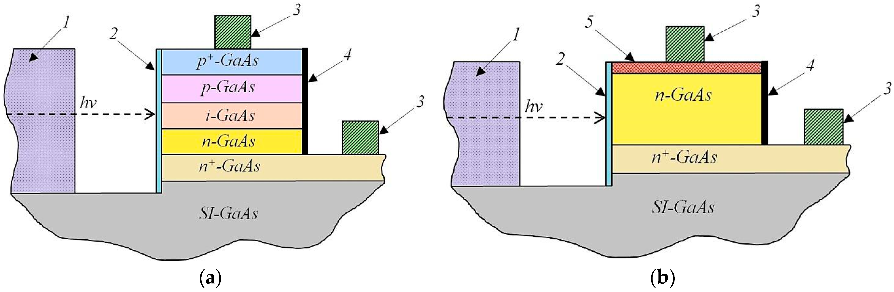
In this paper, we consider the numerical drift-diffusion simulation of GaAs p-i-n and Schottky-barrier photodiodes for on-chip optical interconnections. Figure 3 shows the structures of the researched photodetectors. Impurity concentrations in the regions of photodiodes are given in Table 1. P+ and n+ regions ensure the ohmic contacts between conductors and device regions. We have researched Schottky-barrier photodiodes with both n- and p-type near-contact regions. The structure of the p-type Schottky-barrier photodiode is analogous to the one represented in Figure 3b.
There are etched areas between optical waveguides 1 and half reflecting mirrors 2 of photosensitive devices being considered (see Figure 3). These photodetectors have resonant cavities designed for the gain of their quantum efficiency. The resonators are formed by half and totally reflecting mirrors 2 and 4. We assume that the monochromatic amplitude-modulated optical radiation illuminates the surface of half-reflecting mirror 2. The light beam is normal to the mirror surface. We have chosen the horizontal configuration of the resonant cavities. In this case, the additional optical devices are not required for the insertion of optical radiation in the resonator. This represents the key advantage of such a configuration. The structure with a vertical configuration is less preferential. Its effective implementation requires additional on-chip optical elements redirecting the light from horizontal waveguides to vertical resonant cavities. On the other hand, the advantage of vertical configuration is the opportunity of the application of distributed Bragg reflectors based on semiconductor heterostructures as the resonator mirrors [34]. Such reflectors are characterized by the adaptability to streamlined manufacturing. The optimization of the resonant cavity configuration is a complex problem. The solution of this problem is beyond the scope of this paper and requires additional research.
We assume the equality of the incident photon energy to the energy gap of GaAs at room temperature. We set the following parameters of the photodetector resonant cavity: , , . The peak quantum efficiency calculated for the resonator using Equation (18) is about 0.85. It approximately corresponds to resonance Condition (19) at .
We apply a one-dimensional coordinate grid for the numerical drift-diffusion simulation of on-chip photodetectors. Optical radiation illuminates the structures uniformly. The maximum power of incident optical radiation is 1 mW. We do not take into account the physical processes occurring in the waveguides of on-chip optical commutation systems during the propagation of laser radiation through them. We solve the stationary problem at the working value of the supply voltage for the calculation of initial conditions.
The other parameters utilized in this paper are given in Table 2.
We research the following operating mode of the photodetector for on-chip optical interconnections. The photosensitive device is not illuminated by the laser radiation at the reference time. It is in a steady state condition corresponding to the end of the supply transition process. A single rectangular laser pulse with a duration of 0.1 ps illuminates photodetector regions at the instant of 0.1 ps. The duration of the total simulation time is 0.4 ps.
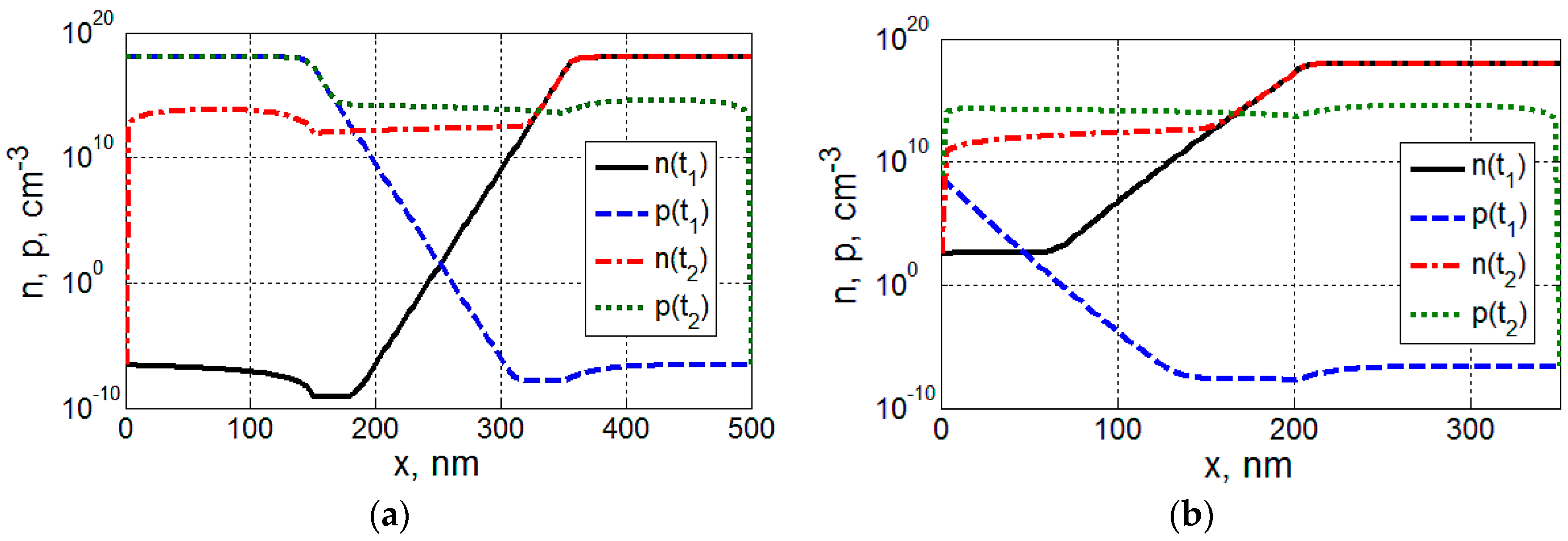
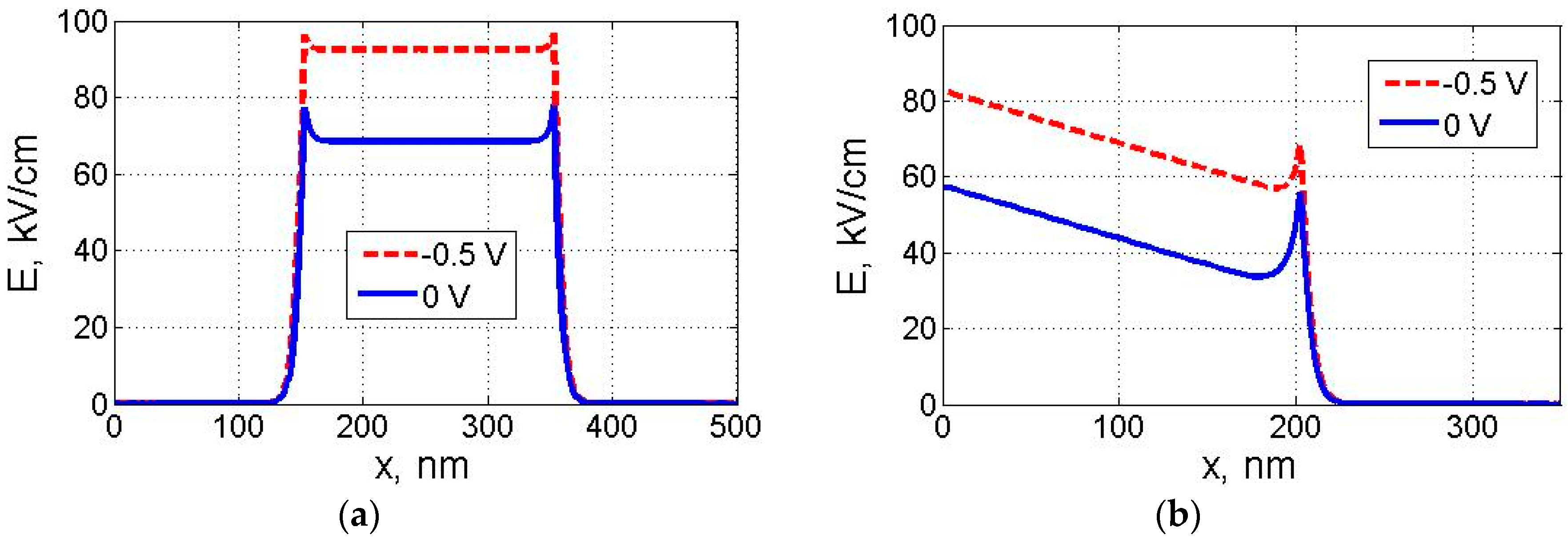
Figure 4 and Figure 5 show the distributions of carrier concentrations and the absolute values of the electric field intensity in the photodiodes being researched. The curves are computed at the active region length of 200 nm. We have calculated these results applying the developed models and numerical simulation technique. The analysis of the curves shown in Figure 5 allows us to conclude that the aforementioned photosensitive devices are characterized by the appreciable values of built-in electric field intensity in active regions. This results in significant influence on the values of carrier mobilities.
Figure 6 shows the distributions of the current density flowing through the GaAs p-i-n photodiode during the supply and illumination transient processes. To compute these curves, we have applied Slotboom Equations (37) and (38). The simulation results indicate the adequacy of the proposed technique of the current density calculation.
The results demonstrate the equality of current densities at the ohmic contacts of devices. This means the fulfillment of the principle of charge conservation. The irregularity of the coordinate distribution of the current density is a consequence of the non-equilibrium carrier generation and recombination processes taking place in the photodetector structure during the transients. It is caused by the continuity Equations (1) and (2).
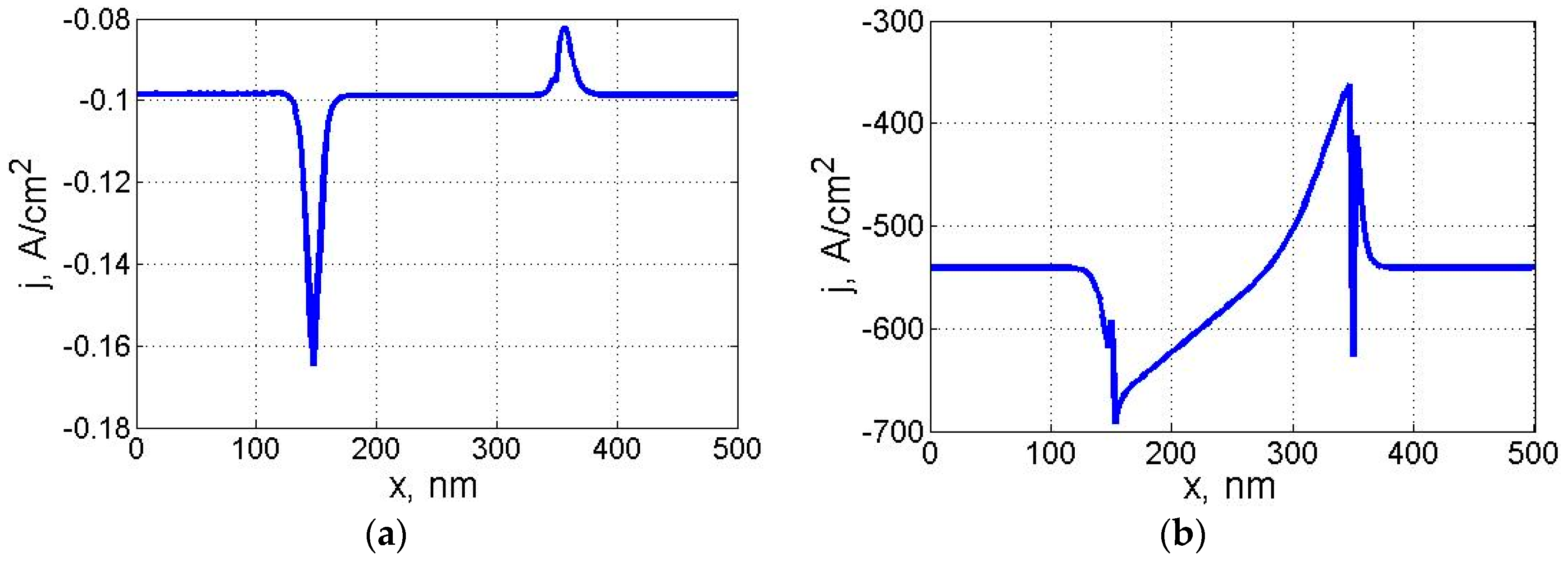
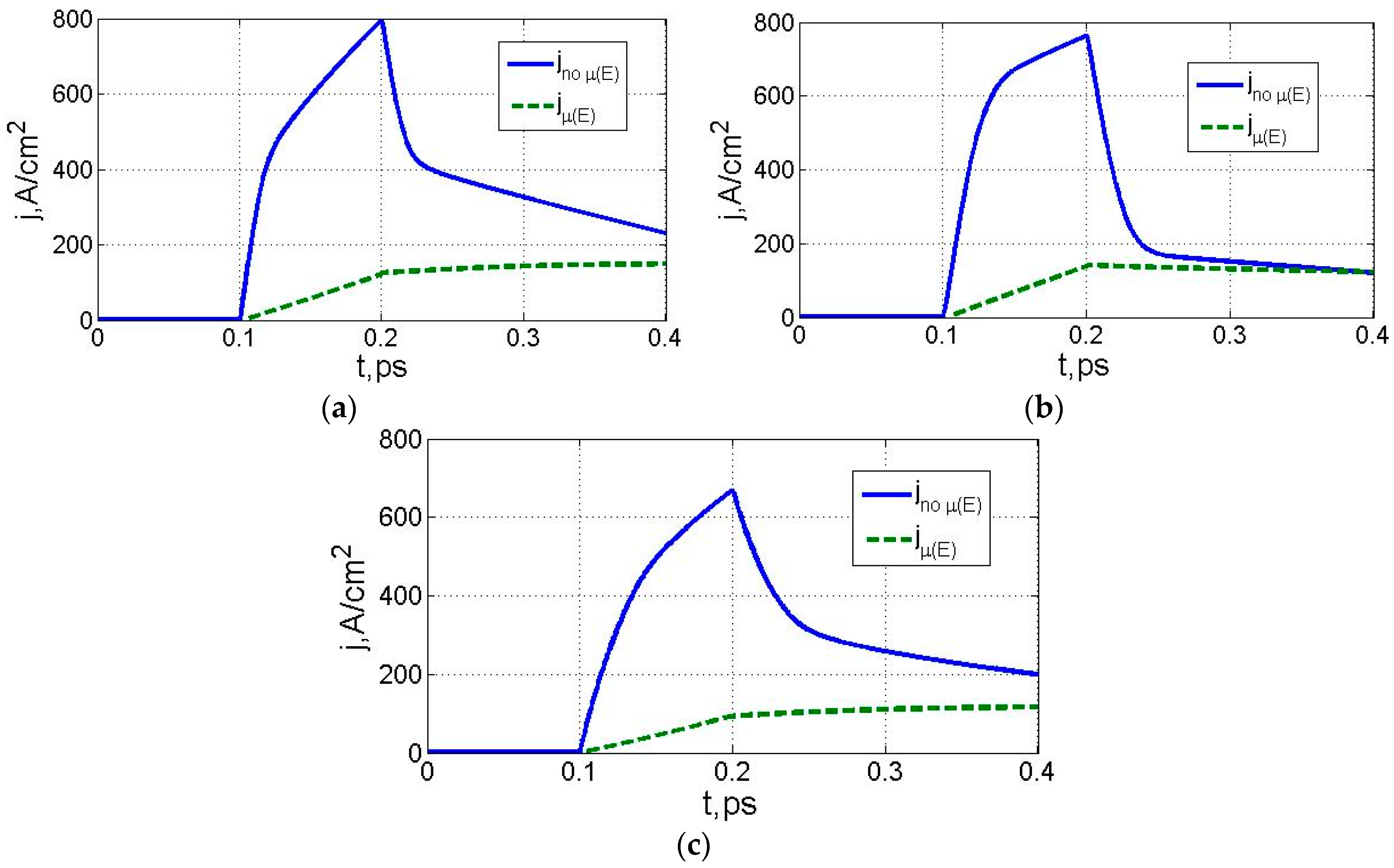
Figure 7 shows the time dependences of photocurrent density in the researched photosensitive devices. We have calculated two curves for each type of photodetectors. The first one shows the simulation results obtained with the application of low-field mobility Models (20) and (21). The second one has been computed using complex Models (20)–(26), which takes into account the effects of the electron intervalley transition and carrier drift velocity saturation in GaAs.
According to the simulation results, the influence of the effects of the electron intervalley transition and carrier drift velocity saturation on the performance of on-chip photodetectors is significantly negative. The benchmark analysis has not identified the principal difference between the performances of the GaAs p-i-n structure and Schottky-barrier photodiodes with n and p near-contact regions. Taking into account the dependence of the carrier drift velocity on the electric field intensity, it is concluded that the response times of these devices are insufficient for the adequate detection of subpicosecond laser pulses.
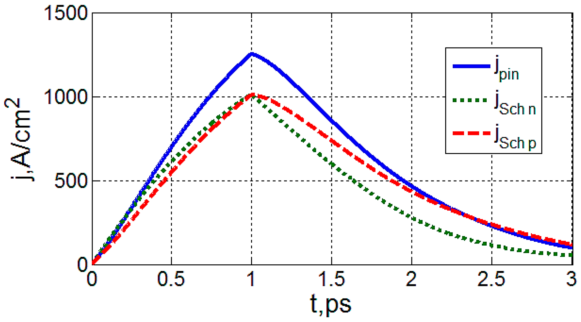
Figure 8 shows the photocurrent simulation results calculated for the optical pulses with the duration of 1 ps. The total simulation time was 3 ps. We have computed these curves taking into account the dependence of carrier mobility on the electric field intensity in photodetector structure. According to the represented results, GaAs p-i-n and Schottky-barrier photodiodes provide the adequate detection of the laser pulses with a duration of 1 ps and above.
According to the simulation results, the back edge of the photocurrent pulse is longer than the leading one. This effect is caused by the lag of photogenerated carrier recombination. In this research, we have attempted to provide the equality of photocurrent pulse edges by means of the reduction of charge carrier average lifetime at the increase in the trap concentration and the deepening of the trap energy levels. We have found out the following. Photocurrent pulse edges have approximately equal duration in the case of the enormous trap density close to the limit concentration of impurities in GaAs. That is why this method seems to be not promising within the problem being considered.
Figure 9 shows the dependence of photocurrent density on time for the GaAs p-i-n photodiode being illuminated by the modulated optical signal. The volume power density of the optical radiation varies sinusoidally. The frequency of the sine ranges from 300 GHz to 3 THz linearly. The constant component of the optical signal corresponds to the incident radiation power of 0.8 mW.
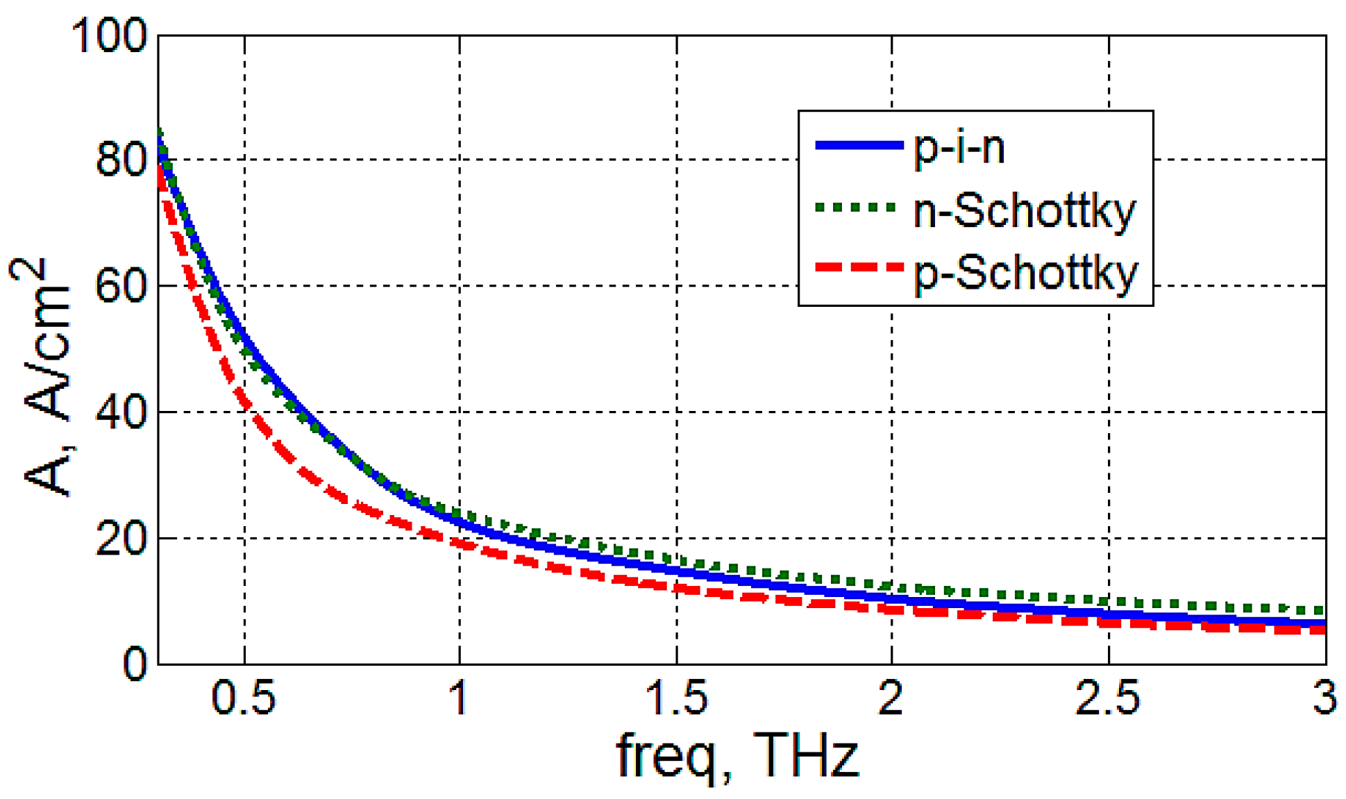
The amplitude-frequency characteristics calculated for different types of GaAs on-chip photodetectors at the aforementioned frequency range are shown in Figure 10. We can divide these curves into two regions. The first one is characterized by a steep slope of curves. It corresponds to the frequencies from 300 to about 700 GHz. The photosensitive devices provide the adequate detection of optical signals at such modulation frequencies. The second region corresponds to the frequencies of about 700 GHz and above. The curves have a shallow slope in this region. This means that the amplitude-frequency response is insufficient for the adequate detection of optical signals at such modulation frequencies. Different types of photodetectors have roughly similar magnitudes of amplitude-frequency response at the range being considered.
According to the obtained simulation results, the active area elongation has a negative impact on the response time of the GaAs p-i-n photodetector. We can explain this fact as follows. It is obvious that the performance of the photodiode depends on the time of photogenerated carrier drift transit through the active region of the device. We can estimate the maximal carrier transit time using the following equation:
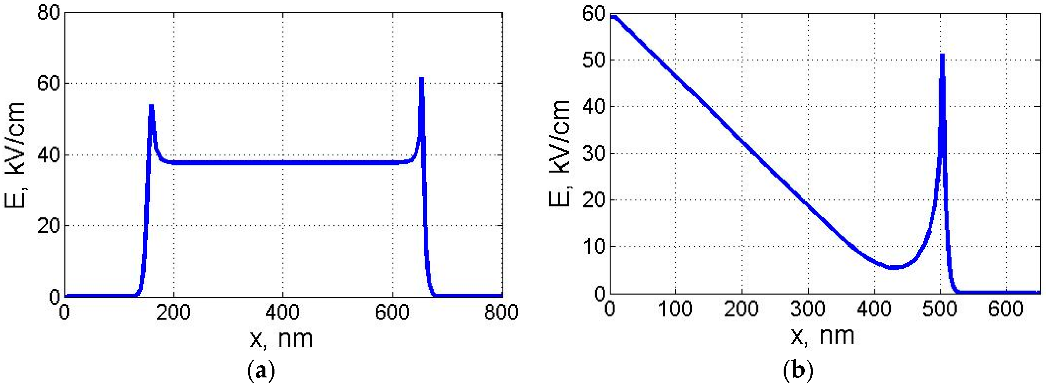
where is the length of the active region; is the average carrier drift velocity. If other conditions are equal, the increase in leads to the electric field reduction in the photodetector. According to Figure 2c,d, this results in a certain mobility growth. The adequate values of are 500 nm and less. The electric field intensity is sufficient for the saturation of the carrier drift velocity at such a length of the active region (see Figure 11a). This means that the aforementioned electric field reduction at the active region elongation does not lead to the notable change of carrier drift velocity (see Figure 2a,b). According to Equation (40), if the carrier drift velocity is constant, the increase in the length of the active region results in the proportional growth. That is why the response time of the p-i-n photodetector with the extended active region is longer than the response time of the device with the short one.
We can reduce significantly the electric field intensity in the structure of the Schottky-barrier photodiode by means of the active region extension up to 500 nm (see Figure 11b). According to the curve and Figure 2a,c, there is a narrow area with significantly increased electron mobility and drift velocity near the intensity minimum in the active region of the device being considered. However, this effect does not result in response time improvement. This is caused by the substantial increase and the short length of the high-mobility region.
We have also researched the influence of the bias voltage value on the response time of photodetectors for on-chip optical interconnections. We have found out the following. This parameter does not affect the performance of integrated photodetectors significantly. According to Figure 5, the electric field intensity in the photodiode is sufficient for the saturation of the carrier drift velocity at the zero bias voltage. Consequently, in this case, all parameters in Equation (40) are unchanged. Thus, integrated photodiodes can efficiently operate in the short-circuit mode at the zero bias voltage without significant response time degradation. The application of such a mode will provide the high energy performance of on-chip optical interconnections.
4. Conclusions
In this paper, we propose the numerical non-stationary drift-diffusion models, simulation technique and software allowing one to research transient processes in photodetectors for on-chip optical interconnections. It should be noted that the modelling aids being considered provide the simulation of devices with different electrophysical, constructive and technological parameters. We have developed the original numerical drift-diffusion simulation technique. It is characterized by the optimal balance between the adequacy of the simulation results and the consumption of time and computational resources. We compared the technique with its counterparts. The benchmark analysis indicates the advantage of the proposed approach within the problem of photodetector simulation. It is applicable for the solution of other problems in the field of semiconductor device simulation.
In this research, we take into account the effects of electron intervalley transition and carrier drift velocity saturation in AIIIBV materials. We apply the simple analytical model for the calculation of the carrier mobility dependence on electric field intensity. We have found out the significant influence of the effects being considered on the response time of the on-chip photodetectors.
In this article, we have researched the carrier transport and accumulation processes in GaAs p-i-n and Schottky-barrier photodiodes during the detection of subpicosecond laser pulses. We have found out the following. The insufficient response time of such photosensitive devices at the detection of subpicosecond laser pulses is caused by the effects of the electron intervalley transition and carrier drift velocity saturation. This means that this characteristic is improvable by means of the reduction of the electric field intensity in the structures of photodetectors.
We did not find out any principal differences between the performance of GaAs p-i-n and Schottky-barrier photodiodes. According to the simulation results, such devices can provide the adequate detection of the laser pulses with the duration of about 1 ps and above. That is why it is necessary to develop the improved structure of the photodetector for the on-chip optical interconnections based on high-speed laser modulators.
According to the simulation results, carrier drift velocities (especially the electron one) are essential parameters determining the response time of integrated photodetectors. The development of methods aimed at the reduction of the built-in electric field in the active region is a reasonable way for photodetector improvement. The electric field intensity in the device structure should be reduced to values corresponding to the near-peak area of the electron drift velocity distribution (Figure 2a). Herewith, we should provide a small length of the active region in order to reduce the carrier transit time.
Acknowledgments
The results have been obtained using the equipment of the Shared Equipment Center and the Research and Educational Center “Nanotechnology” of the Institute of Nanotechnologies, Electronics and Electronic Equipment Engineering, Southern Federal University (Taganrog, Russia). This research is supported by the Russian Foundation for Basic Research (Grant 16-07-00018) and the Ministry of Education and Science of the Russian Federation (Project 8.797.2014K).
Author Contributions
E.R. developed the drift-diffusion models of integrated photodetectors. E.R. and I.P. designed the non-stationary drift-diffusion simulation technique and wrote the paper. I.P. developed the software, performed the computational experiments and analyzed the simulation results.
Conflicts of Interest
The authors declare no conflict of interest. The founding sponsors had no role in the design of the study; in the collection, analyses or interpretation of data; in the writing of the manuscript; nor in the decision to publish the results.
References
Ceyhan, A.; Naeemi, A. Cu interconnect limitations and opportunities for SWNT interconnects at the end of the roadmap. IEEE Trans. Electron Dev.2013, 60, 374–382. [Google Scholar] [CrossRef]
Kimerling, L.C.; Dal Negro, L.; Saini, S.; Yi, Y.; Ahh, D.; Akiyama, S.; Cannon, D.; Liu, J.; Sandland, J.G.; Sparacin, D.; et al. Monolithic silicon microphotonics. In Silicon Photonics; Pavesi, L., Lockwood, D.J., Eds.; Springer Science + Business Media: Berlin, Germany, 2004; pp. 89–120. [Google Scholar]
Chang, M.-C.F.; Socher, E.; Tam, S.-W.; Cong, J.; Reinman, G. RF Interconnects for Communications On-Chip. In Proceedings of the IEEE International Symposium on Physical Design, Portland, OR, USA, 13–16 April 2008; pp. 78–83.
Subash, S.; Kolar, J.; Chowdhury, M.H. A new spatially rearranged bundle of mixed carbon nanotubes as VLSI interconnection. IEEE Trans. Nanotechnol.2013, 12, 3–12. [Google Scholar] [CrossRef]
Naeemi, A.; Meindl, J.D. Conductance modeling for graphene nanoribbon (GNR) interconnects. IEEE Electron Device Lett.2007, 28, 428–431. [Google Scholar] [CrossRef]
Rakheja, S.; Naeemi, A. Modeling interconnects for post-CMOS devices and comparison with copper interconnects. IEEE Trans. Electron Dev.2011, 58, 1319–1328. [Google Scholar] [CrossRef]
Stucchi, M.; Cosemans, S.; van Campenhout, J.; Tokei, Z.; Beyer, G. Benchmarking On-Chip Optical Against Electrical Interconnect for High-Performance Applications. In Proceedings of the IEEE International Interconnect Technology Conference, Dresden, Germany, 8–12 May 2011; pp. 1–3.
Ohashi, K.; Nishi, K.; Shimizu, T.; Nakada, M.; Fujikata, J.; Ushida, J.; Toru, S.; Nose, K.; Mizuno, M.; Yukawa, H.; et al. On-chip optical interconnect. Proc. IEEE2009, 97, 1186–1198. [Google Scholar] [CrossRef]
Spuesens, T.; Bauwelinck, J.; Regreny, P.; van Thourhout, D. Realization of a compact optical interconnect on silicon by heterogeneous integration of III-V. IEEE Photonics Technol. Lett.2013, 25, 1332–1335. [Google Scholar] [CrossRef]
Dai, X.; Nguyen, B.-M.; Hwang, Y.; Soci, S.; Dayeh, S.A. Novel heterogeneous integration technology of III-V layers and InGaAs FinFETs to silicon. Adv. Funct. Mater.2014, 24, 4420–4426. [Google Scholar] [CrossRef]
Konoplev, B.G.; Ryndin, E.A.; Denisenko, M.A. Diffusion-drift model of the transport of charge carriers and photons in injection lasers. Tech. Phys. Lett.2015, 41, 587–590. [Google Scholar] [CrossRef]
Konoplev, B.G.; Ryndin, E.A.; Denisenko, M.A. Injection laser with a functionally integrated frequency modulator based on spatially shifted quantum wells. Tech. Phys. Lett.2013, 39, 386–389. [Google Scholar] [CrossRef]
Konoplev, B.G.; Ryndin, E.A.; Denisenko, M.A. Components of integrated microwave circuits based on complementary coupled quantum regions. Russ. Microelectron.2015, 44, 190–196. [Google Scholar] [CrossRef]
Unlu, M.S.; Onat, B.M.; Leblebici, Y. Transient simulation of heterojunction photodiodes—Part II: Analysis of resonant cavity enhanced photodetectors. J. Lightwave Technol.1995, 13, 406–415. [Google Scholar] [CrossRef]
Suzuki, G.; Konno, K.; Navarro, D.; Sadachika, N.; Mizukane, Y.; Matsushima, O.; Miura-Mattausch, M. Time-Domain-Based Modeling of Carrier Transport in Lateral p-i-n Photodiode. In Proceedings of the International Conference on Simulation of Semiconductor Processes and Devices, Tokyo, Japan, 1–3 September 2005; Taniguchi, K., Hane, M., Eds.; pp. 107–110.
Goswami, S.; Davis, L.; Bhattacharya, P.K. Temporal response of photodiodes with GaAs/AlxGa1-xAs (0.1 ≤ x ≤ 0.3) multiquantum well absorption regions. J. Appl. Phys.1992, 72, 4888–4892. [Google Scholar] [CrossRef]
Lundstrom, M. Drift-diffusion and Computational Electronics—Still Going Strong after 40 Years! In Proceedings of the International Conference on Simulation of Semiconductor Processes and Devices, Washington, DC, USA, 9–11 September 2015; pp. 1–3.
Pisarenko, I.; Ryndin, E.; Denisenko, M. Diffusion-drift model of injection lasers with double heterostructure. J. Phys.: Conf. Ser.2015, 586, 012015. [Google Scholar] [CrossRef]
Nanz, G. A Critical Study of Boundary Conditions in Device Simulation. In Proceedings of the 4th International Conference on Simulation of Semiconductor Devices and Processes, Zurich, Switzerland, 12–14 September 1991; Fichtner, W., Aemmer, D., Eds.; Hartung-Gorre: Konstanz, Germany, 1991; pp. 321–328. [Google Scholar]
Gummel, H.K. A self-consistent iterative scheme for one-dimensional steady-state transistor calculations. IEEE Trans. Electron Devices1964, 11, 455–465. [Google Scholar] [CrossRef]
Slotboom, J.W. Computer-aided two-dimensional analysis of bipolar transistors. IEEE Trans. Electron Devices1973, 20, 669–679. [Google Scholar] [CrossRef]
Palankovski, V.; Quay, R. Analysis and Simulation of Heterostructure Devices; Springer: Vienna, Austria, 2004. [Google Scholar]
Ünlü, M.S.; Strite, S. Resonant cavity enhanced photonic devices. J. Appl. Phys.1995, 78, 607–639. [Google Scholar] [CrossRef]
Saleh, B.E.A.; Teich, M.C. Fundamentals of Photonics, 2nd ed.; Wiley-Interscience: Hoboken, NJ, USA, 2007. [Google Scholar]
Mnatsakanov, T.T.; Levinshtein, M.E.; Pomortseva, L.I.; Yurkov, S.N. Universal analytical approximation of the carrier mobility in semiconductors within a wide range of temperatures for a variety of doping densities. Semiconductors2004, 38, 56–60. [Google Scholar] [CrossRef]
Yngvesson, S. Microwave Semiconductor Devices; Springer Science + Business Media: New York, NY, USA, 1991. [Google Scholar]
Smith, P.M.; Inoue, M.; Frey, J. Electron velocity in Si and GaAs at very high electric fields. Appl. Phys. Lett.1980, 37, 797–798. [Google Scholar] [CrossRef]
Barry, D.M.; Platt, S.P.; Snowden, C.M.; Howes, M.J.; Miles, R.E. Physical modelling of GaAs photodetectors. In Proceedings of the 3rd International Conference on Simulation of Semiconductor Devices and Processes, Bologna, Italy, 26–28 September 1988; Baccarani, G., Rudan, M., Eds.; pp. 31–42.
Požela, J.; Reklaitis, A. Electron transport properties in GaAs at high electric fields. Solid-State Electron.1980, 23, 927–933. [Google Scholar] [CrossRef]
Dalal, V.L. Temperature dependence of hole velocity in p-GaAs. J. Appl. Phys.1971, 42, 2864–2867. [Google Scholar] [CrossRef]
Samarskii, A.A. The Theory of Difference Schemes; Marcel Dekker: New York, NY, USA; Basel, Switzerland, 2001. [Google Scholar]
Fletcher, S.A.J. Computational Techniques for Fluid Dynamics 1. Fundamental and General Techniques, 2nd ed.; Springer-Verlag Berlin Heidelberg: Berlin, Germany, 1998. [Google Scholar]
Figure 1.
The structure chart of typical on-chip optical interconnection.
Figure 1.
The structure chart of typical on-chip optical interconnection.
Figure 2.
The dependences of average electron (a) and hole drift velocities (b) an the electron (c) and hole mobilities (d) on the electric field intensity in GaAs. The curves are calculated at different impurity concentrations applying Models (20)–(26) and the experimental data given in the paper [38].
Figure 3.
Structures of the researched photodetectors for on-chip optical interconnections: GaAs p-i-n (а) and Schottky-barrier (b) photodiodes: 1, integrated optical waveguide; 2, half reflecting mirror; 3, ohmic contacts; 4, totally reflecting mirror; 5, metal layer of Schottky contact.
Figure 3.
Structures of the researched photodetectors for on-chip optical interconnections: GaAs p-i-n (а) and Schottky-barrier (b) photodiodes: 1, integrated optical waveguide; 2, half reflecting mirror; 3, ohmic contacts; 4, totally reflecting mirror; 5, metal layer of Schottky contact.
Figure 4.
Electron (n) and hole (p) concentrations in the structures of GaAs p-i-n (a) and n-type Schottky-barrier (b) photodiodes at the instants of the leading () and back () edges of the rectangular laser pulse.
Figure 4.
Electron (n) and hole (p) concentrations in the structures of GaAs p-i-n (a) and n-type Schottky-barrier (b) photodiodes at the instants of the leading () and back () edges of the rectangular laser pulse.
Figure 5.
Spatial distributions of the electric field intensity modulus in p-i-n (a) and n-type Schottky-barrier (b) photodiodes at zero and working values of supply voltage.
Figure 5.
Spatial distributions of the electric field intensity modulus in p-i-n (a) and n-type Schottky-barrier (b) photodiodes at zero and working values of supply voltage.
Figure 6.
Spatial distributions of the current density flowing through the GaAs p-i-n photodiode during the supply (a) and illumination (b) transient processes.
Figure 6.
Spatial distributions of the current density flowing through the GaAs p-i-n photodiode during the supply (a) and illumination (b) transient processes.
Figure 7.
The dependences of photocurrent density modulus on time in GaAs p-i-n (a); n-type (b) and p-type Schottky-barrier (c) photodiodes calculated with the application of different mobility models: low-field Models (20) and (21) (); complex Models (20)–(26) (), which take into account the effects of electron intervalley transition and carrier drift velocity saturation in GaAs.
Figure 8.
The time dependences of the photocurrent density modulus calculated at the optical pulse duration of 1 ps for the GaAs p-i-n structure () and Schottky-barrier photodiodes with n () and p () near-contact regions.
Figure 8.
The time dependences of the photocurrent density modulus calculated at the optical pulse duration of 1 ps for the GaAs p-i-n structure () and Schottky-barrier photodiodes with n () and p () near-contact regions.
Figure 9.
The dependence of photocurrent density on time computed for device being illuminated by the optical signal with sinusoidally-modulated volume density of optical power at the frequency ranging from 300 GHz to 3 THz.
Figure 9.
The dependence of photocurrent density on time computed for device being illuminated by the optical signal with sinusoidally-modulated volume density of optical power at the frequency ranging from 300 GHz to 3 THz.
Figure 10.
Amplitude-frequency characteristics of different types of GaAs photodetectors calculated at the frequency ranging from 300 GHz to 3 THz.
Figure 10.
Amplitude-frequency characteristics of different types of GaAs photodetectors calculated at the frequency ranging from 300 GHz to 3 THz.
Figure 11.
The coordinate distributions of electric field intensity modulus in the GaAs p-i-n structure (a) and Schottky-barrier photodiode with the n-type near-contact region (b) at the active region length of 500 nm.
Figure 11.
The coordinate distributions of electric field intensity modulus in the GaAs p-i-n structure (a) and Schottky-barrier photodiode with the n-type near-contact region (b) at the active region length of 500 nm.
Table 1.
Impurity concentrations in the regions of photodetectors.
Table 1.
Impurity concentrations in the regions of photodetectors.
Pisarenko, I.; Ryndin, E.
Numerical Drift-Diffusion Simulation of GaAs p-i-n and Schottky-Barrier Photodiodes for High-Speed AIIIBV On-Chip Optical Interconnections. Electronics2016, 5, 52.
https://doi.org/10.3390/electronics5030052
AMA Style
Pisarenko I, Ryndin E.
Numerical Drift-Diffusion Simulation of GaAs p-i-n and Schottky-Barrier Photodiodes for High-Speed AIIIBV On-Chip Optical Interconnections. Electronics. 2016; 5(3):52.
https://doi.org/10.3390/electronics5030052
Chicago/Turabian Style
Pisarenko, Ivan, and Eugeny Ryndin.
2016. "Numerical Drift-Diffusion Simulation of GaAs p-i-n and Schottky-Barrier Photodiodes for High-Speed AIIIBV On-Chip Optical Interconnections" Electronics 5, no. 3: 52.
https://doi.org/10.3390/electronics5030052
APA Style
Pisarenko, I., & Ryndin, E.
(2016). Numerical Drift-Diffusion Simulation of GaAs p-i-n and Schottky-Barrier Photodiodes for High-Speed AIIIBV On-Chip Optical Interconnections. Electronics, 5(3), 52.
https://doi.org/10.3390/electronics5030052
Note that from the first issue of 2016, this journal uses article numbers instead of page numbers. See further details here.
Article Metrics
No
No
Article Access Statistics
For more information on the journal statistics, click here.
Multiple requests from the same IP address are counted as one view.
Pisarenko, I.; Ryndin, E.
Numerical Drift-Diffusion Simulation of GaAs p-i-n and Schottky-Barrier Photodiodes for High-Speed AIIIBV On-Chip Optical Interconnections. Electronics2016, 5, 52.
https://doi.org/10.3390/electronics5030052
AMA Style
Pisarenko I, Ryndin E.
Numerical Drift-Diffusion Simulation of GaAs p-i-n and Schottky-Barrier Photodiodes for High-Speed AIIIBV On-Chip Optical Interconnections. Electronics. 2016; 5(3):52.
https://doi.org/10.3390/electronics5030052
Chicago/Turabian Style
Pisarenko, Ivan, and Eugeny Ryndin.
2016. "Numerical Drift-Diffusion Simulation of GaAs p-i-n and Schottky-Barrier Photodiodes for High-Speed AIIIBV On-Chip Optical Interconnections" Electronics 5, no. 3: 52.
https://doi.org/10.3390/electronics5030052
APA Style
Pisarenko, I., & Ryndin, E.
(2016). Numerical Drift-Diffusion Simulation of GaAs p-i-n and Schottky-Barrier Photodiodes for High-Speed AIIIBV On-Chip Optical Interconnections. Electronics, 5(3), 52.
https://doi.org/10.3390/electronics5030052
Note that from the first issue of 2016, this journal uses article numbers instead of page numbers. See further details here.


