Abstract
In the age of hardware accelerators, increasing pressure is applied on computer architects and hardware engineers to improve the balance between the cost and benefits of specialized computing units, in contrast to more general-purpose architectures. The first part of this study presents the embedded Streaming Hardware Accelerator (eSAC) architecture. This architecture can reduce the idle time of specialized logic. The remainder of this paper explores the integration of an eSAC into a Central Processing Unit (CPU) core embedded inside a System-on-Chip (SoC) design, using the AXI-Stream protocol specification. The three evaluated architectures are the Tightly Coupled Streaming, Protocol Adapter FIFO, and Direct Memory Access (DMA) Streaming architectures. When comparing the tightly coupled architecture with the one including the DMA, the experiments in this paper show an almost 3× decrease in frame latency when using the DMA. Nevertheless, this comes at the price of an increase in FPGA resource utilization as follows: LUT (2.5×), LUTRAM (3×), FF (3.4×), and BRAM (1.2×). Four different test scenarios were run for the DMA architecture, showcasing the best and worst practices for data organization. The evaluation results highlight that poor data organization can lead to a more than 7× increase in latency. The CPU model was selected as the newly released MicroBlaze-V softcore processor. The designs presented herein successfully operate on a popular low-cost Field-Programmable Gate Array (FPGA) development board at 100 MHz. Block diagrams, FPGA resource utilization, and latency metrics are presented. Finally, based on the evaluation results, possible improvements are discussed.
1. Introduction
Accelerating applications by employing specialized hardware is an evergreen topic in computer architecture. The decline of Dennard Scaling and Moore’s Law started the race to find new means to build System-on-Chip (SoC) designs that satisfy the latest application requirements. One approach is to design custom computing architectures specifically developed for an application domain that offer significant performance gains for that domain [1]. In this age of hardware accelerators, increasing pressure is applied on computer architects and hardware engineers to improve the balance between the cost and benefits of specialized computing units, in contrast to more general-purpose architectures. Newly designed computing architectures must provide a comfortable level of programmability to make them accessible to software engineers. Ease of use decreases development costs and time to market. Another way of reducing costs is by leveraging an open-source Instruction Set Architecture (ISA), such as RISC-V [2]. It consists of basic instruction sets and modular extensions that explicitly support domain-specific custom extensions. A significant body of work proposes hardware accelerators and instruction set extensions for the RISC-V ISA. Application domains targeted for acceleration include digital signal processing, communication infrastructure, and information security [3]. Artificial Intelligence (AI) is an application domain that has sparked special interest from the research community, which is committed to designing various computing architectures to accelerate AI workloads [4].
This paper presents the embedded Streaming Hardware Accelerator (eSAC) and several architectural models for integrating it in an RISC-V based SoC design implemented in a minimal Field-Programmable Gate Array (FPGA) system comprising a Central Processing Unit (CPU) and Block Random Access Memory (BRAM) data memory. Block diagrams, FPGA resource utilization, and latency metrics are presented. The results and ideas for improvement are also discussed. Latency was measured by an RTL behavioral simulation and validated using a system-integrated logic analyzer (ILA) implemented on the target FPGA chip. The designs presented herein successfully operate at a clock frequency of 100 MHz.
The primary goal of this study is to explore and evaluate efficient architectural strategies for integrating a custom accelerator (eSAC) into an RISC-V-based SoC using DMA-driven data transfer. By focusing on the impact of DMA data organization and architectural coupling on latency and resource utilization, the study aims to identify design trade-offs that directly influence performance metrics in streaming applications.
To the best of the authors’ knowledge, this is the first study that evaluates Direct Memory Access (DMA) data movement performance on AXI-Stream interfaces inside an RISC-V-based SoC design using FPGA prototyping.
This paper is organized as follows. Section 2 presents relevant related work. Section 3 describes the AXI-Stream interface specification, which is the main interconnect protocol employed in the proposed architectures. Section 4 describes the eSAC architecture and the connection models. The evaluation methodology is presented in Section 5. The results and discussion are presented in Section 6. Finally, Section 7 concludes this study.
2. Related Work
In [5], the authors presented the many-accelerator architecture, a design approach in which tens or hundreds of accelerators are integrated into homogeneous multi-core systems. The main goal was to optimize the Static RAM (SRAM) memory footprint, which accounts for up to 90% of the total accelerator footprint. The authors achieved a significant reduction of up to 30% in exchange for a 2% performance penalty, while the energy consumption changed in the range of ±8%. The solution is called the Accelerator Store (AS), a scalable architectural component that manages memory sharing between accelerators. One problem identified in this study is that, in many-accelerator designs, some accelerators, at a given moment in time, are gated off, because their functionality is not momentarily needed. This helps reduce power, but the silicon becomes “dark”—i.e., it is not used, meaning it is wasted for a given amount of time of inactivity. One possible solution is the decomposition of one accelerator into multiple fine-grained accelerators, which implement more commonly used computations and algorithms and are less application-specific. This idea comes up later in this paper, under the name of “data flow chain”, in a discussion independent of this related work.
The computing paradigm of stream processing was employed in [6] in the context of a heterogeneous system comprising a host processor, shared memory, and multiple hardware kernels accelerating computationally intensive functions of the application. The authors propose a hardware–software streaming model organized in the stages of the streaming model and in the steps of the algorithm. Several steps are executed in parallel during each stage. The steps are mapped into stages, where one step can be executed by the host or kernel, usually the host handling the I/O. The workload of the system implementing the proposed architecture is in the field of image processing, namely, the Canny edge detector algorithm.
The authors of [7] present a generalized hardware accelerator for complicated functions. These functions were computed using CORDIC [8] operators.
The study in [9] introduced a full-stack methodology for integrating accelerators in a scalable manner for multi-tenant execution. The proposed methodology provides an abstraction between the user’s view of the accelerators and physical accelerator instances, similar to virtual memory systems. The authors showed an improvement in the system throughput of 2.04× for Network-on-Chip (NoC) and 1.38× for crossbar compared to prior work, with a 2.7% hardware area overhead.
In [10], the authors introduce an elastic Coarse-Grained Reconfigurable Architecture (CGRA) named Streaming Elastic CGRA (STRELA). It is a modular architecture comprising multiple elastic logic Processing Elements (PEs) that support latency-tolerant data interchanges using valid and ready signals, and FIFOs, to communicate with the neighboring PEs. The data are processed by the Functional Unit (FU) inside the PE. Although data are streamed between the PEs, the AXI-Stream specification [11] is not mentioned in this work. The authors connected the accelerator to an RISC-V core by using the X-HEEP open-source platform [12].
A DMA evaluation is carried out in [13], where the authors present a study on the DMA transfer latency. The study focuses on the Peripheral Component Interconnect Express (PCIe) interface between an FPGA and a host running a Linux operating system distribution. The differences between [13] and the present study lie in the system architecture, in the Xilinx DMA Intellectual Property (IP) used, and the type of memory on the FPGA platform.
The paper cited in [14] presents a comprehensive review of current hardware solutions designed to accelerate neural network computations. The methodology involves analyzing and comparing different hardware platforms—such as FPGAs, ASICs, GPUs, and CPUs—used for accelerating various types of neural networks. The study highlights major design challenges such as power consumption, area, speed, throughput, and resource efficiency. Through an extensive survey of recent implementations and experimental results, the authors identify trade-offs in architecture choices, dataflows, memory hierarchy, and precision.
3. Overview of AXI-Stream
The Advanced eXtensible Interface (AXI) [15] is an on-chip communication bus protocol, part of the Advanced Microcontroller Bus Architecture (AMBA) specification. It is being developed and maintained by ARM. The AMBA is a set that includes a variety of communication protocol specifications, each suited for a specific purpose. In this study, the protocol of interest is generically named AXI-Stream [11]. This is a point-to-point protocol, connecting a single Transmitter to a single Receiver.
Data transfer in the AXI-Stream specification is conceptually similar to the burst type of transaction described by the AXI Protocol specification, but different in its being a lightweight version thereof.
The handshake mechanism requires only two single-bit signals: TVALID and TREADY. The Transmitter controls TVALID, whereas the Receiver drives the complementary TREADY. There are three possible scenarios of successful handshaking [11]. Part A in Figure 1 shows the case where the Transmitter is ready for a new transfer before the Receiver is. The Transmitter prepares the INFORMATION signals (TDATA, TUSER, and other sideband signals) and asserts the TVALID signal. Once the Receiver is ready to latch incoming data, it asserts the TREADY signal and the transfer occurs in the same clock cycle; Part B in Figure 1 presents the case where the Receiver asserts the TREADY signal and is ready for a new transfer before the Transmitter. Once the Transmitter is ready to output data, it drives the TVALID signal high, and the transfer occurs in the same clock cycle; Part C in Figure 1 shows three consecutive transfers when both the Transmitter and the Receiver are ready for three consecutive clock cycles.
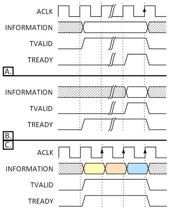
Figure 1.
AXI-Stream successful handshaking scenarios. (A) Transmitter before Receiver. (B) Receiver before Transmitter. (C) Transmitter and Receiver ready for three consecutive cycles.
Full-duplex communication is achieved by simply duplicating all protocol-specific signal lines and making both sides output the TVALID signal and input the TREADY signal, as shown in Figure 2.
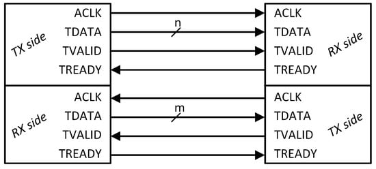
Figure 2.
AXI-Stream full duplex communication using the minimal set of standard signals. The letters n and m are placeholders for the width of the bus.
The first issue of [11] defines the AXI4-Stream protocol, whereas the latest issue introduces the AXI5-Stream protocol. This extends the first version with features of wake-up signaling and interface protection using parity bits. AXI5-Stream is not yet available as a library component in AMD Vivado. For this reason, the work presented in this paper uses the AXI4-Stream protocol specification. Future upgrading to AXI5-Stream should be a straightforward process. This requires the implementation of clock gating functionality, whereas interface protection is achieved by the simple logic of parity bit computation and validation.
Although it is a point-to-point protocol, connectivity between multiple AXI-Stream components can be achieved using an interconnected network block (conceptually similar to an AXI Crossbar). An interconnection would enable the exchange of multiple data streams between multiple transmitter interfaces and multiple receiver interfaces, respectively, based on routing information. The routing information can be stored in the standard interface signals named TDEST (destination) and TID (identifier). The standard only hints about how the routing should be implemented, exemplifying that TDEST could represent the first destination stream channel, while TID could hold the second destination channel. Nevertheless, the TUSER signal could be used to improve the routing scheme.
AXI-Stream allows for a custom transfer width that can be any number of bits, though it is recommended that this number be a power of 2, ranging from a single byte up to 128 bytes. These requirements must be maintained during the design phase. At runtime, dynamically changing the transfer width is possible using the signals named TSTRB and TKEEP. The former is the byte qualifier that indicates whether the content of the associated byte of TDATA is processed as a data byte or a position byte. The latter is the byte qualifier that indicates whether the content of the associated byte of TDATA is processed as part of the data stream. These two signals allow for flexible transfer types, where each byte can be a data byte, a position byte, or a null byte [11].
A hardware accelerator can leverage the high bandwidth of an AXI-Stream interface to receive multiple data inputs in parallel. This enables the parallel processing of data. For example, consider a hardware CORDIC [8] module computing only the atan2(imag, real) function, where the imaginary and real parts are 16-bit fixed-point inputs. To accelerate the computation for an entire array of inputs, four CORDIC modules can be employed to compute the four results in parallel. The communication interface for this accelerator, comprising four CORDIC modules, can implement the AXI-Stream specification, assigning a data width of (16-bit × 2) × 4 = 16 bytes, where each 4 bytes are processed in parallel, as shown in Figure 3.
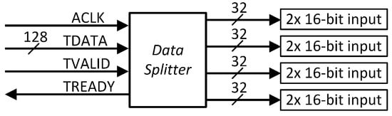
Figure 3.
AXI-Stream data splitting between four parallel computing units.
AXI transactions use a standard synchronization method based on ready/valid handshakes, which manage each data transfer on any channel. In this study, FIFO buffers are also used as an additional synchronization mechanism to support ongoing transactions. While Clock Domain Crossing (CDC) techniques are typically required to synchronize signals between different clock domains, they are not used in the current study, as all components operate within a single clock domain.
4. Proposed System Architectures
In this study, an embedded streaming hardware accelerator (eSAC) is defined as a set of Processing Elements (PEs) organized in a certain topology. A PE is a digital hardware block that performs a specific computation in a streaming, pipelined manner. A PE could be anything from a simple adder to an instance of the CORDIC [8]—or, for example, it could involve implementing a Finite Impulse Response (FIR) filter, complex transforms (Fourier, Wavelet, to name just a few), or processing stages thereof. Multiple PEs can be connected in series or in parallel to increase the versatility of the eSAC. Such a generic topology is depicted in Figure 4, where the PEs are organized in PE chains. A PE chain is represented by a series connection of PEs. For example, the first PE chain is composed of the PEs with ids 11, 12, and so forth, being the id of the last PE in chain number 1. For a more general definition, let n be the number of PE chains. Let x be an integer in the range of 1 to n. Let represent the number of PEs in the PE chain. Let y be an integer in the range of 1 to . Having defined these, let designate the PE in the chain.
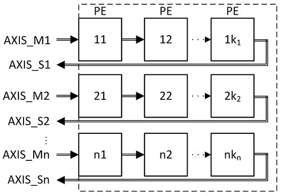
Figure 4.
The eSAC architecture as an array of arrays of PEs. The input/output to/from a chain of PEs conforms to the AXI-Stream protocol specification.
This generic architecture offers the system designer flexibility to organize the required PEs in multiple ways. Let a and b be integers in the range of 1 to n; then, it is allowed to have , which means that the PE chain number a can have a different number of PEs than the PE chain number b. For this reason, the architecture can be seen as an array of arrays, and not a matrix. Routing data between PE chains would enable composability of the computations. A data flow chain represents data flowing through two or more PE chains. A data flow chain can be achieved through the co-design of software and hardware logic. Complex algorithms can be represented as a PE chain or as a data flow chain, depending on the chosen PEs and their topology.
A PE chain inputs and outputs data through a full duplex AXI-Stream interface, where, in Figure 4, AXIS_M1 represents the input for PE chain number 1, and AXIS_S1 represents the output interface. The implementation of optional signals is the decision of the system designer. Similarly, the communication interface between one PE and the next in the chain can be the full AXI-Stream protocol specification, or just a subset thereof. This depends on the desired flexibility and reusability of the complexity constraints and the application requirements.
The following sections describe different approaches for connecting an eSAC to a CPU core. From a communication protocol perspective, this study only presents the AXI and AXI-Stream approaches. Other possibilities include, for example, the recent CV-X-IF specification [16] maintained by the OpenHW Group.
4.1. Tightly Coupled Streaming
A CPU supporting a tightly coupled AXI-Stream interface is an approach that presents itself with some trade-offs, as will be explained later. A block diagram of this architecture is shown in Figure 5. In the hardware design phase, one benefit of this architecture is represented by the lower resource utilization when incorporating the stream interface directly into the core and not requiring a protocol converter from AXI to AXI-Stream. Further reduction can be achieved by avoiding an interconnect component when connecting multiple PEs. But this may hinder other aspects of the design, such as making the CPU responsible and busy with data routing for every 32-bit of data (provided the CPU registers are 32-bit wide). For this reason, creating and maintaining data flow chains is not feasible, as every bit of data has to be moved through the CPU registers and the core must act as an AXI-Stream interconnect.
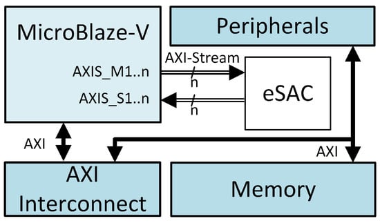
Figure 5.
Tightly coupled architecture, where MicroBlaze-V connects to hardware accelerator using AXI-Stream protocol specification.
4.2. Protocol Adapter FIFO
This architecture variant is presented in Figure 6, where the Protocol Adapter provides an AXI interface with an input FIFO (TX FIFO) and output FIFO (RX FIFO). Also present is a full-duplex AXI-Stream interface. The CPU feeds the internal TX FIFO with data and reads incoming packets from the RX FIFO. The AXI interface can be connected to the AXI Interconnect (variant 1 in Figure 6, with blue). In contrast to the tightly coupled streaming architecture, core reconfiguring is avoided during design phase, as additional PEs would simply connect to the AXI-Stream interconnect. Nevertheless, provided the core is configured with an extra AXI data port, the Protocol Adapter can be connected directly to the core (variant 2 in Figure 6, with red), as in the previous presented architecture. This alternative avoids the latency introduced by the traffic on the AXI, while also promoting the flexibility of modifying the internal topology of the eSAC. One possible drawback is the restricted access to the embedded hardware accelerator, other peripherals being unable to access it directly.
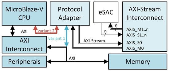
Figure 6.
Protocol Adapter architecture. The Protocol Adapter block incorporates one FIFO for incoming data on the AXI-Stream interface, and one FIFO for the outgoing data.
4.3. Direct Memory Access Streaming
Although this last system architecture model is similar to the previous one (in that the connection between the CPU and the embedded hardware accelerator is through an AXI to AXI-Stream protocol converter), the difference lies in the presence of a DMA controller. A block diagram of this architecture model is presented in Figure 7. Intuitively, this approach should provide the best trade-off between resource utilization and performance, upgradeability, and programmability. This architecture provides the lowest CPU utilization, because the DMA operates independently on data movement between the memory and the eSAC. The CPU should only enable the Scatter Gather (SG) mechanism, setup the buffer descriptors (BDs), and the chains of BDs. Achieving best performance on this architecture requires hardware–software codesign, mapping the computing requirements on the internal topology of the eSAC and aligning the data flow chains with the BD chains.
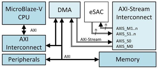
Figure 7.
Direct Memory Access Streaming architecture.
5. Architecture Evaluation Methodology
Given the interest of the industry and academic community in exploiting the RISC-V ISA, in this study, the CPU controlling the eSAC is the MicroBlaze-V soft-core processor from AMD [17]. Since the end of May 2024, release 2024.1 of the Vitis Integrated Software Platform has made the platform readily available in AMD’s Vivado Design Suite, facilitating quick system integration. The MicroBlaze-V soft-core processor is a reduced-instruction-set computer (RISC) optimized for implementation in AMD FPGA chips. It is highly configurable, allowing the system integrator to select the specific features required by the design. The base fixed feature set implements the RISC-V RV32I Base Integer Instruction Set and the machine-level ISA [2]. The MicroBlaze-V core IP also supports a tightly coupled AXI-Stream interface. For the designs presented in this paper, the instruction memory and data memory are accessible by the CPU through the Local Memory Bus (LMB) protocol defined by Xilinx (not shown in the figures). The size thereof was 32 KB each. A 32 KB BRAM component was also added in order to model the more common embedded microcontroller architecture comprising an on-chip SRAM connected to the main data bus (shown in the figures as ‘Memory’).
The software was built and debugged using the AMD Vitis 2024.1. Hardware was modeled in AMD Vivado 2024.1 and implemented on a Digilent Nexys A7-100T FPGA board. Latency reports were extracted by including the integrated logic analyzer (ILA) provided by Xilinx [18] and running the software on the target FPGA chip [19]. The latency metrics of the tightly coupled streaming and the Protocol Adapter FIFO architectures were each cross-validated by running the software on the RTL simulation [20]. The RTL simulation proved impractical for evaluating the DMA Streaming architecture, given the complexity of the hardware and software.
In the experiments presented in this study, an eSAC with only one input/output (IO) interface was used. The eSAC is modeled from the perspective of the input-to-output latency. This latency represents the number of clock cycles that elapse from the first input to the first output. In practice, data flows through the eSAC in a pipelined manner. For this reason, the modeled eSAC has an initial latency equivalent to the pipeline latency, after which it achieves a throughput of one transfer per clock cycle. For the experiments presented next, this pipeline latency was 44 cycles. This includes the input FIFO and output FIFO of the IO interface. Each FIFO is 32-bit wide (equal to the width of TDATA), and 512 words deep. The FIFOs were never driven full during the experiments. BRAM was used for FIFO implementation. The access latency of the BRAM data memory was set to one clock cycle.
No peripherals were modeled in the design. The Protocol Adapter block was modeled using the Xilinx IP presented in [21]. The DMA eployed is the Xilinx IP described in [22].
Each DMA test scenario is described by a particular data organization tailored to highlight the extent of the data organization’s impact on the overall latency. Generally, data are mapped with respect to the AXI-Stream protocol specification, and the DMA software interface functions as follows: a frame contains one or more packets, a packet contains one or more transfers, a packet is described by one or more BDs, and a BD describes an AXI-Stream data beat (Stream Beat) and contains the address pointing to an array of data, whereas an array represents one or more consecutive data words. Responsible for the data organization is the user of the hardware, namely, the software or firmware writer.
The BDs are stored sequentially in the data BRAM. Each BD points to one data buffer. The data buffers are also sequentially stored in the BRAM in the same order as the BDs, although this is not mandatory. The transferred data described by a BD are called a transaction. In this sense, a transaction comprises one or more consecutive transfers.
Four test scenarios were used to analyze the DMA performance. Data organization is the variable that differentiates one test case from another. Each test scenario comprised a total of 12 unique transfers, each transfer representing a 32-bit data movement from the data BRAM, through the Memory-mapped to Stream (MM2S) interface of the DMA (i.e., AXI to AXI-Stream), into the input FIFO of the eSAC. The result is stored in the output FIFO of the eSAC, which is then written in BRAM by the S2MM (Stream to Memory-mapped) interface of the DMA; see the data flow sequence diagram in Figure 8 for a visual representation. The M2SS is also named the transmission (TX), or Manager (M), channel of the DMA’s AXI-Stream interface. The S2MM is the reception (RX), or Subordinate (S), channel of the DMA’s AXI-Stream interface.
The first scenario is called 1P1BD (one packet, one buffer descriptor), which means that all data (12 transfers, each of 32-bit width) are contained inside the single buffer descriptor of a single packet of a single frame. This is depicted in part A in Figure 9.
The second scenario still organizes data inside one packet, but the packet contains multiple buffer descriptors, a total of twelve, one for each transfer. In this regard, this scenario is called 1P12BD and is shown in part B in Figure 9.
The third scenario—nPmBD-chaotic with n = 4 and m = 12—simulates a chaotic organization of data, where there are a total of 4 packets (n = 4) each containing a variable number of BDs (totalling 12 BDs, m = 12), where each BD contains a variable number of transfers, and the data address field is non-continuous between adjacent BDs. See part C in Figure 9 for a visual representation of the data organization and the first three columns of Table 1 for a tabular representation. The rationale behind this organization is to cover all possible combination types of the number of transfers per BD and the number of BDs per packet. This led to a total of 12 transfers, organized as follows: Packet #0 has three BDs (#0, #6, #2), with BD #0 pointing to two words, BD #6 pointing to one word, and BD #2 pointing to three words (3BD2W1W3W); Packet #1 has one BD (#5) pointing to three words (1BD3W); Packet #2 has one BD (#4) pointing to one word (1BD1W); and Packet #3 has two BDs (#3, #1) each pointing to one word (2BD1W1W). Packet order shuffling inside the frame was applied to further increase the irregularity of data organization.
A fourth scenario—nPmBD-ordered with n = 4 and m = 12—proposes ordered (continuous) data access to the memory, but the data are still scattered (fragmented) into multiple BDs (part D in Figure 9)—similar to the previous scenario, but different in that the order of the packets is not shuffled.
Data transfer occurs in the order of the packet ID. The BDs are stored in memory in the same order as they are organized inside the packet, but are processed in ascending order of their ID inside the packet.
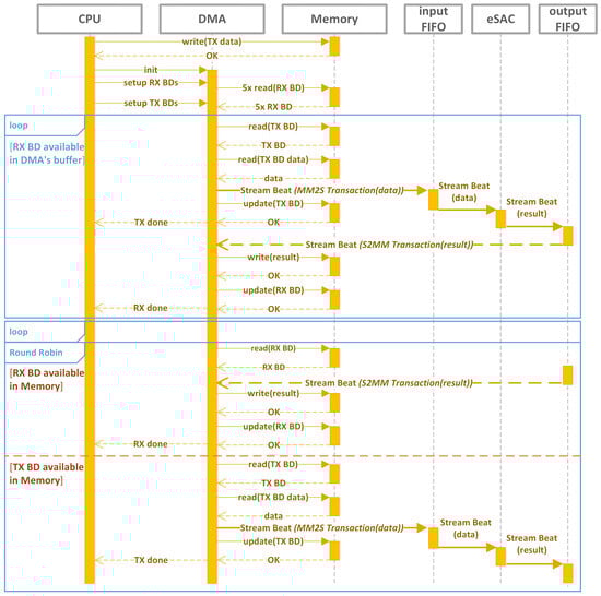
Figure 8.
Data flow sequence diagram describing how the CPU, BRAM, DMA, and the IO FIFOs of eSAC interact with each other.

Table 1.
Data organization for the nPmBD-chaotic scenario, presented in the first three rows. The last two rows contain the measured clock cycles for the operations described next. These rows describe both the chaotic and ordered scenarios. (A) Latency between the reading of the MM2S Buffer Descriptor and the start of transfer on the MM2S channel. (B) Latency between the last transfer on the MM2S channel and the start of the MM2S BD update.
| Packet ID | 0 | 0 | 0 | 1 | 2 | 3 | 3 |
| BD ID | 0 | 2 | 6 | 5 | 4 | 1 | 3 |
| Transfers per BD | 2 | 3 | 1 | 3 | 1 | 1 | 1 |
| (A) Latency | 49 | 51 | 51 | 51 | 50 | 50 | 45 |
| (B) Latency | 10 | 10 | 10 | 10 | 30 | 30 | 19 |
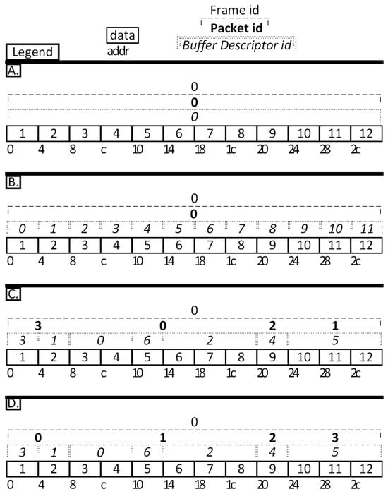
Figure 9.
(A) 1P1BD configuration. Input data organization using the constructs of frame, packet, and buffer descriptors. The data are transferred sequentially in natural order, from the lowest address to the highest address. (B) 1P12BD configuration. (C) nPmBD chaotic configuration, where n = 4 and m = 7. The data described by the BDs are transferred following the following order of BDs: 0, 6, 2, 5, 4, 3, and 1. (D) nPmBD ordered configuration, where n = 4 and m = 7. The data described by the BDs are transferred following the following order of BDs: 3, 1, 0, 6, 2, 4, and 5.
6. Results and Discussion
Resource utilization metrics are reported in Table 2, including Look-Up Table (LUT), LUTRAM, Flip-Flop (FF), and BRAM. These include the CPU core, 32KB data BRAM (connected on the AXI interface), and 32 KB instruction and data memories (on the LMB interface). These metrics do not include eSAC or the ILA. See Table 3 for the latency results, and Figure 10 for a visual representation of these measurements.
Table 2.
FPGA resource utilization for the three presented architectures (last 3 rows). “FIFOs” refers to the IO FIFOs of eSAC.
6.1. Tightly Coupled Streaming
Writing and reading from the AXI-Stream interface are performed with custom instructions. These are already implemented by the IP provider as part of the ISA. As expected, the throughput of this interface is limited by the CPU clock frequency and the 32-bit bandwidth. This means that the content from only one register can be written at a time on the interface or read from the interface. This approach significantly affects the throughput in a streaming data flow architecture. Moreover, CPU utilization would be largely capitalized by the loading and storing of data from and to the CPU registers, leading to the CPU’s role as a load–store unit.
Connecting the eSAC directly to the core would imply that the core be totally responsible for internally routing the packets between PE chains, exclusively through software. In other words, the versatility of the eSAC could be enhanced by connecting it (i.e., all PE chains) to an AXI-Stream Interconnect block. This would allow the output from one PE chain to be routed to the input of another PE chain. Routing would enable the composability of computations. This composability is the basis for implementing complex algorithms as a resource-aware approach.
The AXI-Stream interface of MicroBlaze-V is, however, limited in terms of protocol signals. The only other signals present are the handshake signals TVALID and TREADY, and the end of the packet indicator signal TLAST. Therefore, flexibility and performance are limited when the core is interfaced with an eSAC. If the core’s AXI-Stream interface has no sideband information for routing purposes, a connection with an AXI-Stream Interconnect block is impossible, because the Interconnect does not have the routing information.
6.2. Protocol Adapter FIFO
The Protocol Adapter model showcased the worst results. The almost 8x difference in CPU write latency is because of the overhead introduced by the control transactions from the CPU to the FIFO. These include requests to determine whether it can accept new data or output new results, and set the number of transfers to be output on the MM2S interface. Similar to the tightly coupled architecture, the CPU must transmit the entire frame before it can begin receiving the incoming frame. The CPU utilization was 100% focused on data movement. This type of scenario is seldom feasible in practice. CPU silicon is inefficiently utilized if the functionality of the CPU is reduced to that of a load–store unit. In this regard, the two generic main tasks of the CPU, namely, control and data processing, cannot occur in parallel in these two architectures, in contrast to the DMA architecture.
6.3. Direct Memory Access Streaming
The 1P1BD data organization yielded a 65% reduction in total latency relative to the tightly coupled model. This percentage could have been even higher if the DMA had not been required to stall waiting for eSAC to start outputting results. This scenario also achieves a minimum number of clock cycles per transfer.
From the user’s perspective, the 1P12BD scenario achieves the same functionality as the 1P1BD scenario, though with greater latency. This is correlated with the fact that each additional BD increases the communication latency by increasing the number of AXI transactions on the SG interface for reading the BD and updating it. This explains why using multiple frames or packets for data organization does not directly affect the communication latency. In this sense, having one packet whose data are described by two BDs achieves the same latency as having two packets each described by a single BD.
6.3.1. 1P1BD
This data organization achieved the best results, because there was only one BD describing the frame. For the MM2S interface, only two transactions are necessary on the SG interface: one for reading the MM2S BD and one for updating it after a successful frame transmission. The same applies to the S2MM interface: one read transaction for the S2MM BD and one write for updating it after successful frame reception. Figure 11 presents the order and the latency of the steps involved in the process of one AXI4-Stream frame transmission and reception. DMA_AXIS_SG represents the SG interface of the DMA IP. The AXI data interface is shown below in the figure. The DMA_MM2S (TX) and DMA_S2MM (RX) lines represent the transmission and reception interfaces of the DMA IP, respectively.
6.3.2. 1P12BD
Although data ordering is identical to that in the 1P1BD scenario, employing a BD for each transfer dramatically increases the latency of the frame transfer. The only difference between these two scenarios was that the data were fragmented into multiple BDs. In other words, this scenario simulates a user organizing the data in such a way that each BD points immediately next to the pointing location of the previous BD. This test case, for example, is a scenario where the user just wants to feed the AXI-Stream interface with 12 32-bit words (i.e., 12 variables) that were carefully placed in memory one next to another in order to leverage the Burst transaction of the AXI specification.
The 1P12BD scenario highlights the importance of data organization, as employing the highest number of BDs resulted in the highest latency compared with the other scenarios run on the DMA architecture. This leads to the conclusion that for the evaluated DMA IP, this detail of continuous data ordering is transparent, making this a possible improvement point. Another improvement could further abstract the DMA functionality and relieve the user (the software engineer) of the burden of knowing the details and intricacies of the hardware required to achieve a better latency.
6.3.3. nPmBD-Chaotic
The number of clock cycles starting from the BD read operation and the start of the corresponding data beat on the AXI-Stream was found to vary between 45 and 51 cycles, as shown in Figure 12 and as listed in column (A) of Table 1. The number of cycles is affected by other AXI transactions keeping the memory busy, forcing the SG interface to wait for a free slot to read the BD. This also occurs for the update of the BD after the transfer is completed (see column (B) of Table 1). The three-fold difference between BDs number 0 to 3 and BDs number 4 and 5 is explained by the update of the S2MM BD after successful transfer on the S2MM interface. This update operation consists of an AXI write transaction on the SG interface by the DMA to the BRAM memory where the BD is stored. This update was performed over 15 cycles for BDs number 4 and 5. For BD number 6, the write BD transaction was completed in seven cycles.
This increase in latency from 10 to 30 is explained by the fact that the DMA halts the MM2S interface and prioritizes the update of S2MM BDs to make received data available for the application. After the first five BD readings for MM2S, the DMA IP alternates reading and updating for the two interfaces. In other words, it alternates the reading of an MM2S BD with a reading of an S2MM BD and an update of an MM2S BD with an update of an S2MM BD. This impacts the latency between consecutive transactions on the MM2S interface, as shown in the bottom part B in Figure 12.
6.3.4. nPmBD-Ordered
This scenario is similar to the 1P12BD scenario; however, the data are further fragmented into multiple packets. As in the 1P12BD scenario, the fact that the data to be sent reside in the memory as a continuous block is neglected by the DMA. Thus, the system behaves exactly as it does in the nPmBD-chaotic scenario. It did not show any sensitivity to the fact that the address and length fields of the BDs formed a continuous memory space. The same improvement opportunity is highlighted here as in the 1P12BD scenario: the DMA could leverage this favorable placement of ordered data to benefit from the burst capabilities of the AXI interface, just as it did in the 1P1BD case.
Table 3.
See Figure 10 for a visual representation of these measurements. (A) Total latency for a complete frame transaction on the TX interface. For the non-DMA architectures, a TX frame transaction starts with reading the first data word from BRAM. It ends with the write of the last data word in the input FIFO of the PE. For the DMA architecture, a TX frame transaction starts with reading the first TX BD of the first packet from BRAM. It ends with acknowledgment of the write (update) of the last TX BD of the last packet. (B) Number of clock cycles for a complete frame transaction on the RX interface. For the non-DMA architectures, an RX frame transaction starts with reading the first data word from the output FIFO of the PE. It ends with the write of the last data word to BRAM. For the DMA architecture, an RX frame transaction starts with reading the first RX BD from BRAM. It ends with acknowledgment of the write (update) of the last RX BD of the last packet. (C) Total latency from the start of the TX frame up until the end of the RX frame. (D) Latency of CPU reading 1 word from BRAM and writing to input FIFO. (E) Latency of CPU reading 1 word from output FIFO and writing to BRAM. (*): Excluding the latency of reading the RX BD (15 clock cycles), which was carried out while the CPU was configuring the MM2S (TX) interface. (**): Excluding the latency of 5 consecutive RX BD reads (123 clock cycles), which were carried out while the CPU was configuring the MM2S (TX) interface.
| Architecture | (A) TX Frame | (B) RX Frame | (C) Both Frames | (D) CPU Write | (E) CPU Read | Latency Per Transfer-(C)/24 |
|---|---|---|---|---|---|---|
| Tightly coupled | 253 | 231 | 505 | 23 | 21 | 21 |
| MM2S Adapter | 1992 | 1221 | 3286 | 163-184 | 86 | 137 |
| DMA—1P1BD | 73 | 86 (*) | 175 (*) | - | - | 7.3 |
| DMA—1P12BD | 543 | 551 (**) | 644 (**) | - | - | 26.8 |
| DMA—nPmBD | 283 | 297 (**) | 390 (**) | - | - | 16.3 |
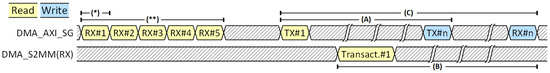
Figure 10.
Diagram on how the frame latencies have been measured in the DMA scenarios. This diagram is coupled with Table 3. For the 1P1BD scenario, there is only one BD for reception (RX BD), only one BD for transmission (TX BD), and only one transaction (in this scenario, representing the entire frame) on the TX interface and one on the RX interface, respectively. Notations (*), (**), (A), (B), and (C) are defined in Table 3.
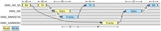
Figure 11.
1P1BD scenario. Transaction diagram on the 4 interfaces involved in the transmission and reception of an AXI-Stream frame, in the 1P1BD scenario. The numbers represent the latency measured in clock cycles. The latency of 44 cycles is the latency of the PE and its input and output FIFOs.
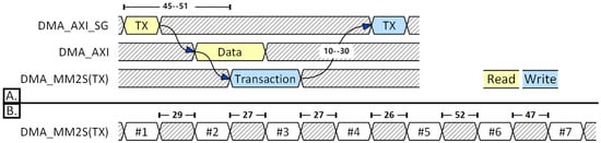
Figure 12.
nPmBD scenarios. (A) Minimum and maximum latency (45, 51) between start of TX BD read, and start of transfer on MM2S channel. Minimum and maximum latency (10, 30) between last transfer of transaction on MM2S channel, and start of TX BD update. (B). Latencies between consecutive transactions on MM2S interface.
7. Conclusions
The goal of this study—to evaluate architectural strategies for efficiently integrating a custom accelerator (eSAC) into an RISC-V-based SoC using DMA-driven data transfer—was successfully achieved through a systematic set of experiments and analyses. The study implemented and tested multiple architecture models, including tightly coupled, Protocol Adapter, and various DMA-based configurations, with a clear focus on how DMA data organization affects system latency and resource utilization.
The tightly coupled architecture model excels in resource utilization at the expense of transfer latency and silicon utilization efficiency. Although the per-frame latency metric was lower than that of the nPmBD scenarios, the total latency was greater. This highlights the sequential nature of the software execution. Given the 44 clock cycles latency of the eSAC, this latency was masked for approximately 50% of the time in the tightly coupled architecture.
Because of the overhead introduced by control transactions from the CPU, the Protocol Adapter model showcased the worst latency results. The eSAC had the longest idle time, waiting for an input of approximately 200% to a maximum of 300% of its own input-to-output latency. The most efficient usage of the eSAC was observed in the DMA 1P1BD scenario, where transfers occurred continuously with no latency between them, forcing the DMA to stall between the end of output on MM2S and the beginning of input from S2MM.
Each additional BD increases the communication latency. As such, employing the DMA together with the simplest data organization (1P1BD) yielded a 65% reduction in total latency relative to the tightly coupled model. Even though 12 words were transmitted and received in all three DMA scenarios, the different latency results strengthen the idea that data organization severely influences the system performance. It has been shown that 12 words can be transferred in a minimum of 73 or a maximum of 543 cycles, representing a ratio of 7.43 between the maximum and minimum. In other words, poor data organization can increase the number of clock cycles by more than 600%.
The DMA data organization experiments in this study uncovered some opportunities for improvement. Improvements can be made either in the software using the DMA, in the DMA itself, or both (i.e., hardware–software co-design). One way of improving the hardware is to allow it to look ahead, conceptually similar to a branch predictor, in order to enable burst reading and updating of BDs. This will add up to the hardware logic and thus may only benefit those designs that aim at more general-purpose use case scenarios, for example, general-purpose microcontroller units (MCUs). While this improvement may, in theory, benefit a more general purpose design, it could also be inappropriate for other, specific use cases, where the problem of multiple continuous buffer addresses can be tackled by software design. Another way is merged processing of BDs that point to continuous data. Both mechanisms should be employed if the application logic allows it. These optimizations should narrow the distribution of the frame transfer latency across different use case scenarios, while promoting ease and flexibility of use.
Future work addresses the development of a generalized co-design framework that automatically aligns data flow chains with BD chains for different accelerator and DMA configurations. This could involve a template-based BD generation tool. Other topics to be pursued include the formalization of a design methodology for integrating accelerators with AXI/DMA systems using BD-aware streaming interfaces and adapting the architecture for SoCs that use multiple eSAC instances or heterogeneous accelerators.
Author Contributions
Conceptualization, A.S. and C.-T.A.; methodology, C.-T.A.; software, C.-T.A.; validation, C.-T.A., A.S., and V.-I.M.; formal analysis, V.-I.M.; writing—original draft preparation, C.-T.A.; writing—review and editing, A.S. and V.-I.M.; visualization, C.-T.A. and A.S.; supervision, V.-I.M.; project administration, A.S.; funding acquisition, A.S. All authors have read and agreed to the published version of the manuscript.
Funding
This work was supported in part by the EU HORIZON-KDT Joint Undertaking (JU) under grant agreement No. 101112274 (ISOLDE) and in part by the Romanian Ministry of Education’s program PN-IV-P8-8.1-PME-2024 under grant agreement nr. 3/2024.
Data Availability Statement
Data are contained within the article.
Conflicts of Interest
The authors declare no conflicts of interest.
Abbreviations
| Abbreviation | Definition |
| 1P12BD | 1 packet, 12 buffer descriptors |
| 1P1BD | 1 packet, 1 buffer descriptor |
| AI | Artificial Intelligence |
| AMBA | Advanced Microcontroller Bus Architecture |
| AS | Accelerator Store |
| AXI | Advanced eXtensible Interface |
| BD | Buffer Descriptor |
| BRAM | Block Random Access Memory |
| CGRA | Coarse-Grained Reconfigurable Architecture |
| CORDIC | Coordinate Rotation Digital Computer |
| CPU | Central Processing Unit |
| DMA | Direct Memory Access |
| eSAC | embedded Streaming Hardware Accelerator |
| FF | Flip-Flop |
| FIFO | First-in First-out |
| FIR | Finite Impulse Response |
| FPGA | Field-Programmable Gate Array |
| FU | Functional Unit |
| ILA | Integrated Logic Analyzer |
| IO | Input / Output |
| IP | Intellectual Property |
| ISA | Instruction Set Architecture |
| LMB | Local Memory Bus |
| LUT | Look-Up Table |
| LUTRAM | Look-Up Table Random Access Memory |
| M | Manager |
| MCU | Microcontroller |
| MM2S | Memory-mapped to Stream |
| NoC | Network-on-Chip |
| nPmBD | n packets, m buffer descriptors |
| PCIe | Peripheral Component Interconnect Expres |
| PE | Processing Element |
| RAM | Random Access Memory |
| RISC | Reduced Instruction Set Computer |
| RX | Reception |
| S | Subordinate |
| S2MM | Stream to Memory-mapped |
| SG | Scatter Gather |
| SoC | System-on-Chip |
| SRAM | Static Random Access Memory |
| TX | Transmission |
References
- Hennessy, J.L.; Patterson, D.A. A new golden age for computer architecture. Commun. ACM 2019, 62, 48–60. [Google Scholar] [CrossRef]
- RISC-V Consortium. RISC-V Instruction Set Manual. Available online: https://riscv.org/specifications/ratified/ (accessed on 2 April 2025).
- Cui, E.; Li, T.; Wei, Q. RISC-V Instruction Set Architecture Extensions: A Survey. IEEE Access 2023, 11, 24696–24711. [Google Scholar] [CrossRef]
- Song, C.; Ye, C.; Sim, Y.; Jeong, D.S. Hardware for Deep Learning Acceleration. Adv. Intell. Syst. 2024, 6, 2300762. [Google Scholar] [CrossRef]
- Lyons, M.J.; Hempstead, M.; Wei, G.Y.; Brooks, D. The accelerator store: A shared memory framework for accelerator-based systems. ACM Trans. Archit. Code Optim. 2012, 8, 1–22. [Google Scholar] [CrossRef]
- Pham-Quoc, C.; Al-Ars, Z.; Bertels, K. Heterogeneous hardware accelerator architecture for streaming image processing. In Proceedings of the 2013 International Conference on Advanced Technologies for Communications (ATC 2013), Ho Chi Minh City, Vietnam, 16–18 October 2013; pp. 374–379. [Google Scholar] [CrossRef]
- Chen, H.; Yu, Z.; Xu, J.; Jiang, L.; Lu, Z.; Fu, Y.; Li, L. Huicore: A Generalized Hardware Accelerator for Complicated Functions. IEEE Trans. Circuits Syst. I Regul. Pap. 2022, 69, 2463–2476. [Google Scholar] [CrossRef]
- Walther, J.S. The Story of Unified Cordic. J. VLSI Signal Process. Syst. 2000, 25, 107–112. [Google Scholar] [CrossRef]
- Kim, S.; Zhao, J.; Asanovic, K.; Nikolic, B.; Shao, Y.S. AuRORA: Virtualized Accelerator Orchestration for Multi-Tenant Workloads. In Proceedings of the 56th Annual IEEE/ACM International Symposium on Microarchitecture, Toronto, ON, Canada, 28 October–1 November 2023; pp. 62–76. [Google Scholar] [CrossRef]
- Vazquez, D.; Miranda, J.; Rodriguez, A.; Otero, A.; Schiavone, P.D.; Atienza, D. STRELA: STReaming ELAstic CGRA Accelerator for Embedded Systems. arXiv 2024, arXiv:2404.12503. [Google Scholar]
- Arm Limited. AMBA AXI-Stream Protocol Specification, (IHI0051B); Arm Limited: Cambridge, UK, 2021. [Google Scholar]
- Machetti, S.; Schiavone, P.D.; Müller, T.C.; Peón-Quirós, M.; Atienza, D. X-HEEP: An Open-Source, Configurable and Extendible RISC-V Microcontroller for the Exploration of Ultra-Low-Power Edge Accelerators. arXiv 2024, arXiv:2401.05548. [Google Scholar]
- Gu, X.; Shao, L.; Bai, N.; Zhang, G.; Zhang, X. A Co-Optimization of Software and Hardware for PCIe-Based Small Packet DMA Transfer. IEEE Embed. Syst. Lett. 2024, 17, 6–9. [Google Scholar] [CrossRef]
- Mohaidat, T.; Khalil, K. A Survey on Neural Network Hardware Accelerators. IEEE Trans. Artif. Intell. 2024, 5, 3801–3822. [Google Scholar] [CrossRef]
- Arm Limited. AMBA AXI Protocol Specification, (IHI0022); Arm Limited: Cambridge, UK, 2023. [Google Scholar]
- OpenHW Group. OpenHW Group Specification: Core-V eXtension Interface (CV-X-IF); OpenHW Group. Available online: https://github.com/openhwgroup/core-v-xif (accessed on 2 April 2025).
- AMD. MicroBlaze V Processor Reference Guide UG1629, (v2024.1); AMD: Santa Clara, CA, USA, 2024. [Google Scholar]
- Xilinx. System Integrated Logic Analyzer, v1.1 PG261; Xilinx: Santa Clara, CA, USA, 2021. [Google Scholar]
- AMD. Vivado Design Suite User Guide—Programming and Debugging UG908, (v2024.1); AMD: Santa Clara, CA, USA, 2024. [Google Scholar]
- AMD. Vivado Design Suite User Guide—Logic Simulation UG900, (v2024.1); AMD: Santa Clara, CA, USA, 2024. [Google Scholar]
- AMD Xilinx. AXI Memory Mapped to Stream Mapper, v1.1 PG102; AMD: Santa Clara, CA, USA, 2022. [Google Scholar]
- AMD. AXI Multichannel Direct Memory Access, v1.1 PG288; AMD: Santa Clara, CA, USA, 2023. [Google Scholar]
Disclaimer/Publisher’s Note: The statements, opinions and data contained in all publications are solely those of the individual author(s) and contributor(s) and not of MDPI and/or the editor(s). MDPI and/or the editor(s) disclaim responsibility for any injury to people or property resulting from any ideas, methods, instructions or products referred to in the content. |
© 2025 by the authors. Licensee MDPI, Basel, Switzerland. This article is an open access article distributed under the terms and conditions of the Creative Commons Attribution (CC BY) license (https://creativecommons.org/licenses/by/4.0/).