Article

An Energy Efficient and DPA Attack Resilient NCFET-Based S-Box Design for Secure and Lightweight SLIM Ciphers

by
Koteswara Rao Penumalli
1,
Venkateswarlu Gonuguntla
2,* and
Ramesh Vaddi
1,*
1
Department of Electronics and Communication Engineering, SRM University AP, Andhra Pradesh 522240, India
2
Symbiosis Centre for Medical Image Analysis, Symbiosis International (Deemed University), Pune 412115, India
*
Authors to whom correspondence should be addressed.
Electronics 2025, 14(6), 1114; https://doi.org/10.3390/electronics14061114
Submission received: 16 January 2025 / Revised: 26 February 2025 / Accepted: 8 March 2025 / Published: 12 March 2025

Abstract

:
Resource-constrained Internet of Things (IoT) edge devices demand lightweight, energy efficient, and secure cipher designs with CMOS technology scaling to enhance hardware security. This work proposes and demonstrates for the first time the potential and challenges of using NCFETs for energy efficient and secure S-box design used in lightweight ciphers exploring the Feistel network structure at VDD = 0.5 V. Performance benchmarking is performed for the proposed NCFET-based S-box design of a Feistel network SLIM cipher with a baseline CMOS SLIM cipher and other existing NCFET PRESENT Cipher with Substitution and Permutation (SPN) networks. The proposed NCFET S-box design exploits the unique steep slope device characteristics and increases non-linearity in power traces caused by the extra gate capacitance of the NCFETs along with the highly secure Feistel network structure to enhance overall energy efficiency and DPA attack resiliency. A thorough DPA resiliency analysis of the proposed S-box design with performance metrics such as SNR, MTD, and SPD performance comparison with the baseline CMOS design and other state-of-the-art S-box designs has been performed. Performance benchmarking of the proposed S-box design of an ultra-lightweight NCFET-based SLIM cipher design with an equivalent baseline CMOS design shows ~4.25× lower energy consumption, a 16× increase in the attacker effect ratio, a ~3.7× reduction in signal-to-noise ratio (SNR) values, a 16× increase in the minimum traces to disclosure (MTD) value, and a ~13.4× higher security power delay (SPD) value at VDD = 0.5 V.

1. Introduction

The Internet of Things (IoT) has the potential to connect billions of smart devices for sensing, processing, and information transfer [1,2,3,4] with increasing embedded computing capabilities and emerging hardware solutions. IoT devices are generally resource constrained in nature and possess ultra-lightweight security solutions with lower battery budgets. However, IoT edge devices are highly vulnerable to different physical and side channel attacks since they are designed to be easily accessible and interact with the real world [5]. Cryptographic engines, which are resilient to these attacks, are essential components of IoT edge devices to support secure information transfer [6]. Lightweight block ciphers are potential candidates for achieving energy efficient and secure encryption [7]. However, these ciphers have become more vulnerable to side channel attacks recently including power analysis attacks, timing attacks, electromagnetic analysis (EM) attacks, and photonic attacks due to their lightweight architectures [8]. Among the different side channel attacks, differential power analysis (DPA) has been proven to be simple and effective in recovering secret keys of cryptographic engines [8,9,10]. Cryptographic engines based on CMOS technology are more susceptible to DPA attacks as a result of their power consumption being dependent on the data being processed. To mitigate this vulnerability, a range of DPA countermeasures tailored for CMOS-based systems have been suggested at different levels of abstraction, encompassing device, circuit, and design considerations [11,12]. Most CMOS-based countermeasures exhibit large areas, higher latency, and energy consumption overheads to the designs [12], which are inadequate for resource-constrained IoT devices.
Innovative post-CMOS device technologies like carbon nanotube FET (CNTFET), Tunnelling FET (TFET), and negative capacitance FET (NCFET) are being investigated by researchers for their potential in energy efficient circuit designs to satisfy Moore’s law-based technology scaling. Spintronic devices are also considered CMOS device alternatives due to their low power and higher density capability [13,14,15]. Among these new emerging devices, NCFETs with CMOS fabrication compatibility have received a lot of interest [16,17,18,19]. Due to the intrinsic voltage amplification, NCFETs exhibit steep subthreshold slopes and large ON currents in comparison to CMOS devices, making them a desirable alternative for designing energy efficient circuits and systems [16]. The ferroelectric layer in the gate stack of the NCFET device structure results in a subthreshold swing value of less than 60 mV/dec [17,18,19]. NCFETs exhibit distinctive steep slope characteristics, enabling their operation at reduced supply voltages while showcasing excellent compatibility with CMOS processes [20,21,22]. NCFETs have been recently explored to improve the gain, linearity, and overall performance of analog circuits [23,24,25,26,27,28]. NCFET-based SRAM CiM techniques have been proposed for DNN applications, and the authors demonstrate a ~11.9× lower energy consumption than CMOS-based CiM-based designs [29]. The NCFET-based low area overhead ultra-low-power Schmitt trigger has been designed for low supply voltages by the authors in [30]. NCFETs have shown superior device characteristics that made several researchers explore this technology for energy efficient circuit design [31]. However, the NCFET also shows challenges including higher dynamic power consumption, hysteresis characteristics, and careful design techniques, and it has been proposed to avoid them. The NCFET also shows non-linear capacitance characteristics by varying ferroelectric layer thicknesses, which leads to obtaining intrinsic obfuscation in power trace behavior. Leveraging this obfuscation phenomenon, the security of the robustness of the NCFET-based ultra-lightweight SLIM cipher is evaluated against DPA.
The main contributions of the paper are as follows:
(i) This paper proposes and demonstrates for the first time the potential and challenges of using NCFETs for energy efficient and secure S-box design used in lightweight ciphers exploring the Feistel network structure.
(ii) This paper shows the performance benchmarking of the proposed NCFET-based S-box design of the Feistel network SLIM cipher with the baseline CMOS SLIM cipher and the existing NCFET PRESENT Cipher with the SPN network. The proposed NCFET S-box design exploits the unique steep slope device characteristics and increases non-linearity in power traces caused by the extra gate capacitance of the NCFETs along with the highly secure Feistel network structure to enhance overall energy efficiency and DPA attack resiliency.
(iii) This paper shows the DPA resiliency analysis of the proposed S-box design with performance metrics such as SNR, MTD, and SPD performance comparison with the baseline CMOS design and other state-of-the-art S-box designs.
The rest of the paper is organized as follows. In Section 2, the NCFET device structure, model, and I-V characteristics are explored for energy efficient NCFET logic gates used for cipher design. Section 3 introduces the proposed NCFET-based lightweight SLIM block cipher design and performance benchmarking with the baseline CMOS design for energy efficiency. Section 4 demonstrates the DPA attack on the proposed NCFET-based SLIM block cipher and evaluates the security of the lightweight NCFET SLIM cipher. Eventually, the conclusions are presented in Section 5.

2. Background on IoT Security Challenges and Potential of NCFETs

2.1. Internet of Things (IoT) Security Challenges

The Internet of Things (IoT) is a rapidly growing area in which data are collected and transferred autonomously, without requiring human intervention. The system is commonly known as a network of interlinked items equipped with sensors, software, and control systems. The evolution of IoT technology has been driven by technological advancements, including machine learning [32]. IoT applications are being utilized in various domains, demonstrating their growing impact across multiple industries such as smart grids, smart homes, smart cities, smart vehicles, and smart wearables. In today’s running lives, society, homes, and cities are becoming more intelligent in order to meet the fundamental needs of individuals, including security, waste disposal, air quality enhancement, and entertainment [33]. The healthcare industry has undergone a significant transformation with the incorporation of IoT technology, including wearables, telemedicine, and remote patient monitoring [34]. The integration of IoT technology in agriculture has revolutionized traditional farming practices by improving water management and enhancing soil monitoring capabilities [35]. The integration of IoT technology has revolutionized the automotive industry, allowing for the emergence of connected vehicles [36]. Furthermore, the integration of the IoT in electric grids has brought energy management to new levels [37]. The attention has now turned towards IoT security following the initial significant IoT-driven attack in 2016 [38]. The research on the IoT (Internet of Things) highlights several critical challenges. One significant issue is the security of IoT nodes and networks [5]. The wide range of IoT devices and their varying network layers make securing these systems increasingly difficult. Different IoT layers introduce unique vulnerabilities, requiring tailored security solutions. The lower battery budgets, resource-constrained nature, and ultralightweight security solutions made IoT nodes vulnerable, or the security solutions could be easily breakable. However, the security solution with large areas and energy overheads cannot be implemented on IoT nodes. To address these challenges, energy efficient and ultra-lightweight security solutions are required. However, software-based security solutions that can be obtained from secure protocols and cipher-based encryption are not observed to be sufficient. The physical device characteristics along with existing ciphers make IoT nodes more resilient against emerging physical attacks. Following the strategy, this work integrates physical NCFET device characteristics with an existing SLIM cipher to obtain higher robustness against DPA while satisfying energy efficiency and the ultra-lightweight nature of solutions.

2.1.1. Side Channel Attacks and Lightweight Ciphers

Ciphers play a crucial role in data encryption, securing communication by transforming plaintext into ciphertext [39]. While AES and DES provide strong encryption, their high computational demands make them unsuitable for resource-constrained devices [40]. Lightweight ciphers like SPECK, SIMON, PRESENT, LEA, and the SLIM cipher address this issue by offering efficient encryption with lower power, memory, and processing requirements, making them ideal for the IoT and embedded systems [41]. The SLIM cipher, a recent addition, enhances security while minimizing computational overhead, offering improved energy efficiency, reduced memory footprint, and resistance to cryptographic attacks [42]. Unlike AES, it is optimized for low-resource environments and incorporates countermeasures against side channel attacks (SCAs), which exploit unintended system emissions such as timing variations, power consumption, and electromagnetic signals to extract sensitive data. Among these, differential power analysis (DPA) is particularly effective against widely used ciphers, including AES, DES, and the SLIM cipher [43]. To mitigate SCAs, security measures like constant time algorithms, power noise injection, electromagnetic shielding, cache partitioning, and side channel-resistant cryptographic processors are employed. Advancements in energy efficient encryption also require exploring beyond CMOS technologies. Emerging hardware solutions such as spintronics, tunnel field-effect transistors (TFETs), FinFET, and negative capacitance field-effect transistors (NCFETs) offer lower power consumption, improved computational efficiency, and enhanced resistance to SCAs [44]. Spintronics-based cryptographic circuits leverage electron spin properties to reduce energy leakage, while TFETs significantly cut power usage, making them suitable for battery-powered encryption devices. FinFET enhances scalability and reduces leakage currents, gaining widespread adoption in advanced semiconductor nodes. Among these, NCFETs stand out due to their ultra-low-power operation and high performance. By integrating a ferroelectric layer into the gate structure, NCFETs lower supply voltage requirements and improve energy efficiency [45]. Compared to FinFET and TFETs, NCFETs offer superior switching efficiency and better compatibility with CMOS fabrication, making them ideal for secure cryptographic applications [46]. Their unique negative capacitance effect also complicates power analysis attacks by introducing non-linear power characteristics. A comprehensive approach—combining secure ciphers, protected hardware, and beyond CMOS technologies—is essential for safeguarding data confidentiality. As lightweight ciphers like the SLIM cipher evolve, integrating emerging transistor technologies will enhance security, improve energy efficiency, and mitigate the risks posed by SCAs, ensuring robust encryption for the IoT, edge computing, and future digital security systems.

2.1.2. Potential of NCFETs for Secure Lightweight Ciphers and Energy Efficiency

Present CMOS technology with scaled channel lengths results in an exponential increase in energy consumption and propagation delay of integrated devices. To address these issues, several beyond CMOS/extended CMOS devices have been proposed including Tunnelling FET (TFET), carbon nanotube FET (CNTFET), spintronic devices, and negative capacitance FET (NCFET) [47]. Among these emerging devices, the NCFET stands out for its superior device performance and compatibility with CMOS fabrication processes. By incorporating a ferroelectric layer in the gate stack, the NCFET surpasses the 60 mV/dec subthreshold swing limit, enabling lower OFF current (IOFF) and higher ON current (ION) at reduced supply voltages, making it a promising solution for semiconductor advancements. NCFET’s intrinsic voltage amplification and steep subthreshold slope enhance energy efficiency, making it ideal for constrained IoT applications. NCFETs have been recently explored to improve the gain, linearity, and overall performance of analog circuits [24,25,26,27,28,29,30,31,32,33,34,35,36,37,38,39,40,41,42,43,44,45,46,47]. However, challenges such as ferroelectric material stability, process variability, and hysteresis effects must be addressed to ensure reliability and large-scale adoption. Despite these hurdles, NCFETs present a promising solution for ultra-low-power applications in the IoT, AI, and next-generation computing. The NCFET exhibits several benefits over present CMOS technology, and more research needs to be performed to reap the full potential of the device.

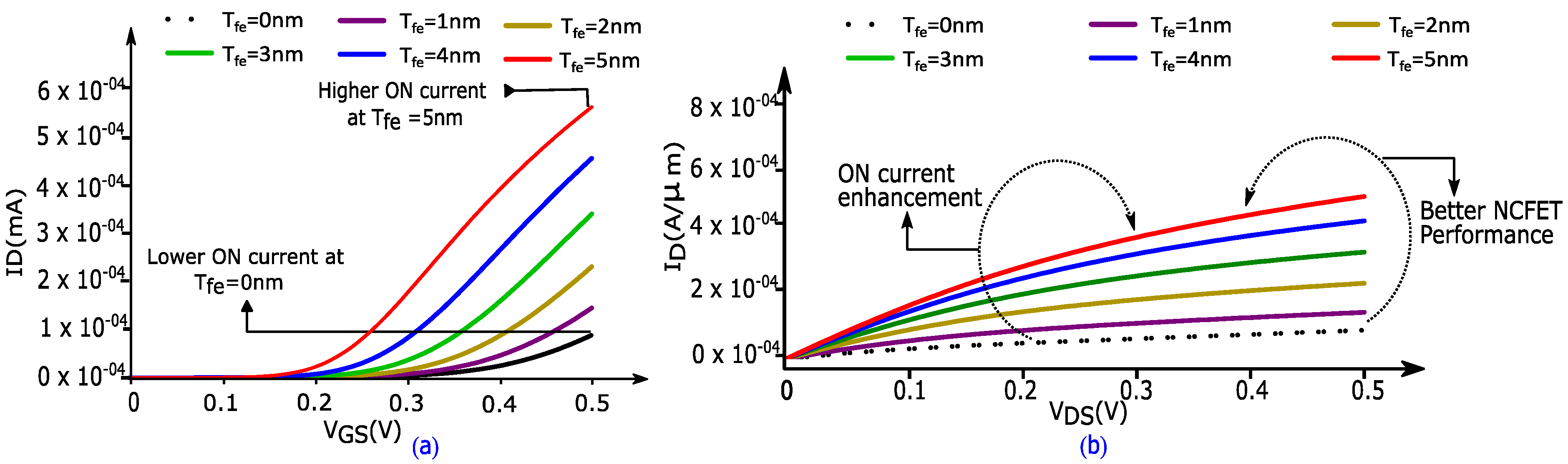
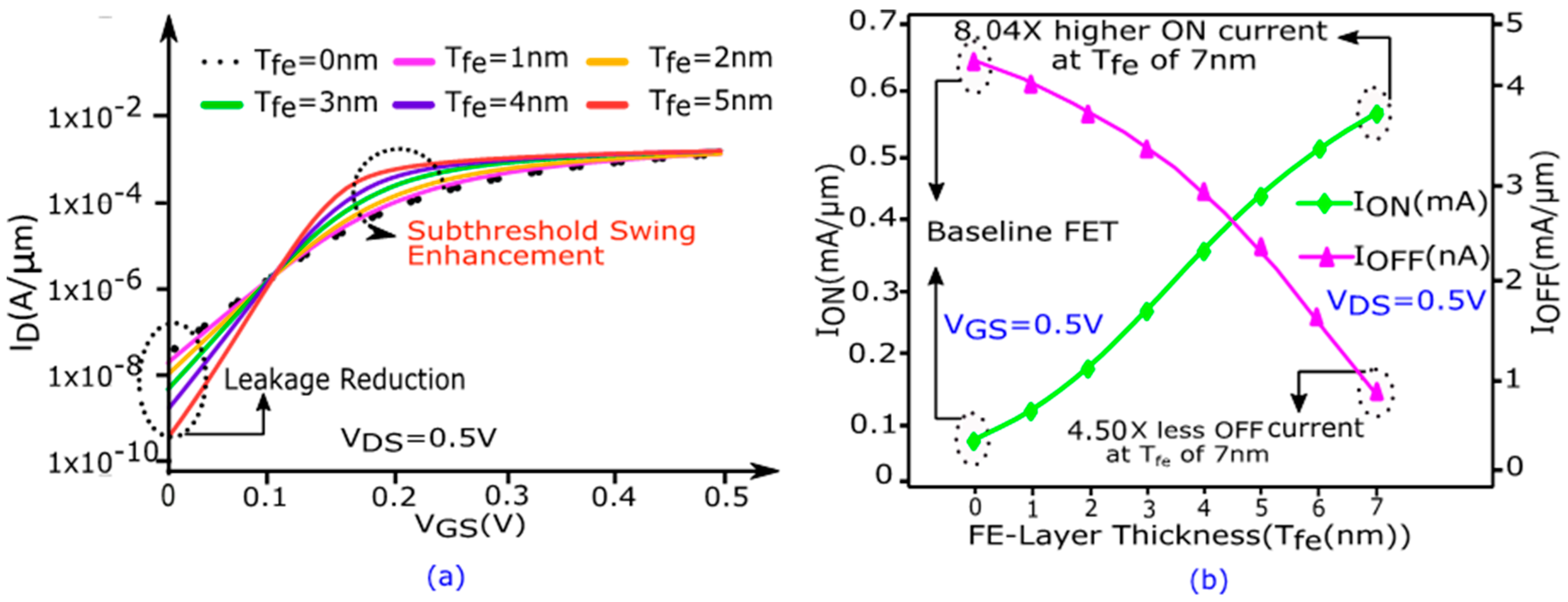
3. NCFET Device Structure and Model Description

This section further describes the construction, workings, and model description of an NCFET device. NCFET device I-V characteristics have been explored by varying ferroelectric thicknesses (Tfe), and they determined the optimal thickness for energy efficient logic circuits.
Figure 1a shows the NCFET device structure, demonstrated by this study, which incorporates a ferroelectric material sandwiched between two metallic layers, thereby resulting in the formation of an analogous negative capacitor. Further, the capacitor obtained is integrated with the baseline CMOS design, incorporating the capacitor divider circuit model of the NCFET device presented in Figure 1b. An equivalent capacitive circuit has been used to determine the internal voltage amplification (Av) described using Equation (1) [16]. The ferroelectric capacitance (Cfe) is represented as the differential ratio of the gate charge density (Q) and potential drop (Vfe), and this capacitance is proportional to 1/Tfe [48].
A V = C f e C f e C i n t
where Cfe is ferroelectric capacitance and Cint is internal capacitance.
C f e = Q V f e = 1 T f e ( 2 α + 12 β Q 2 + 30 γ Q 4 )
When the ferroelectric capacitance (|Cfe|) is greater than (by increasing the Tfe) the internal capacitance of CMOS (Cint), then the NCFET provides higher ON current (ION), leading to lowering subthreshold swing. In addition, the NCFET exhibits hysteresis features when |Cfe| is less than Cint [27]. The value of Tfe (which inversely varies with |Cfe|) must be carefully chosen in order to ensure hysteresis-free behavior and optimal device performance. The NCFET circuit design in this study makes use of a well-known NCFET model created by the MIT research team. This model uses the Intel 40 nm p-type/n-type bulk baseline Si-CMOS and the L-K equation to describe ferroelectric capacitors (FE capacitors). The precise specifications of the NCFET device have been summarized in Table 1.
Figure 2a,b show the I-V characteristics of the n-channel NCFET device with varying Tfe in comparison to the baseline CMOS (in this work, Tfe = 0 nm has been utilized as the baseline CMOS). It demonstrates that the NCFET has shown superior ON current and enhanced performance at Tfe of 5 nm compared to the baseline CMOS at an operating voltage of 0.5 V.
Figure 3a demonstrates ID-VGS characteristics (Log scale) using different Tfe at an operating voltage of 0.5 V. The results show that the NCFET exhibits a lower leakage current (IOFF) compared to the baseline CMOS. This leads to a reduction in subthreshold swing (SS) from 104.7 mV/dec (baseline CMOS) to less than 60 mV/dec.
The ON current (ION) increases and the OFF current (IOFF) decreases as the Tfe values range from 0 nm to 7 nm at VDS = 0.5 V, as illustrated in Figure 3b. In comparison to the baseline CMOS, the NCFET shows a significant improvement, which is ~8.04 × higher in the ON current and ~4.50 × lower in the OFF current with a thickness of 7 nm. Therefore, in comparison to the baseline CMOS device, the NCFET device demonstrates a higher ION/IOFF ratio.

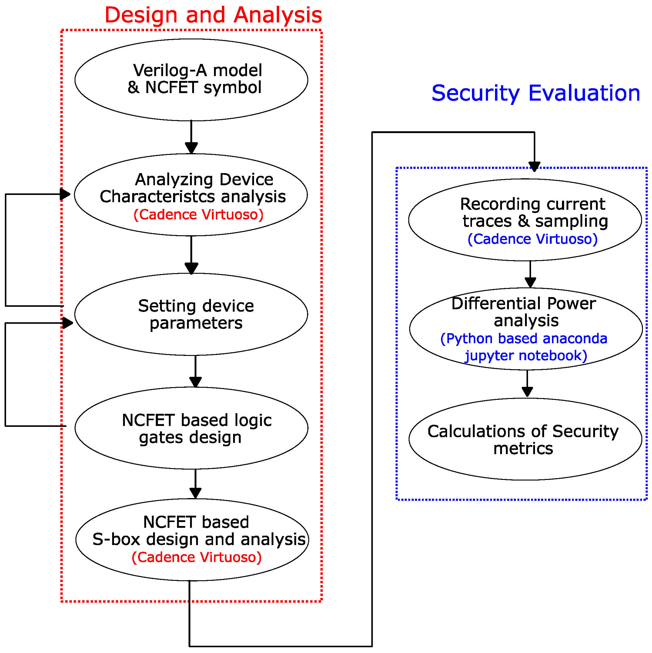
4. Experimental Setup for the NCFET-Based S-Box Design and Security Evaluation Methodology

The flowchart of the NCFET-based logic circuit/S-box for cipher design and DPA evaluation methodology utilized in this study is presented in Figure 4. This study utilizes the Cadence Spectre tool with a Verilog-A model to analyze the performance of the NCFET device/circuit.
The next step involves converting the device model into symbols for circuit design. The exploration of this symbol has led to the design and verification of NCFET-based standard logic gates, including the NCFET 2-input AND, OR, and XOR gates. Utilizing the same design approach, an S-box for the SLIM cipher/circuit has been created using NCFET logic gates. The performance of the NCFET cipher against differential power analysis was assessed by capturing current traces while feeding a stream of data inputs to the cipher. The traces collected are sampled and stored utilizing the Cadence Virtuoso tool. Moreover, the existing traces are analyzed, and differential power analysis (DPA) is conducted to assess the effectiveness of the cipher design. This analysis is conducted in the Python 3 programming language using the Anaconda Jupyter Notebook 6.3.0.

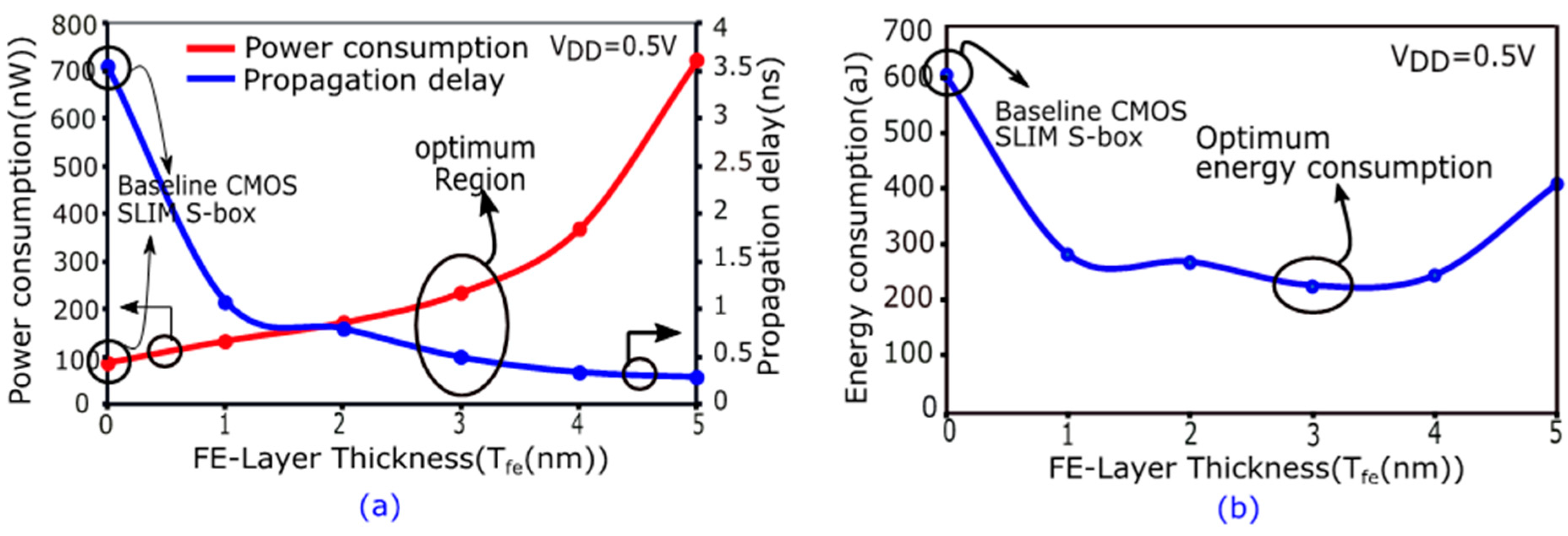
5. Design of an NCFET-Based S-Box for a Lightweight SLIM Block Cipher for Energy Efficiency

This section presents the design and analysis of the SLIM lightweight block cipher using the NCFET. In addition, a comparison is made between the performance of the SLIM cipher based on the NCFET and the standard CMOS design.

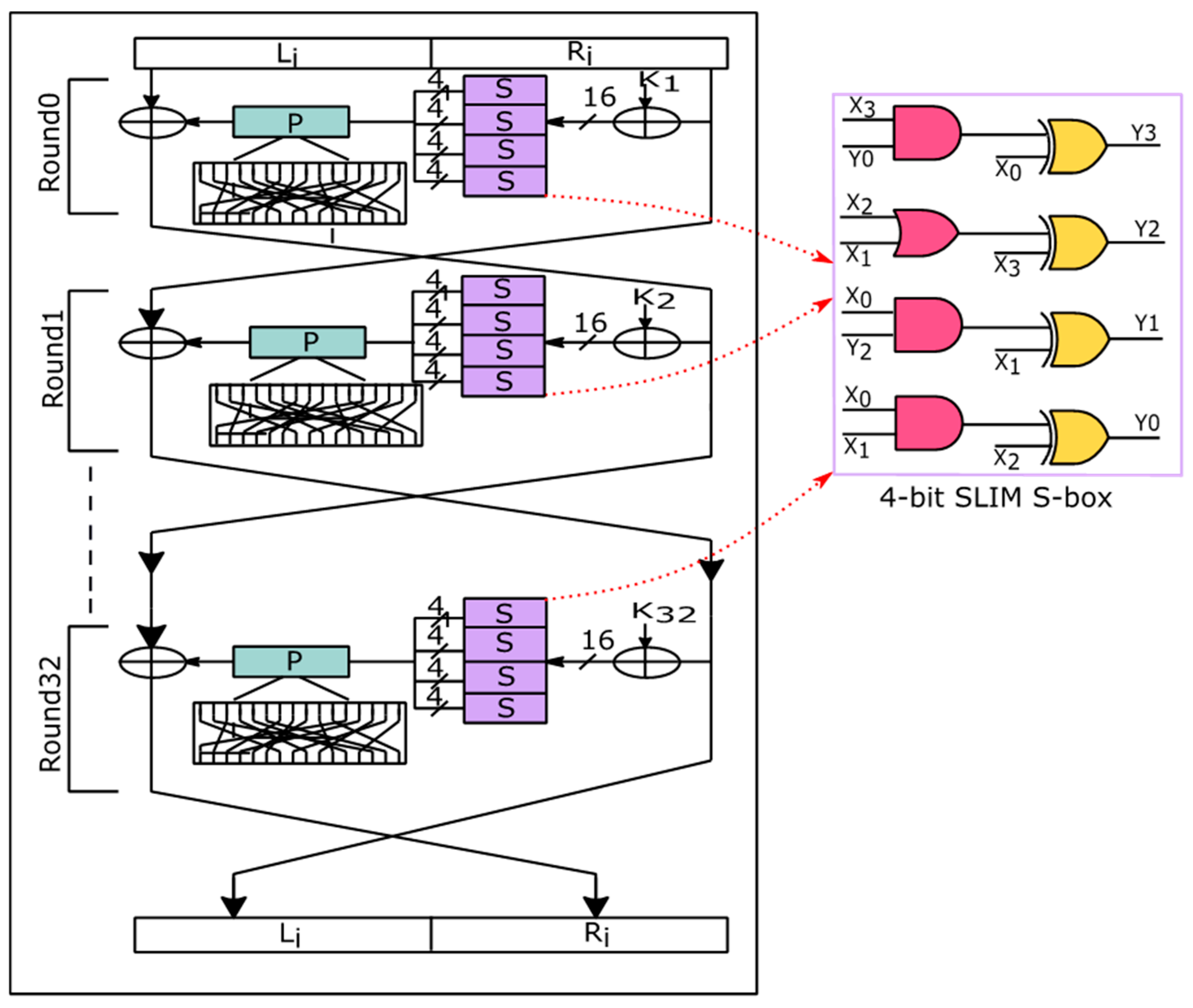
5.1. Structure of the SLIM Lightweight Block Cipher

SLIM is a lightweight block cipher based on the Feistel network with a 32-bit input/output and an 80-bit key for encryption. The complete SLIM architecture is based on the Feistel network structure for enhanced hardware security in terms of DPA attack resiliency as shown in Figure 5. The input is split into two parts, the right half and the left half, which undergoes multiple rounds along with the sub-keys generated. The complete encryption process of the SLIM cipher is performed in 32 rounds. The main components of each round in this process include XOR operations with a round key, 4-bit parallel substitution box (S-box) operations, and subsequent permutations and linear operations [48].

5.2. The NCFET-Based SLIM S-Box Design

SLIM effectively combines the ideas of confusion and diffusion by employing a tiny 4-bit S-box with high non-linearity features. It is well known that S-box designs are the only non-linear elements of the block ciphers and the primary targets for many cryptographic attacks. The SLIM S-box is a combinational block having four inputs (X3-X0) and four outputs (Y3-Y0), as shown in Figure 6.
The SLIM S-box is a combinational block having four inputs (X3-X0) and four outputs (Y3-Y0), as shown in Figure 6a. Figure 6b–d represent the NCFET-based two-input AND, XOR, and OR logic gates design.
The Boolean Equations (3)–(6) are used to express the relationship between inputs and outputs.
Y 3 = X 0   X 3   . Y 0
Y 2 = X 3   ( X 2   + X 1 )
Y 1 = X 1   X 0   . Y 2
Y 0 = X 2   X 0   . X 1
In the above equations, when the inputs X3 X2 X1 X0 = 1110, then the corresponding outputs are Y3 Y2 Y1 Y0 = 1011. Figure 7 shows the transient response of the 4-bit NCFET-based SLIM S-box at a supply voltage of 0.5 V.
Figure 8a depicts the power consumption and propagation delay of the NCFET-based SLIM S-box with different Tfe at VDD = 0.5 V. It can be observed that the propagation delay of the NCFET S-box design significantly reduces as Tfe increases due to the steeper slope of the NCFET. Furthermore, the power consumption of the NCFET S-box design significantly increases as Tfe increases due to the addition of negative capacitance to the gate stack of the baseline SLIM S-box. Figure 8b represents the energy consumption of the NCFET-based SLIM S-box with different Tfe at VDD = 0.5 V. It can be seen that by varying Tfe, the NCFET-based SLIM S-box consumes less energy due to lower propagation delay as compared to the baseline SLIM S-box. It can be observed that the NCFET-based SLIM S-box design shows ~2.65× lower optimum energy consumption at a Tfe of 3 nm compared to the baseline CMOS-based SLIM S-box.
Figure 9a illustrates the relationship between power consumption and propagation delay in the NCFET-based 1 round of the SLIM cipher design across various Tfe values at a VDD of 0.5 V. It can be observed that the propagation delay of the NCFET-based 1 round of the SLIM cipher design significantly reduces as Tfe increases due to the steeper slope of the NCFET. Furthermore, the power consumption of the NCFET-based 1 round of SLIM cipher escalates as Tfe increases, which is attributed to the incorporation of negative capacitance into the gate stack of the baseline MOSFET. Figure 9b explores the energy consumption of the NCFET-based 1 round of the SLIM cipher design with different Tfe at VDD = 0.5 V. It demonstrates that by varying Tfe, the NCFET-based SLIM cipher design consumes less energy due to lower propagation delay as compared to the baseline SLIM cipher design. It can be observed that at a Tfe of 3 nm, the NCFET-based SLIM cipher design shows ~4.25× lower optimum energy consumption in comparison to the baseline CMOS-based SLIM cipher design.

6. Security Assessment of the NCFET-Based S-Box for the Ultra-Lightweight SLIM Cipher Against DPA Attacks and Performance Benchmarking

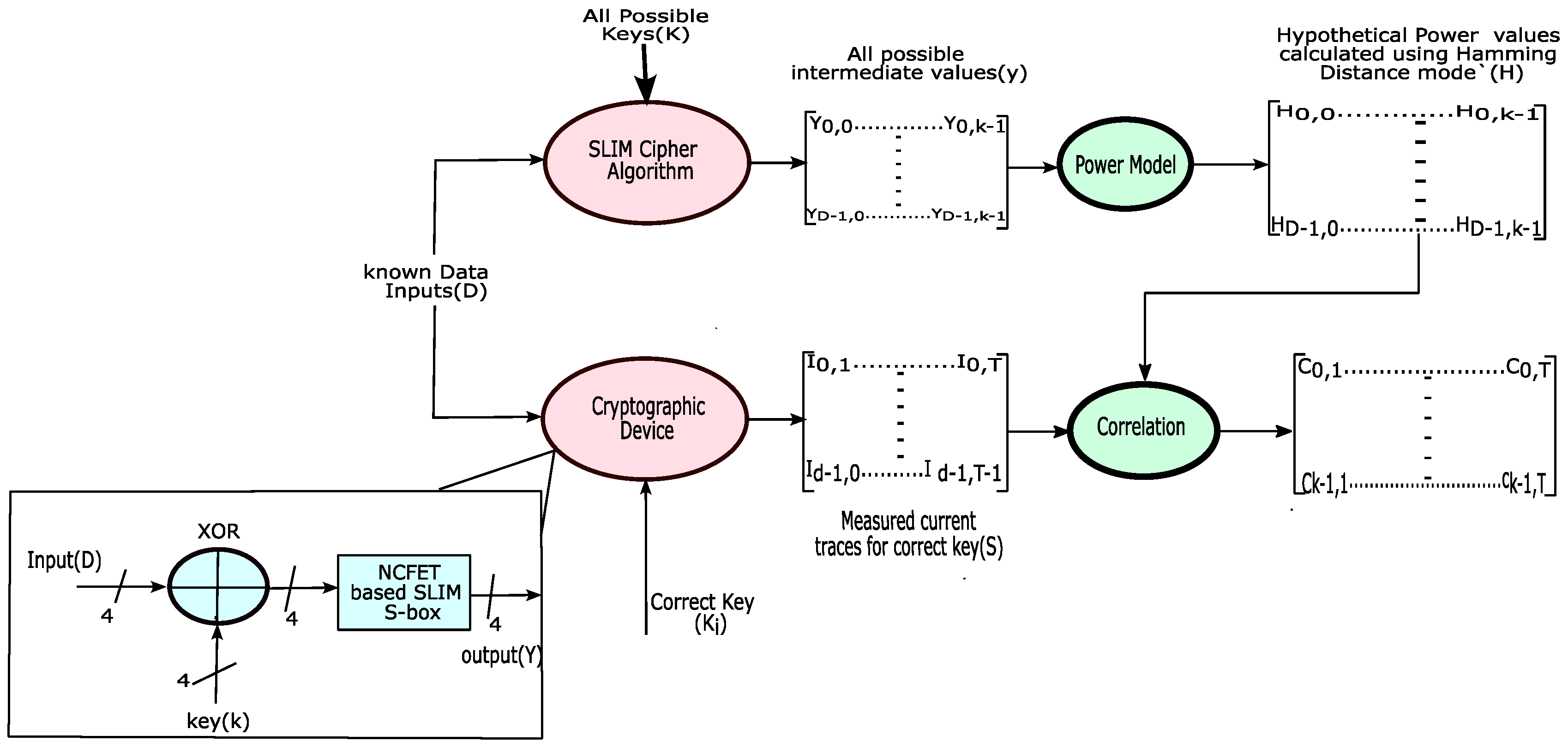
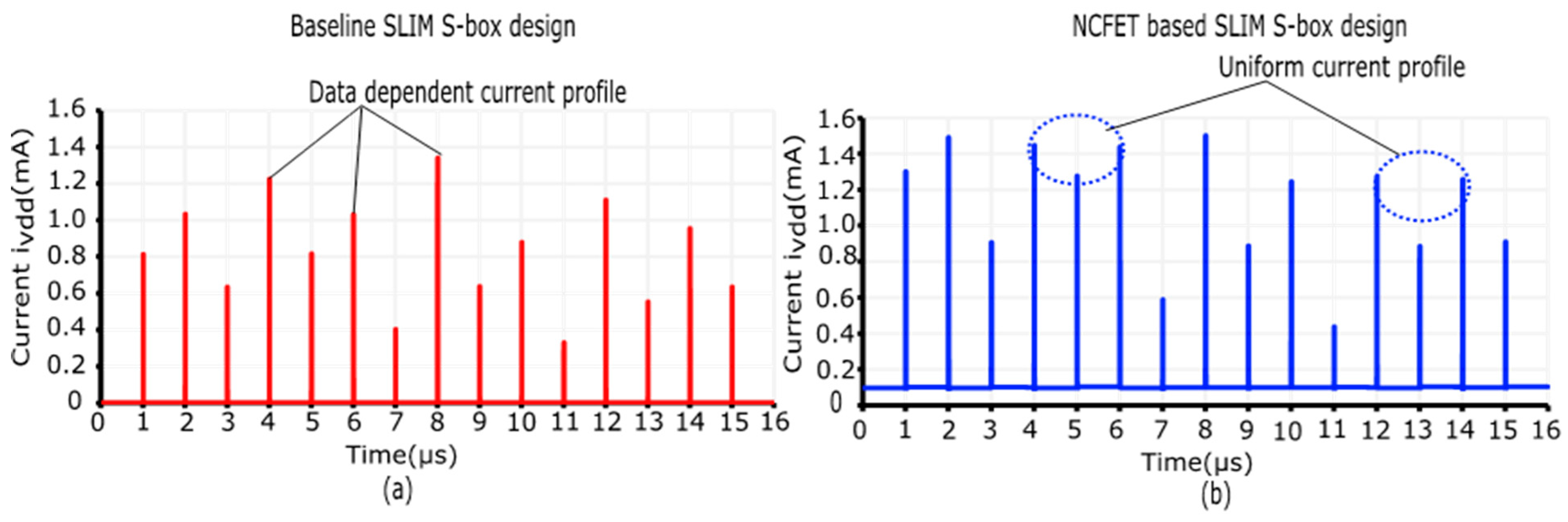
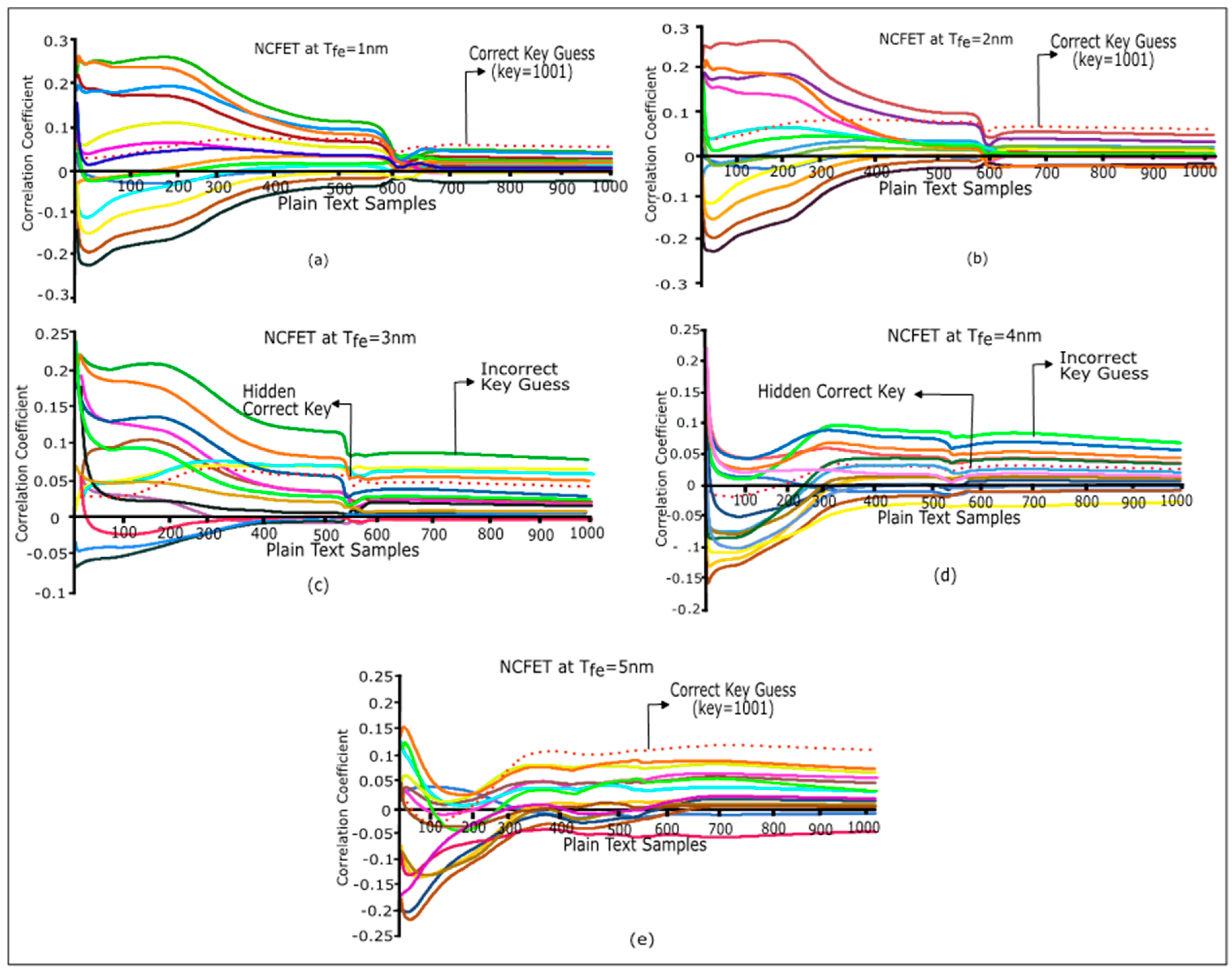
6.1. DPA Attack Methodology on an NCFET-Based S-Box for an Ultra-Lightweight SLIM Cipher

Figure 9 depicts an NCFET-based DPA attack on a SLIM cipher. DPA is a side channel attack that performs correlation analysis considering power traces of cryptographic engines to obtain hidden secret key information. In cryptographic devices, the S-box is the target of the attacker in DPA. The S-box uses a substitution operation to create a comparable 4-bit output from a 4-bit input.
The DPA attack is performed on the SLIM S-box design, which is shown in Figure 10. The detailed DPA attack mechanism is explained as follows.
  • The S-box is first designed in the Cadence Virtuoso environment, followed by the recording of the current traces (iVdd) using random inputs (D) and a fixed key (Ki).
  • The current traces are recorded at a sampling rate of T (T samples per trace) and organized into a matrix S with dimensions of D × T.
  • Next, the S-box algorithm will be implemented using Python 3 to calculate the output values with inputs D (the same inputs as in the previous step) and all potential keys K.
  • The output values are mapped to hypothetical power consumption values through the Hamming Distance (HD) model and organized in a matrix H with dimensions D × K. The Hamming Distance between two consecutive output values is determined using Equation (7).
    HD = Hamming weight (Yi−1⊕Y)
  • Finally, every column of the H matrix is correlated with all the columns of the current trace matrix S.
Figure 11a,b show sample power traces recorded from the baseline SLIM S-box and the NCFET-based SLIM S-box at VDD = 0.5 V. It can be observed that the power traces of the NCFET-based SLIM S-box design deviate significantly from those of the baseline SLIM S-box design. Further, the NCFET-based SLIM S-box exhibits data-independent power traces. This is due to the fact that the NCFET shows more non-linearity in dynamic power consumption due to the increased overall capacitance. By processing the collected power traces, a DPA attack has been performed on the SLIM S-box design.
Figure 12 demonstrates the correlation coefficient characteristics of the SLIM S-box considering 16 power traces by varying Tfe from 0 nm (baseline CMOS) to 5 nm. The original key (1001) is depicted as a dotted line to differentiate it from all other wrong key guesses. The correlation coefficients of the baseline CMOS-based SLIM S-box with all possible keys are shown in Figure 11a. The DPA attack on the baseline CMOS-based SLIM S-box is notably successful with the highest correlation for the original key (K = 1001) when only 16 power traces are evaluated. This illustrates that the baseline CMOS-based S-box is extremely susceptible to DPA attacks, as the original key can be extracted using only 16 power traces.
However, the DPA attack conducted on the NCFET-based SLIM S-box with Tfe ranging from 1 nm to 5 nm was not successful, as shown in Figure 12b–f. The DPA attack on the NCFET-based SLIM S-box (with Tfe ranging from 1 nm to 5 nm) fails with 16 power traces, demonstrating the higher resilience of the NCFET-based SLIM S-box against DPA. Furthermore, a similar DPA attack is carried out on the NCFET-based SLIM S-box with increasing the number of power traces (32, 48, 64, 128 power traces).
Figure 13 represents the correlation coefficient of the NCFET-based SLIM S-box considering 256 power traces by varying Tfe from 1 nm to 5 nm. Based on the analysis, the DPA attack has been found to be effective against the NCFET-based SLIM S-box when using 256 power traces. The correlation coefficients of the NCFET-based SLIM S-box with all possible keys are shown in Figure 13. Notably, when 256 power traces are evaluated, the DPA attack on the NCFET-based SLIM S-box is successful at a Tfe of 1 nm, 4 nm, and 5 nm, as shown in Figure 13a,b,e. Additionally, the DPA attack on the NCFET-based SLIM S-box with a Tfe of 3 nm and 4 nm fails with 256 power traces, demonstrating the higher resilience of the NCFET-based SLIM S-box against DPA, as shown in Figure 13c,d. As a result, the DPA attack on the NCFET-based SLIM S-box is successful with 256 power traces, while the DPA attack on the baseline CMOS-based SLIM S-box fails with only 16 power traces. As a result, the attack effort ratio for DPA is raised to approximately 16 times, making the NCFET-based SLIM S-box more resistant.

6.2. Performance Benchmarking of the Proposed Ultra-Lightweight NCFET-Based SLIM S-Box Design

This section presents the important performance metrics to quantify the resiliency of the proposed S-box design against DPA attacks. The parameters considered are the following.

6.2.1. Signal-to-Noise Ratio (SNR)

This can be described as the ratio between the correlation value of the correct key and the second-highest value of an incorrect key guess, as illustrated in Equation (8) [49]. In order to enhance resilience against DPA, it is essential to calculate the SNR to find the optimal Tfe value. A high level of robustness against DPA attacks is indicated by a lower SNR value in the S-box. Additionally, the SNR plays a crucial role in determining the degree of challenge in discerning between the correct key and an incorrect key guess.
S N R = C o r r e l a t i o n   o f   t h e   c o r r e c t   k e y S e c o n d   m a x i m a l   v a l u e   o f   w r o n g   k e y   g u e s s
The NCFET-based SLIM S-box SNR analysis obtained higher DPA resilience for optimum Tfe. From Figure 14, it can be observed that the SNR value of the NCFET-based SLIM S-box varies with the thickness of the FE layer (Tfe). Moreover, when increasing the Tfe, the SNR value is reduced. Thus, the NCFET-based SLIM cipher demonstrates increased resistance to DPA with a Tfe of 4 nm. (because the lower SNR is less vulnerable to the attacker and is highly resilient). The SNR value of the NCFET-based SLIM S-box is ~3.7× times lower than the baseline CMOS-based SLIM S-box with 256 traces.

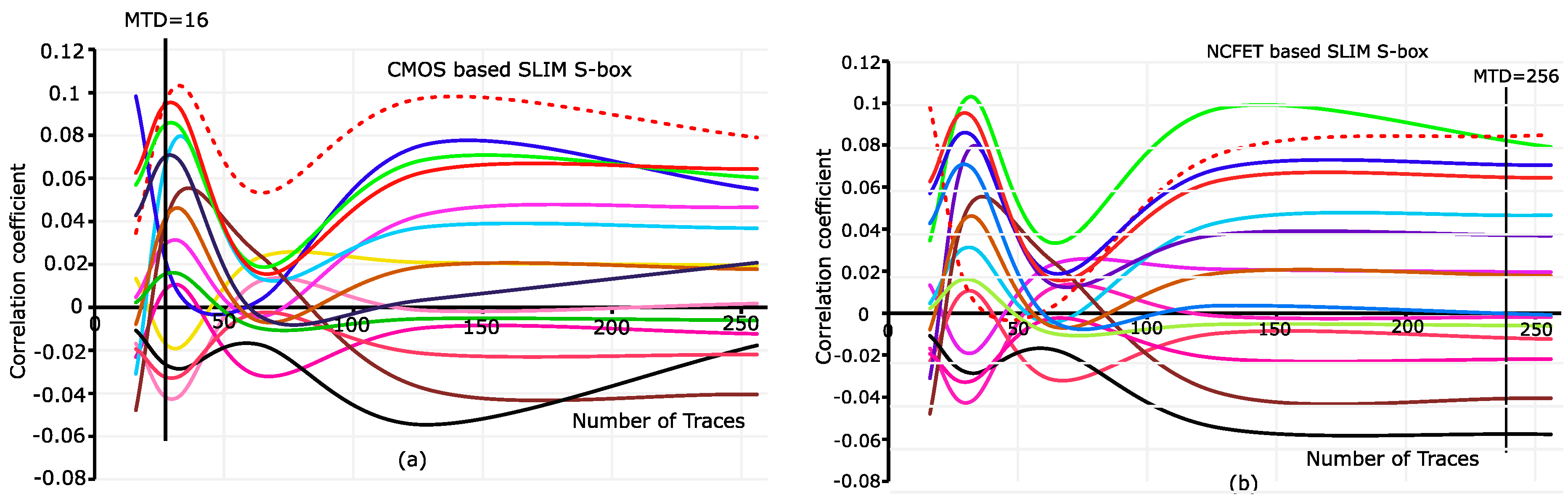
6.2.2. Measurements to Disclosure (MTD)

This can be defined as the point at which the correlation coefficient of the correct key intersects with the highest correlation coefficient among all incorrect key guesses [50]. It also represents the MTD value, which indicates how robust the S-box is against a DPA attack as shown in Figure 15. A higher value of MTD indicates more robustness. Additionally, in Figure 15b, the MTD value of the NCFET-based SLIM S-box design is 16× higher than the CMOS-based SLIM S-box design depicted in Figure 15a.
The MTD value indicates how robust the S-box is against a DPA attack. A higher value of MTD indicates more robustness. Figure 15a represents the MTD value of the CMOS-based SLIM S-box and Figure 15b represents the MTD value of the the NCFET-based SLIM S-box. From this analysis, the attacker effort ratio of the NCFET-based SLIM S-box design increased 16 times compared to the CMOS-based SLIM S-box design as shown in Figure 16a.

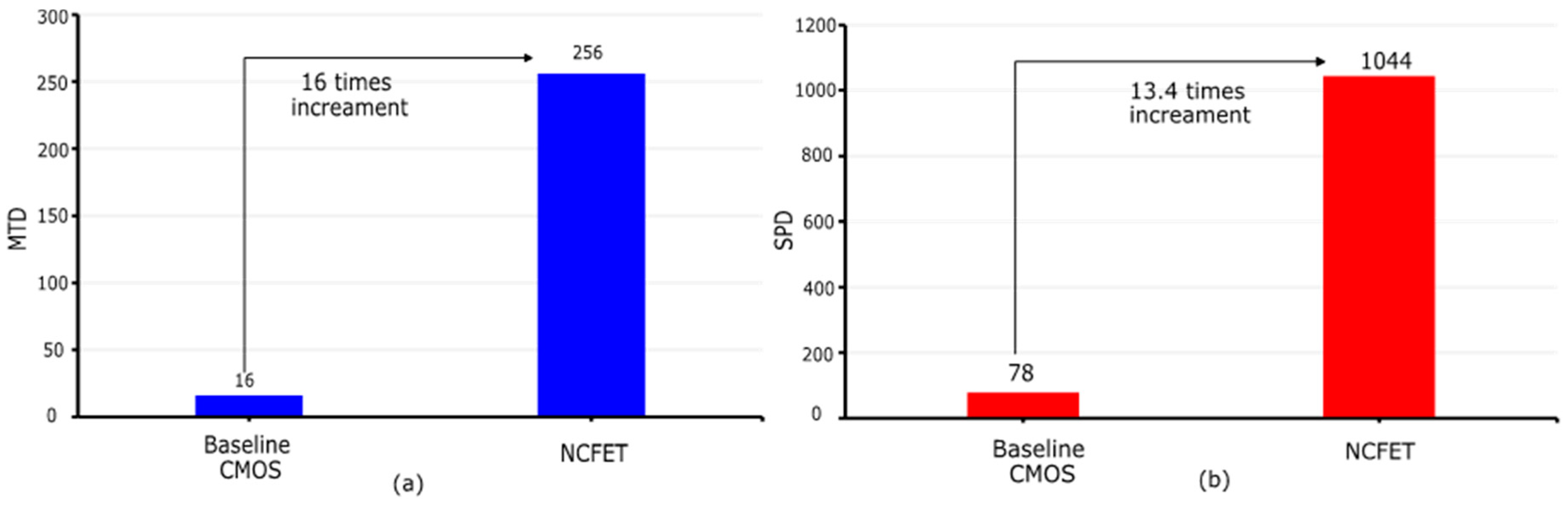
6.2.3. Security Power Delay (SPD)

This metric has been utilized to assess the balance between security outcomes and system performance [51]. The security power delay (SPD) figure of merit, defined by Equation (9), evaluates the balance among security, power consumption, and timing performance, as indicated by the delay value. However, this metric is only relevant when the system is deemed sufficiently secure for use in cryptographic hardware applications. The trade-off between security and performance improves as the SPD value increases.
S P D = M T D ( P o w e r × D e l a y )
Furthermore, Figure 16b describes that the SPD value of the NCFET-based SLIM S-box design is ~13.4× higher than the CMOS-based SLIM S-box design as shown in Figure 16b.
Table 2 depicts the performance comparison of the NCFET-based SLIM S-box with some state-of-the-art S-box designs. The attack effect ratio of the NCFET-based SLIM S-box design is 16× better than the baseline CMOS-based SLIM S-box design. Similarly, the SNR value of the NCFET-based SLIM S-box design is 3.7× lower than the CMOS-based SLIM S-box design. Additionally, the MTD value of the NCFET-based SLIM S-box design is 16× higher than the CMOS-based SLIM S-box design and ~3.3× higher than the FinFET-based PRIDE S-box [9]. Furthermore, the SPD of the NCFET-based SLIM S-box design achieves more than the state-of-the-art CMOS-based S-box designs [9,51].

7. Conclusions

In this paper, the potential challenges of using NCFETs for energy efficient and secure S-box design used in lightweight ciphers exploring the Feistel network structure are demonstrated at VDD = 0.5 V. Performance benchmarking of the proposed NCFET-based S-box design of the Feistel network SLIM cipher with the baseline CMOS SLIM cipher and other existing NCFET PRESENT Cipher with Substitution and Permutation (SPN) networks has been demonstrated. The proposed NCFET S-box design exploits the unique steep slope device characteristics and increases non-linearity in power traces caused by the extra gate capacitance of the NCFETs along with the highly secure Feistel network structure to enhance overall energy efficiency and DPA attack resiliency. A thorough DPA resiliency analysis of the proposed S-box design with performance metrics such as SNR, MTD, and SPD performance comparison with the baseline CMOS design and other state-of-the-art S-box designs has been performed. The MTD value of the NCFET-based SLIM S-box design is ~16× higher than the equivalent CMOS-based SLIM S-box design and ~3.3× higher than the FinFET-based PRIDE S-box design. Furthermore, the SPD value of the NCFET-based SLIM S-box design is better than the state-of-the-art CMOS-based S-box designs. Though NCFETs show promising benefits for hardware security, they still suffer from several issues and have difficulty with the integration of thick traditional ferroelectric material. Hence, many research efforts are still required to further improve the performance of the NCFET through channel engineering, exploring different structural engineering, ferroelectric materials, and optimizing materials parameters, which may enable the rapid commercialization of NCFET-based devices for secure edge devices in the near future. Future device engineering efforts make NCFET-based systems a reality and show lower energy consumption with enhanced hardware security.

Author Contributions

Conceptualization, R.V.; methodology, K.R.P., V.G. and R.V.; software, V.G.; validation, R.V. and V.G.; formal analysis, R.V. and K.R.P.; investigation, K.R.P.; resources, V.G.; data curation, R.V. and K.R.P. writing—original draft preparation, K.R.P. and R.V.; writing—review and editing, V.G. and R.V.; visualization, R.V. and V.G.; supervision, R.V. and V.G.; project administration, R.V. and V.G.; funding acquisition, V.G. and K.R.P. All authors have read and agreed to the published version of the manuscript.

Funding

Financial support was provided by the “Symbiosis Centre for Medical Image Analysis, Symbiosis International (Deemed University)” and “SRM University AP” for the publication of this research.

Data Availability Statement

All the findings made in this study are fully detailed within the paper itself.

Conflicts of Interest

The authors declare no conflicts of interest.

References

  1. Ha, G.; Chen, H.; Jia, C.; Li, M. Threat model and Defense scheme for side-channel attacks in client-side deduplication. Tsinghua Sci. Technol. 2023, 28, 1–12. [Google Scholar] [CrossRef]
  2. Tiwari, U.; Vollala, S.; Ramasubramanian, N.; Begum, B.S. Efficient hardware realization and high radix implementation of modular multi exponential techniques for public key cryptography. Microelectron. J. 2022, 128, 105548. [Google Scholar] [CrossRef]
  3. Wang, W.; Han, J.; Cheng, X.; Zeng, X. An energy-efficient crypto-extension design for RISC-V. Microelectron. J. 2021, 115, 105165. [Google Scholar] [CrossRef]
  4. Japa, A.; Sahoo, S.K.; Vaddi, R.; Majumder, M.K. Emerging tunnel FET and spintronics-based hardware-secure circuit design with ultra-low energy consumption. J. Comput. Electron. 2022, 22, 178–189. [Google Scholar] [CrossRef]
  5. Mishra, N.; Pandya, S. Internet of Things applications, security challenges, attacks, intrusion detection, and future visions: A systematic review. IEEE Access 2021, 9, 59353–59377. [Google Scholar] [CrossRef]
  6. Zaky, A.; Elmitwalli, E.; Hemeda, M.; Ismail, Y.; Salah, K. Ultra low-power encryption/decryption core for lightweight IoT applications. In Proceedings of the ICENCO 2019—2019 15th 2019 15th International Computer Engineering Conference, Cairo, Egypt, 29–30 December 2019; pp. 39–43. [Google Scholar] [CrossRef]
  7. Yli-Mayry, V.; Ueno, R.; Miura, N.; Nagata, M.; Bhasin, S.; Mathieu, Y.; Graba, T.; Danger, J.L.; Homma, N. Diffusional side-channel leakage from unrolled lightweight block ciphers: A case study of power analysis on prince. IEEE Trans. Inf. Forensics Secur. 2021, 16, 1351–1364. [Google Scholar] [CrossRef]
  8. Bronchain, O.; Durvaux, F.; Masure, L.; Standaert, F.X. Efficient profiled side-channel analysis of masked implementations, extended. IEEE Trans. Inf. Forensics Secur. 2022, 17, 574–584. [Google Scholar] [CrossRef]
  9. Delgado-Lozano, I.M.; Tena-Sanchez, E.; Nunez, J.; Acosta, A.J. Design and analysis of secure emerging crypto-hardware using HyperFET devices. IEEE Trans. Emerg. Top. Comput. 2020, 9, 787–796. [Google Scholar] [CrossRef]
  10. Padmini, C.; Ravindra, J.V.R. Design of leakage resilient and DPA attack immune architecture of S BOX. In Proceedings of the 2021 6th International Conference on Communication and Electronics Systems, ICCES 2021, Coimbatre, India, 8–10 July 2021; pp. 936–944. [Google Scholar] [CrossRef]
  11. Masoumi, M. Novel hybrid CMOS/Memristor implementation of the AES algorithm robust against differential power analysis attack. IEEE Trans. Circuits Syst. II Express Briefs 2020, 67, 1314–1318. [Google Scholar] [CrossRef]
  12. Arya, N.; Soni, T.; Pattanaik, M.; Sharma, G.K. Area and energy efficient approximate square rooters for error resilient applications. In Proceedings of the 2020 33rd International Conference on VLSI Design and 2020 19th International Conference on Embedded Systems, Bangalore, India, 4–8 January 2020; pp. 90–95. [Google Scholar] [CrossRef]
  13. Liu, Y.; Qian, K.; Wang, K.; He, L. Effective scaling of blockchain beyond consensus innovations and moore’s law: Challenges and opportunities. IEEE Syst. J. 2022, 16, 1424–1435. [Google Scholar] [CrossRef]
  14. Japa, A.; Majumder, M.K.; Sahoo, S.K.; Vaddi, R. Low area overhead DPA countermeasure exploiting tunnel transistor-based random number generator. IET Circuits Devices Syst. 2020, 14, 640–647. [Google Scholar] [CrossRef]
  15. Kumar, S.D.; Thapliyal, H. Exploration of non-volatile MTJ/CMOS circuits for DPA-resistant embedded hardware. IEEE Trans. Magn. 2019, 55, 1–8. [Google Scholar] [CrossRef]
  16. Amrouch, H.; Van Santen, V.M.; Pahwa, G.; Chauhan, Y.; Henkel, J. NCFET to rescue technology scaling: Opportunities and challenges. In Proceedings of the 2020 25th Asia and South Pacific Design Automation Conference (ASP-DAC), Beijing, China, 13–16 January 2020; pp. 637–644. [Google Scholar] [CrossRef]
  17. Bheemana, R.C.; Japa, A.; Yellampalli, S.; Vaddi, R. Steep switching NCFET based logic for future energy efficient electronics. In Proceedings of the 2021 IEEE International Symposium on Smart Electronic Systems (iSES), Jaipur, India, 18–22 December 2021; pp. 327–330. [Google Scholar] [CrossRef]
  18. Tu, L.; Wang, X.; Wang, J.; Meng, X.; Chu, J. Ferroelectric negative capacitance field effect transistor. Adv. Electron. Mater. 2018, 4, 1800231. [Google Scholar] [CrossRef]
  19. Fan, C.C.; Cheng, C.H.; Chen, Y.R.; Liu, C.; Chang, C.Y. Energy-efficient HfAlOx NCFET: Using gate strain and defect passivation to realize nearly hysteresis-free sub-25mV/dec switch with ultralow leakage. In Proceedings of the 2017 IEEE International Electron Devices Meeting (IEDM), San Francisco, CA, USA, 2–6 December 2018; pp. 23.2.1–23.2.4. [Google Scholar] [CrossRef]
  20. Jo, J.; Shin, C. Experimental observation of voltage amplification using negative capacitance for sub-60 mV/decade CMOS devices. Curr. Appl. Phys. 2015, 15, 352–355. [Google Scholar] [CrossRef]
  21. Jooq, M.K.Q.; Moaiyeri, M.H.; Tamersit, K. Ultra-compact ternary logic gates based on negative capacitance carbon nanotube FETs. IEEE Trans. Circuits Syst. II Express Briefs 2021, 68, 2162–2166. [Google Scholar] [CrossRef]
  22. Wang, H.; Yang, M.; Huang, Q.; Zhu, K.; Zhao, Y.; Liang, Z.; Chen, C.; Wang, Z.; Zhong, Y.; Zhang, X.; et al. New insights into the physical origin of negative capacitance and hysteresis in NCFETs. In Proceedings of the 2018 IEEE International Electron Devices Meeting (IEDM), San Francisco, CA, USA, 1–5 December 2019; p. 31. [Google Scholar] [CrossRef]
  23. Salamin, S.; Rapp, M.; Pathania, A.; Maity, A.; Henkel, J.; Mitra, T.; Amrouch, H. Power-efficient heterogeneous many-core design with NCFET technology. IEEE Trans. Comput. 2021, 70, 1484–1497. [Google Scholar] [CrossRef]
  24. Lee, C.H.; Hsu, Y.T.; Liu, T.T.; Chiueh, T.D. Design of an 45nm NCFET based compute-in-SRAM for energy-efficient machine learning applications. In Proceedings of the 2020 IEEE Asia Pacific Conference on Circuits and Systems (APCCAS), Ha Long, Vietnam, 8–10 December 2020; pp. 193–196. [Google Scholar] [CrossRef]
  25. Chauhan, N.; Bagga, N.; Banchhor, S.; Datta, A.; Dasgupta, S.; Bulusu, A. Negative-to-positive differential resistance transition in ferroelectric FET: Physical insight and utilization in analog circuits. IEEE Trans. Ultrason. Ferroelectrics Freq. Control 2022, 69, 430–437. [Google Scholar] [CrossRef]
  26. Liang, Y.; Zhu, Z.; Li, X.; Gupta, S.K.; Datta, S.; Narayanan, V. Utilization of negative-capacitance FETs to boost analog circuit performances. IEEE Trans. Very Large Scale Integr. Syst. 2019, 27, 2855–2860. [Google Scholar] [CrossRef]
  27. Bheemana, R.C.; Japa, A.; Yellampalli, S.S.; Vaddi, R. Negative capacitance FETs for energy efficient and hardware secure logic designs. Microelectron. J. 2022, 119, 105320. [Google Scholar] [CrossRef]
  28. Japa, A.; Majumder, M.K.; Sahoo, S.K.; Vaddi, R.; Kaushik, B.K. Hardware security exploiting post-CMOS devices: Fundamental device characteristics, state-of-the-art countermeasures, challenges and roadmap. IEEE Circ. Syst. Mag. 2021, 21, 4–30. [Google Scholar] [CrossRef]
  29. Birudu, V.; Yellampalli, S.S.; Vaddi, R. A negative capacitance FET based energy efficient 6T SRAM computing-in-memory (CiM) cell design for deep neural networks. Microelectron. J. 2023, 139, 105867. [Google Scholar] [CrossRef]
  30. Keerthi, G.; Semwal, S.; Kranti, A. Analytical modeling of negative capacitance transistor based ultra-low power Schmitt trigger. Solid-State Electron. 2023, 207, 108700. [Google Scholar] [CrossRef]
  31. Choudhuri, B.; Mummaneni, K. A new pocket-doped NCFET for low power applications: Impact of ferroelectric and oxide thickness on its performance. Micro Nanostruct. 2022, 169, 207360. [Google Scholar]
  32. Hassan, R.; Qamar, F.; Hasan, M.K.; Ha, A.; Aman, M.; Ahmed, A.S. Internet of Things and its applications: A comprehensive survey. Symmetry 2020, 12, 1674. [Google Scholar] [CrossRef]
  33. Dash, S.P. The impact of IoT in healthcare: Global review. J. Indian Inst. Sci. 2020, 100, 773–785. [Google Scholar] [CrossRef]
  34. Demestichas, K.; Peppes, N.; Alexakis, T. Survey on security threats in agricultural IoT and smart farming. Sensors 2020, 20, 6458. [Google Scholar] [CrossRef]
  35. Rahim, M.A.; Rahman, M.A.; Rahman, M.M.; Asyhari, A.T.; Bhuiyan, M.Z.A.; Ramasamy, D. Evolution of IoT-enabled connectivity and applications in automotive industry: A review. Veh. Commun. 2021, 27, 100285. [Google Scholar] [CrossRef]
  36. Suryadevara, N.K.; Biswal, G.R. Smart plugs: Paradigms and applications in the smart city-and-smart grid. Energies 2019, 12, 1957. [Google Scholar] [CrossRef]
  37. Ngo, Q.-D.; Nguyen, H.-T.; Nguyen, L.-C.; Nguyen, D.-H. A survey of IoT malware and detection methods based on static features. ICT Express 2020, 6, 280–286. [Google Scholar] [CrossRef]
  38. Khalifa, O.O.; Islam, M.R.; Khan, S.; Shebani, M.S. Communications cryptography. In Proceedings of the 2004 RF and Microwave Conference, Selangor, Malaysia, 5–6 October 2004. [Google Scholar]
  39. Thakor, V.A.; Razzaque, M.A.; Khandaker, M.R.A. Lightweight Cryptography Algorithms for Resource-Constrained IoT Devices: A Review, Comparison and Research Opportunities. IEEE Access 2021, 9, 28177–28193. [Google Scholar] [CrossRef]
  40. Aziz, S.; Shoukat, I.A.; Iftikhar, M.; Murtaza, M.; Alenezi, A.M.; Lee, C.-C.; Taj, I. Next-Generation Block Ciphers: Achieving Superior Memory Efficiency and Cryptographic Robustness for IoT Devices. Cryptography 2024, 8, 47. [Google Scholar] [CrossRef]
  41. Diehl, W.; Abdulgadir, A.; Kaps, J.P.; Gaj, K. Comparing the cost of protecting selected lightweight block ciphers against differential power analysis in low-cost FPGAs. Computers 2018, 7, 28. [Google Scholar] [CrossRef]
  42. Bheemana, R.C.; Japa, A.; Yellampalli, S.S.; Vaddi, R. Negative capacitance FET based energy efficient and DPA attack resilient ultra-light weight block cipher design. Microelectron. J. 2023, 133, 105711. [Google Scholar] [CrossRef]
  43. Kaushal, S. Introduction to Newly Adopted NCFET and Ferroelectrics for Low-Power Application. In Advanced Ultra Low-Power Semiconductor Devices: Design and Applications; Wiley: Hoboken, NJ, USA,, 2023; pp. 207–234. [Google Scholar] [CrossRef]
  44. Japa, A.; Majumder, M.K.; Sahoo, S.K.; Vaddi, R. Tunnel FET-based ultralow-power and hardware-secure circuit design considering p-i-n forward leakage. Int. J. Circuit Theory Appl. 2020, 48, 524–538. [Google Scholar] [CrossRef]
  45. Kwon, D.; Cheema, S.; Shanker, N.; Chatterjee, K.; Liao, Y.H.; Tan, A.J.; Hu, C.; Salahuddin, S. Negative Capacitance FET with 1.8-nm-Thick Zr-Doped HfO2 Oxide. IEEE Electron Device Lett. 2019, 40, 993–996. [Google Scholar] [CrossRef]
  46. Li, X.; Sampson, J.; Khan, A.; Ma, K.; George, S.; Aziz, A.; Gupta, S.K.; Salahuddin, S.; Chang, M.-F.; Datta, S.; et al. Enabling Energy-Efficient Nonvolatile Computing with Negative Capacitance FET. IEEE Trans. Electron Devices 2017, 64, 3452–3458. [Google Scholar] [CrossRef]
  47. Radhakrishna, U.; Khan, P.A.; Tech, G.; Berkeley, U.C. Compact Model of Negative Capacitance CMOSs (NCFETs). 2017. Available online: https://nanohub.org/projects/mvsncfet (accessed on 23 October 2024).
  48. Pahwa, G.; Dutta, T.; Agarwal, A.; Khandelwal, S.; Salahuddin, S.; Hu, C.; Chauhan, Y.S. Analysis and compact modelling of negative capacitance transistor with high ON-current and negative output differential resistance—Part I: Model description. IEEE Trans. Electron. Dev. 2016, 63, 4981–4985. [Google Scholar] [CrossRef]
  49. Aboushosha, B.; Ramadan, R.A.; Dwivedi, A.D.; El-Sayed, A.; Dessouky, M.M. SLIM: A Lightweight Block Cipher for Internet of Health Things. IEEE Access 2020, 8, 203747–203757. [Google Scholar] [CrossRef]
  50. Kumar, S.D.; Thapliyal, H.; Mohammad, A. FinSAL: FinFET-Based Secure Adiabatic Logic for Energy-Efficient and DPA Resistant IoT Devices. IEEE Trans. Comput.-Aided Des. Integr. Circuits Syst. 2018, 37, 110–122. [Google Scholar] [CrossRef]
  51. Tiri, K.; Hwang, D.; Hodjat, A.; Lai, B.C.; Yang, S.; Schaumont, P.; Verbauwhede, I. Prototype IC with WDDL and differential routing–DPA resistance assessment. In International Workshop on Cryptographic Hardware and Embedded Systems; Springer: Berlin/Heidelberg, Germany, 2005; pp. 354–365. [Google Scholar]
  52. Tena-Sánchez, E.; Acosta, A.J. Logic minimization and wide fan-in issues in DPL-based cryptocircuits against power analysis attacks. Int. J. Circuit Theory Appl. 2019, 47, 238–253. [Google Scholar]
Figure 1. NCFET (a) device structure and (b) equivalent capacitor divider circuit model.
Electronics 14 01114 g001
Figure 2. (a) Demonstration of ID-VGS characteristics using different Tfe (b). Demonstration of ID-VDS characteristics using different Tfe.
Electronics 14 01114 g002
Figure 3. (a) Demonstration of ID-VGS characteristics (Log scale) using different Tfe (b) ION and IOFF improvements in NCFETs with different FE thicknesses (Tfe(nm)).
Electronics 14 01114 g003
Figure 4. Experimental setup for the design and security evaluation of the NCFET-based basic logic gates and the S-box for the SLIM cipher design.
Electronics 14 01114 g004
Figure 5. Encryption process of the SLIM cipher using the Feistel network structure [34].
Electronics 14 01114 g005
Figure 6. (a) The NCFET-based 4-bit SLIM S-box design. The NCFET-based two-input logic gates (b) AND, (c) XOR, (d) OR.
Electronics 14 01114 g006
Figure 7. Transient response characteristics of the NCFET-based 4-bit SLIM S-box design.
Electronics 14 01114 g007
Figure 8. (a) Power consumption and propagation delay analysis for the NCFET-based SLIM S-box design by varying Tfe at VDD = 0.5 V; (b) energy consumption analysis for the NCFET-based SLIM S-box design by varying Tfe at VDD = 0.5 V.
Electronics 14 01114 g008
Figure 9. (a) Power consumption and propagation delay analysis for the NCFET 1 round of the SLIM cipher design by varying Tfe at VDD = 0.5 V; (b) energy consumption analysis for the NCFET-based SLIM cipher design by varying Tfe at VDD = 0.5 V.
Electronics 14 01114 g009
Figure 10. A DPA attack mechanism on the NCFET-based S-box for the SLIM cipher.
Electronics 14 01114 g010
Figure 11. Sample power traces (a) of the baseline SLIM S-box design and (b) the NCFET-based SLIM S-box design with VDD = 0.5 V.
Electronics 14 01114 g011
Figure 12. Correlation coefficient of the NCFET-based SLIM S-box design with (a) baseline CMOS (Tfe = 0 nm), (b) Tfe = 1 nm, (c) Tfe = 2 nm, (d) Tfe = 3 nm, (e) Tfe = 4 nm, and (f) Tfe = 5 nm taking 16 power traces with VDD = 0.5 V.
Electronics 14 01114 g012
Figure 13. Correlation coefficient of the NCFET-based SLIM S-box design with (a) Tfe = 1 nm, (b) Tfe = 2 nm, (c) Tfe = 3 nm, (d) Tfe = 4 nm, and (e) Tfe = 5 nm taking 256 power traces with VDD = 0.5 V.
Electronics 14 01114 g013
Figure 14. SNR analysis of the NCFET-based SLIM S-box with varying thicknesses of the Fe layer (Tfe(nm)) at VDD = 0.5 V.
Electronics 14 01114 g014
Figure 15. MTD analysis of the SLIM S-box using (a) baseline CMOS and (b) NCFET at VDD = 0.5 V.
Electronics 14 01114 g015
Figure 16. (a) MTD analysis of the SLIM S-box using the NCFET and baseline CMOS SLIM S-box at VDD = 0.5 V. (b) SPD analysis of the NCFET-based SLIM S-box and baseline CMOS SLIM S-box at VDD = 0.5 V.
Electronics 14 01114 g016
Table 1. Parameters of the NCFET device.
SymbolDevice ParametersValues
LgdrLength of the Gate4.0 × 10−6 cm
WTransistor Width1.0 × 10−6 cm
PoRemnant Polarization2.5 × 102 C/cm2
EcCoercive Field6.5 × 109 V/cm
TfeThickness of the FE Layer5.0 × 10−11 cm
Table 2. Performance benchmark comparison of the NCFET-based SLIM S-box with the state-of-the-art S-box designs.
PRIDE
S-Box [52]
PRIDE
S-Box [52]
PRIDE-Based S-Box with SABL [4]PRIDE-Based S-Box with SABL [4]PRESENT-80 S-Box [44]SLIM S-Box
(This Work)
TechnologyFinFET
14 nm
HyperFET 14 nmTFET 20 nmFinFET
20 nm
NCFET
40 nm
CMOS
40 nm
NCFET
40 nm
VDD (V)0.80.80.30.30.50.50.5
Power consumption (µW)5.045.166.36.70.2540.0850.233
Propagation delay (ns)0.180.522.126.170.513.540.45
Energy consumption (fJ)1.815.3613.0941.3390.2590.6080.228
SNR----------0.7951.10740.298
MTD76.06------6416256
SPD
(1015) J−1
85.83711.36----275781044
Disclaimer/Publisher’s Note: The statements, opinions and data contained in all publications are solely those of the individual author(s) and contributor(s) and not of MDPI and/or the editor(s). MDPI and/or the editor(s) disclaim responsibility for any injury to people or property resulting from any ideas, methods, instructions or products referred to in the content.

