Review

Analysis of Circuit Configurations Suitable for Self-Supplied AC-DC Converters Using Thin-Film Piezoelectric Generators and Multilayer Energy Storage Supercapacitors

1
Department of Electronics, Faculty of Electronic Engineering and Technologies (FEET), Technical University of Sofia, Kliment Ohridski Blvd., 8, 1000 Sofia, Bulgaria
2
Department of Microelectronics, Faculty of Electronic Engineering and Technology (FEET), Technical University of Sofia, Kliment Ohridski Blvd., 8, 1000 Sofia, Bulgaria
*
Author to whom correspondence should be addressed.
Electronics 2025, 14(6), 1083; https://doi.org/10.3390/electronics14061083
Submission received: 11 February 2025 / Revised: 1 March 2025 / Accepted: 7 March 2025 / Published: 9 March 2025

Abstract

:
The improvement of microelectronic technologies and the practical application of some new materials has resulted in the realization of various highly efficient thin-film energy harvesters in the last few years. Self-powered supplies intended to work with thin-film harvesters have been developed. This type of power supply with integrated various thin-film harvesters has proven to be very suitable for providing electrical energy for wearable electronic sensor systems, with practical applications for implementing personalized medicine through continuously monitoring an individual’s state of health. The application of wearable electronics in medicine will become increasingly important in the next few years, as it can support timely decision-making, especially in high-risk patients. This paper presents a review and comparative analysis of the optimal circuit configurations used to design power supply devices with discrete and integrated components, obtaining electrical power from various thin-film piezoelectric generators, and storing electrical energy in low-power multilayer supercapacitors. Based on an analysis of the principle of operation of the selected circuit configurations, analytical expressions for the basic static and dynamic parameters have been obtained, taking into account the peculiarities of their integration with the biomedical signal processing system. Advantages and weaknesses are analyzed through simulation testing for each configuration, as the prospects for improvement are outlined. Also, for each group of circuit configurations, the key parameters and characteristics of recent high-impact papers, especially those focusing on low-power applications, are presented and analyzed in tabular form. As a result of the analysis of the various circuit configurations, some analytical recommendations have been defined regarding the optimal selection of passive and active elements, which can contribute to a better understanding of the design principles of battery-free power supplies converting electrical energy from some specific recently developed thin-film energy harvesters.

1. Introduction

In the last ten years, there has been an increasing application in developing and using various wearable electronic devices [1,2,3,4,5,6,7,8,9,10,11,12,13,14,15]. These electronic devices are often developed as smartwatches. Medical smart sensors are implemented as fitness trackers and headsets with augmented reality. The goal of developing wearable electronic devices is to provide useful functions that are easily and quickly accessible through visual, audio, and tactile elements, as well as to provide opportunities for the wireless transmission of accumulated data from performed measurement procedures. A critical condition for this electronic device is that it must be very well integrated into the human body so that it does not create discomfort when wearing and using it. The most significant applications of wearable devices are electronic health monitoring modules and the ability to wirelessly transmit the results of precise measurements to health centers for analysis and decision-making. The projected annual growth rate of manufactured wearable electronic devices is approximately 13.5%, from 2024 to 2034. The market capitalization is expected to reach around $635.82 billion by 2034 [16]. This growth has stimulated the creation of improvements in the electronic signal processing system and wireless data transmission, as well as the improvement of the electronic modules, providing an uninterrupted power supply with stable electrical parameters. Like the other electronic signal processing systems and power supply devices, they must be very well integrated with the human body without causing discomfort when wearing them. This means that the power supplies, from a structural point of view, have to be sufficiently small and light in weight. Also, the input electrical energy has to be obtained from the environment in certain conditions, and not from the use of standard rechargeable batteries or implanted batteries. Depending on the electrical current consumption, the necessary batteries remain relatively large in overall size, have a fixed energy density, limited operational lifetime (including for implantable batteries—up to a few years), and some of them have chemical side effects [12,17]. Also, the use of batteries in many practical cases is not applicable because some electronic devices require frequent replacement due to higher consumption, or if the location of the battery is difficult to access. Therefore, in the last few years, devices that obtain electrical energy from piezoelectric, triboelectric, thermoelectric, or photovoltaic generators have been increasingly used. Also, some wearable biofuel cells [1,18,19] are used, in which electrical energy is generated through biochemical reactions, usually involving enzymes or microorganisms that catalyze the oxidation of biofuels, such as glucose or lactate, present in body fluids, such as sweat, tears, saliva, and, in some cases, blood. These devices consist of (bio)anodes and (bio)cathodes separated by an electrolyte reservoir containing the biofluid as an electrolyte. The result is a conversion of chemical energy into a constant electrical voltage, similar to standard fuel cells, but in their case, bio-compatible materials and processes are used. When mechanical deformations occur in the piezoelectric or triboelectric generators, an instantaneous AC voltage is produced between the electrodes. In triboelectric generators, based on the effect of electrostatic induction, when two different materials are in contact and separated, an electric charge accumulates between the two electrodes [20,21,22,23]. For the piezoelectric generators, when mechanical vibrations occur, based on the reverse piezoelectric effect, an accumulation of electric charge is also obtained at the two opposite electrodes, and a current flow is obtained when there is a closed loop [6,24,25,26]. The piezoelectric and triboelectric power generators, from an electrical point of view, can be considered as current sources with a relatively large internal resistance, which can reach several MΩ. The output power for piezoelectric generators reaches up to about 10 μW/cm2, and for triboelectric generators it reaches up to 100 μW/cm2 [1,27,28]. When using piezoelectric generators for wearable devices, it is important to note that the frequency of mechanical vibrations reaches about 10–20 Hz. Most often, the frequency of mechanical vibrations is lower than the resonant frequency, and the signal is a complex periodic signal containing multiple spectral components [29,30,31,32]. A polarization voltage can also be obtained for some of the higher harmonics, but with an amplitude lower than the amplitude of the fundamental harmonic. Also, the parameters of the piezoelectric generators can vary significantly when the external force changes, especially when the acceleration amplitude and tip mass change. Moreover, these conditions can, in some cases, be limiting, especially in elderly or at-risk patients with poor mobility. In triboelectric generators, the frequency of mechanical vibrations is also around a few hertz, and they can produce high output-power but from a relatively large area of the energy conversion structure [21,33]. As a result, triboelectric energy harvesters are mainly suitable for athletes or people in a relatively good state of health, in which the main vital parameters are studied during physical exertion, such as running, physical exercises with fitness equipment, and others.
The photovoltaic generators convert sunlight directly into electricity based on the photovoltaic effect. For them, the internal resistance varies from several ohms to several tens of ohms, and the output power can vary from 1 μW/cm2 to 100 μW/cm2 [1,28,34]. In comparison with other structures, photovoltaic generators can provide the highest output power with a relatively small area for energy conversion. Nowadays, a large number of people spend most of their time indoors, where the lighting is not sufficient, and as a result, the efficiency of photovoltaic generators decreases. Also, depending on the specific application, the area of the photovoltaic generator may be unacceptably large for a wearable device. The thermoelectric generators are also very interesting from an application point of view, in which, based on the Seebeck effect, thermal energy is converted into electrical energy. These generators can be considered as DC voltage sources with a small internal resistance of the order of a few ohms. The output electrical power reaches up to 1 μW/cm2 [35,36]. According to the Seebeck effect, when a temperature gradient occurs in a thermoelectric material (containing two different p- and n-type semiconductors that are electrically isolated), the free charge carriers (electrons and holes) diffuse from the hot junction to the cold ends of the two semiconductors. Then, it forms a closed loop electrical current flow. In the context of wearable electronic devices, thermoelectric generators are well-suited due to their ability to use the body’s inherent heat to provide the power supply voltage for the rest of the electronic modules used for signal processing. A weakness of thermoelectric generators and wearable biofuel cells is the relatively low electrical energy that can obtained. Also, wearable biofuel cells sometimes require the use of a relatively large area of the harvester for energy conversion.
In the last few years, energy harvesting systems, which are a specific combination of a piezoelectric, triboelectric, or thermoelectric generator and a low-power (or micro-power) supercapacitor [28,37,38,39], have been generated particular interest. As a result, energy systems of the “all-in-one” type have been obtained, through which a greater value for energy efficiency can be achieved, since the produced electrical energy is directly transferred to the energy storage element. Also, smaller overall sizes can be obtained with this structure, and some simplification of the power conversion interface circuit can be obtained.
An analysis of the available literature shows a vast variety of techniques for designing interface electronic circuits [21,22,27,40,41,42,43,44,45,46,47] that convert electrical energy from the various energy harvesters discussed above in this section. Moreover, the research community’s interest in interface circuits is very high, as most of them need to provide electrical energy for low-power standalone portable and wearable electronic devices. For example, such devices are wireless sensor networks, implantable electronic modules, and Internet-of-Thing sensors, which include various modules, such as low-power sensors, data processing (with ADCs/DACs, MCUs, and programmable SoCs), wireless transmission modules, and, in some cases, low-power display. All these electronic devices, for their efficient operation, mainly require high stability of the supply DC voltage and current in relatively wide temperature ranges, load capacity in a set range, and long-term continuity of the operation. In fact, the interface electronic circuits or power management circuits (PMCs) represent power supplies for portable and wearable electronics that must provide the functionality described above. Under these conditions, in general, the power supplies must have low current consumption, i.e., a high value of energy efficiency. They have to provide impedance matching with the signal source and the energy storage element (such as an electrolytic capacitor or supercapacitor), and include a cold startup circuit with the ability to reduce consumption in dynamic operational mode. Also, they have small sizes and weight to ensure better integration with the rest of the electronic system. The review of the literature showed the lack of systematization of circuit configurations and their suitability for developing low-power or micro-power supply devices. On the one hand, this is due to the difficulty of theoretically enveloping the problem due to the presence of a large number of design approaches and techniques. Also, micro-power supply devices have circuitry that differs significantly from the principles of building power sources that are designed to provide a large output current (>100 mA) and relatively large values for the supply voltage. On the other hand, in the last few years, a relatively large number of commercially available integrated circuits have been developed that have the functionality of low-power devices in a single chip [48,49,50,51]. In many cases, these integrated circuits are suitable and can replace custom electronic circuits. However, there are also several practical cases, such as those described above [37,38,39], where it is not possible to use the commercially available integrated circuits or, depending on the parameters of the energy harvesting generator or the external load, a custom power supply device has to be built with certain electrical and structural parameters [22,23,25,26].
In this work, analyzing the advantages and some disadvantages of various energy harvesters, the piezoelectric elements were found to be optimal in terms of their electrical and structural parameters. Moreover, by analyzing known approaches to the construction of low-power power supply devices and relatively simple theoretical analyses, the authors have tried to clarify the processes in the static and dynamic operational modes of the most frequently used piezoelectric energy harvesting circuit configurations with discrete and integrated elements. The authors also aimed to define some recommendations for selecting component values for a given configuration.
This paper is organized as follows: Section 2 presents the structure and operating principle of thin-film piezoelectric generators intended for wearable electronic devices. Section 3 presents the structure and basic materials of the thin-film supercapacitors designed for piezoelectric energy harvesters. Section 4 presents a theoretical analysis of AC-to-DC voltage converter circuit configurations used as input stages in thin-film piezoelectric generator power sources. Moreover, in Section 4, based on the study, the authors have defined advantages and disadvantages for each configuration, supporting the circuit design process. Section 5 describes the structure and operating principle of SSHI (Synchronized Switch Harvesting on Inductor)-based energy harvesting circuits. Based on the presented analysis, an electronic circuit has been studied, providing an increase in the output voltage level and additional boosting circuit when using the SSHI technique with an output-coupled inductor booster. The structure and principle of operation of a typical schematic diagram of a CMOS Low-dropout (LDO) regulator is shown in Section 6. Also, Section 6 presents a comparative analysis of key parameters for selected custom LDO designs and a review of commercially available IC of LDOs, suitable for the design of wearable power supply devices. Finally, the concluding remarks of this paper and directions for future work are given in Section 7.

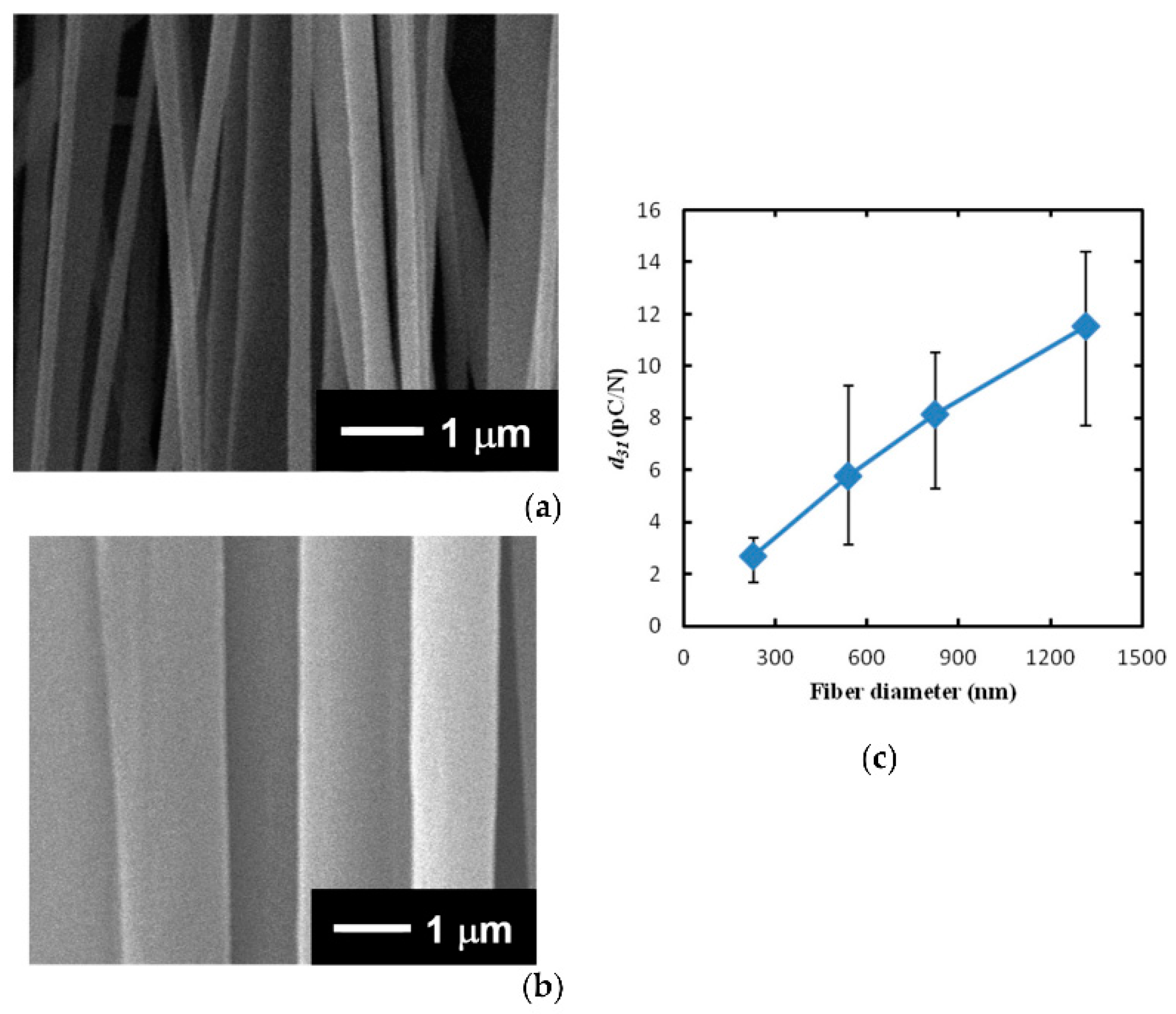
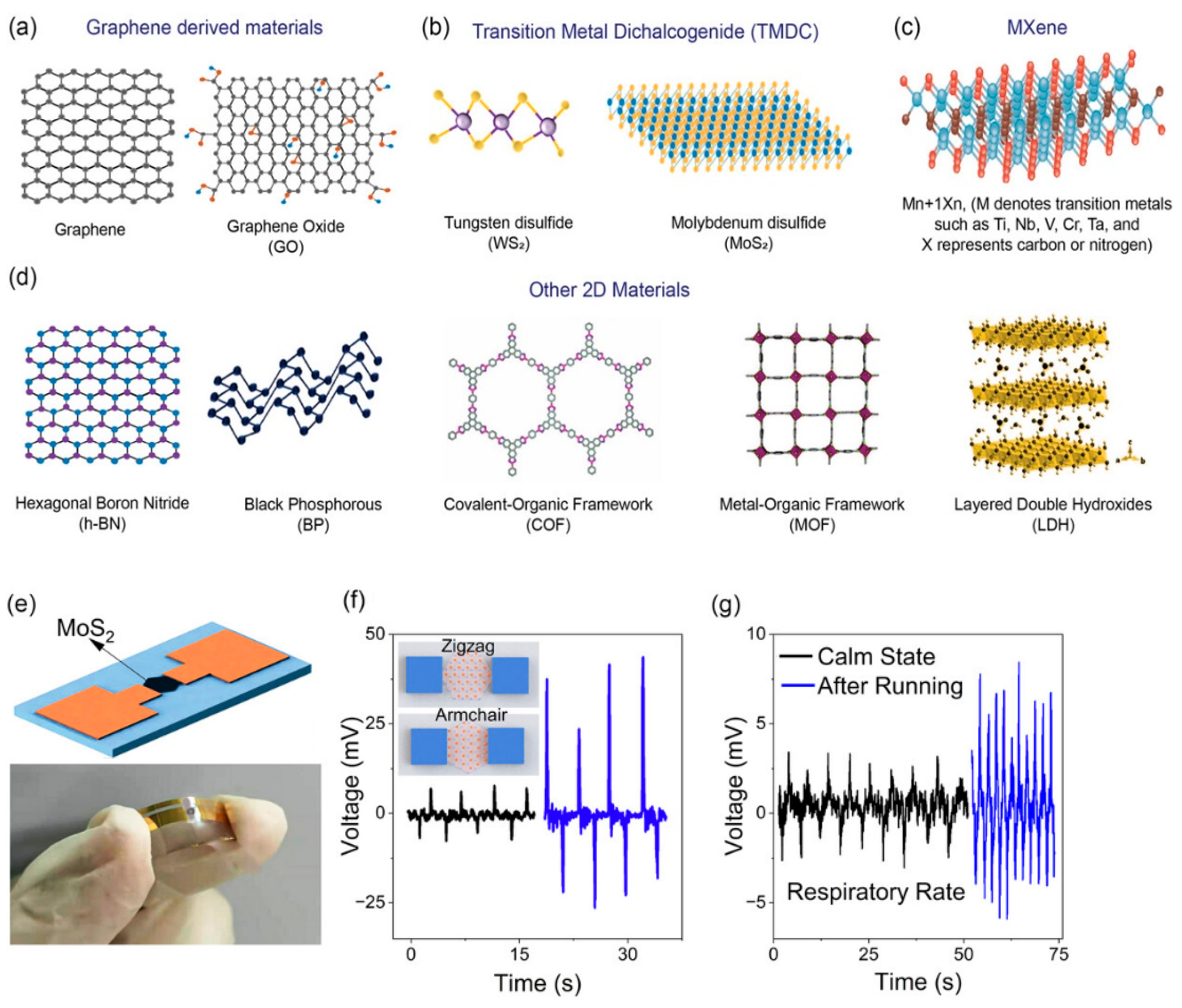
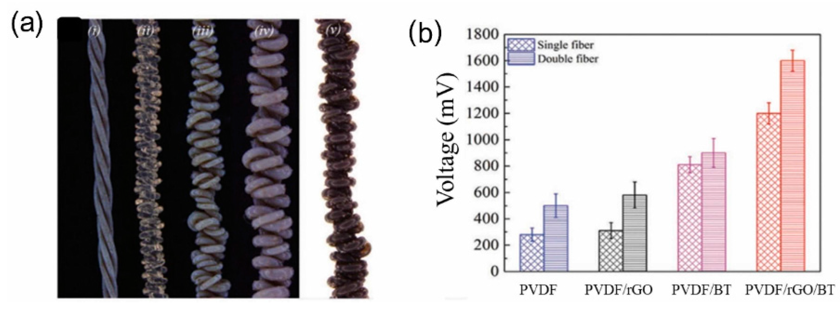
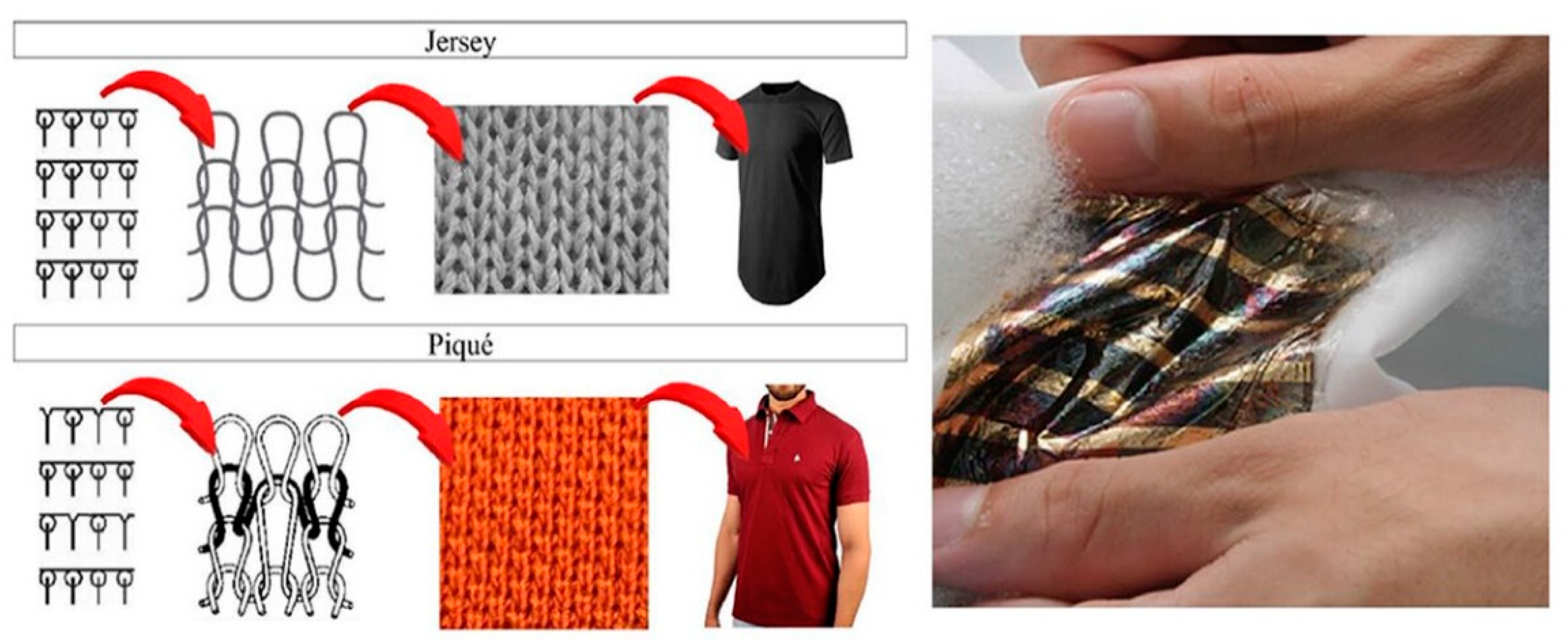
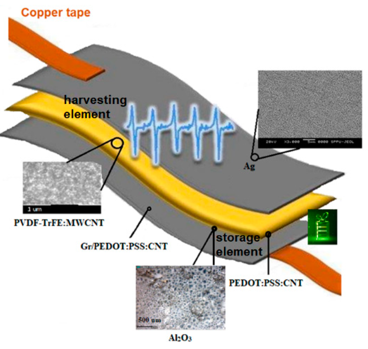
2. Thin-Film Piezoelectric Generators for Wearable Power Supplies

The field of thin-film piezoelectric generators (TFPGs) for wearable power supplies has witnessed significant advancements in recent years, driven by the increasing demand for flexible, lightweight, and efficient energy harvesting systems. These systems are particularly relevant in the context of wearable electronics, where the integration of power sources with minimal bulk and weight is crucial. While the main focus of this paper is on the circuit configurations intended for systems that supply power for wearable devices, this section aims to give a general idea about the structure, materials, and fabrication process of the piezoelectric converting elements, serving as a source of signal for the circuits under consideration. It is based on selected up-to-date literature in the field and presents typical values of the generated power at stereotypical motions, and respective mechanical loads from prototypes that are proven applicable in wearable technology. Recent developments have led to the creation of self-powered wearable devices that can monitor physiological parameters, such as heart rate and motion, without the need for external power sources [52]. The up-to-date values from a single energy harvester, when worn and subjected to ~8 km/h movement, generate ~27 mW. This corresponds to a power density of 0.3 W/kg at an excitation frequency of 3 Hz and is typical for human motion. Experimental results demonstrate the power generation capabilities of sensor wearable devices [53].
Recent studies have focused on various piezoelectric materials, including zinc oxide (ZnO) and lead zirconate titanate (PZT), which are commonly used in TFPGs due to their favorable piezoelectric properties. Although they are well known, the efforts for their enhancement continue. The effects of crystallographic orientation and doping for bulk interfacing on the output current of the easy tunable ZnO thin films reveal that the piezoelectric response diminishes under excessive mechanical stress, which is critical for optimizing device performance under real-world conditions [54]. For example, it was found that the composition of 10 wt% NiO in ZnO yielded 65 V and 4.1 µA under a 30 N load at 4 Hz, which corresponds to a power density of 37.9 µW/cm2. The practical utility of the optimized TFPG has been demonstrated by charging capacitors and powering display devices [55]. PZT thin film and organic P(VDF-TrFE) membrane was fabricated using a straightforward layer-by-layer approach. To achieve flexibility, PZT films were deposited on two-dimensional mica substrates (Figure 1). The resulting composite converts external strain into electrical signals, generating an output voltage of 4 V and a current of 180 nA under 60° bending-releasing cycles, which is applicable for monitoring daily physiological motions.
The flexibility of the substrate plays a crucial role in enhancing the piezoelectric response. Ali et al., noted that ZnO films on flexible PET substrates exhibited superior piezoelectric currents compared to those on rigid glass substrates [56]. Similarly, the deposition conditions and temperature of growth affect polymeric fibers from poly (vinylidene fluoride) (PVDF), resulting in variation in their diameter from 228 nm to 1315 nm (Figure 2) and, respectively, enhanced the piezoelectric coefficient d31 by approximately six times [57].
The incorporation of two-dimensional (2D) materials, such as graphene and transition metal dichalcogenides (Figure 3a–d), has shown promise in improving the piezoelectric properties and flexibility of devices [58]. These materials exhibit high mechanical strength and, in addition, can combine sensing and harvesting functions (Figure 3e–g) [59].
The integration of piezoelectric materials into wearable devices has been facilitated by advancements in nanogenerator technology. Song et al. reviewed the progress in flexible nanogenerators, emphasizing their ability to convert mechanical energy into electrical energy effectively being bio-piezoelectric materials, such as fibrillar proteins (collagen, chitin, and elastin), bioactive polymers, such as poly (lactic acid) (PLLA), poly (lactic acid) γ-Benzylglutamic acid (PBG), and cellulose [60]. This capability is particularly advantageous for self-powered systems, where an implantable continuous energy supply is essential. Some of the reported materials are implemented in structures, exhibiting an output voltage of ~85 V, and a short-circuit current of ~1.6 μA. The power density reaches 4115 μW/cm3 at specific activating conditions.
The integration of piezoelectric materials into textiles has gained attention, allowing for the development of smart fabrics that can harvest energy from everyday movements. Recent studies have focused on weaving piezoelectric fibers into textiles, enabling the creation of wearable energy harvesting systems that are both functional (Figure 4a,b) [61] and esthetically pleasant (Figure 5) [62]. The PVDF/KNN nanocomposite filament-based PENG demonstrated significantly enhanced electrical performance compared to pure PVDF and PVDF/BT counterparts. Under specific loading conditions, the nanocomposite generated a peak voltage of 3.7 V and a current of 0.326 µA, while the pure PVDF filament yielded a peak voltage of only 1.9 V. The incorporation of reduced graphene oxide rGO in PVDF/PU-based PENG exhibited a power density of 66.39 mW/m2 under a constant load and frequency of 3.82 N and 2.5 Hz, respectively. A new functionality such as washing ability is expected from the textile-based piezoelectric thin-film generators. To reduce the effect of the water on the generator’s performance, a piezopolymeric device with plasma treatment has been developed, rendering the surface superhydrophobic and self-cleaning [63]. After immersion in water, an output voltage of 3.50 V, a current of 241 nA, and an increase of approximately 30% in the piezoelectric performance were measured in comparison to that of the untreated surface. These innovations in fabrication techniques are crucial for the commercialization and widespread adoption of thin-film piezoelectric generators in wearable technology.
The fabrication techniques for flexible piezoelectric films have also evolved, with various methods being employed to enhance their performance. Zhen et al. provided a comprehensive overview of fabrication techniques such as sol–gel, hydrothermal, and electrospinning, emphasizing their suitability for producing flexible inorganic piezoelectric films (Figure 6) [65].
This versatility in fabrication allows for the tailoring of material properties to meet specific application requirements. For example, the PMN-PT-based energy harvester can conform to the intricate surface of the heart muscle, generating a substantial 2.7 μJ of power, sufficient to drive a cardiac pacemaker. As per the laser lift-off, under optimal conditions, the device delivered a maximum current of 35 µA and a voltage of 200 V at significant bending. Furthermore, Yeo et al. highlighted the advantages of using PZT films on flexible metal foils, which enable energy harvesting from low-frequency mechanical excitations. This is a common scenario in wearable applications such as wrist-worn devices with a maximum generated power of 201 μW and with a maximum voltage of 1.85 V obtained at a load resistance of 17 kΩ [66]. Recent advancements in electrospinning techniques have enabled the production of nanofibrous piezoelectric membranes that exhibit superior flexibility and high surface area, which are critical for wearable applications [67]. Additionally, the use of 3D printing technologies has facilitated the creation of complex geometries and structures that can optimize the performance of piezoelectric devices [68].
The typical values for piezoelectric elements [54,69,70,71,72,73,74] used in wearable energy harvesters in recent years are presented in Table 1.
PVDF has good strain recovery and can endure cyclic loading, but it may degrade due to UV exposure or moisture over time, necessitating protective coatings. BaTiO3 may be prone to mechanical fragility, and its long-term performance can be affected by thermal cycling and stress fatigue. A composite between PVDF and barium titanate results in maintaining good mechanical flexibility while benefiting from the high piezoelectric activity. Barium titanate can improve the thermal stability of the composite material, allowing it to perform better under varying temperature conditions compared to PVDF alone. It shows relatively good resistance to mechanical fatigue, but its brittleness can be a concern over time in dynamic environments. For wearable applications, it must be combined with a flexible polymer, therefore, PVDF is among the most suitable options. The modified PZT material exhibits enhanced piezoelectric properties combined with improved electric properties due to the incorporation of niobium. This composite provides better mechanical resilience than standard PZT, but is still subject to fatigue under repeated stress, and for this reason it is preferred for transducers not requiring multiple bending conditions. The incorporation of copper complexes in PVDF enhances the conductivity, but the long-term stability against moisture and oxidation is also a consideration. Such a composite is useful in smart textiles where conductive properties are beneficial, but care must be taken regarding material stability, especially when washing. NiO:ZnO has relatively strong piezoelectric properties and is known for good electrochemical stability. PZT has excellent energy conversion efficiency, it is relatively brittle and can suffer from fatigue with prolonged mechanical cycling. PVDF-TrFE is a copolymer, which enhances the piezoelectric effects of PVDF with improved mechanical properties and sensitivity. Regarding its long-term stability, it is superior to PVDF.
Most researchers have focused on using electrospinning and spin-coating for fabrication of the piezoelectric coatings, as can be seen from Table 1. Electrospinning involves drawing a polymer solution (e.g., PVDF) through a charged needle, producing fine fibers. The fibrous structure can improve the mechanical flexibility and toughness of the composite. Spin coating involves depositing a liquid solution of the composite onto a substrate, which is then rapidly spun to spread the liquid evenly, forming a thin film as the solvent evaporates. The process is relatively simple, making it suitable for large-scale production and integration into the existing manufacturing processes. The resulting films have excellent surface smoothness, which is beneficial for applications requiring precise contact between layers (e.g., in multilayer devices). Electrospinning can be more complex and may require more optimization to control fiber diameter and uniformity.
Once fabricated, the piezoelectric element has to be connected with the processing circuit. Power management systems can regulate the flow of energy between the PENGs and storage devices, ensuring that energy is efficiently captured, stored, and utilized. Details related to these systems will be discussed in the next sections of the paper.

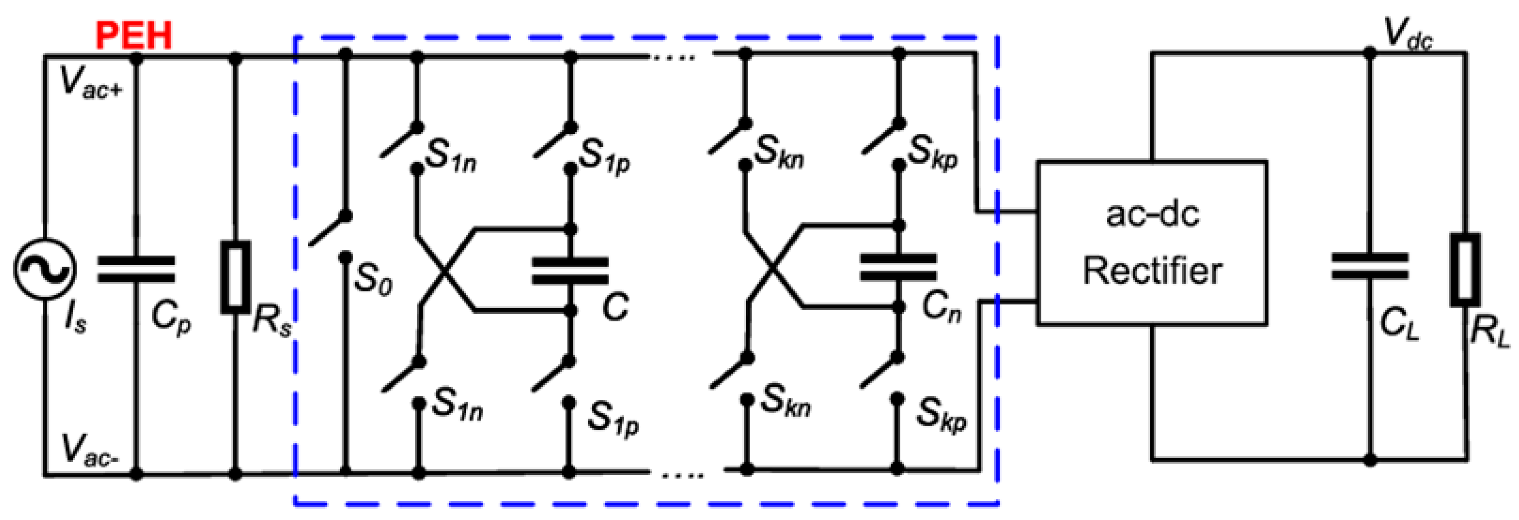
3. Multiplayer Supercapacitors, Designed for Piezoelectric Energy Harvesters

The intermittent nature of piezoelectric energy generation often leads to energy loss during periods of low mechanical input. By incorporating thin supercapacitors, the energy generated can be stored and utilized during these low-input periods, thus reducing energy loss. This capability is particularly beneficial in wearable applications, where energy demands can fluctuate significantly. By providing a buffer for energy fluctuations, these systems can maintain a consistent power output (Figure 7), which is essential for applications in health monitoring and other critical areas [75]. Thin supercapacitors have emerged as a promising technology for this purpose, offering the advantages of high power density, rapid charge–discharge capabilities, and long life [76]. This section will explore the latest studies on thin supercapacitors, emphasizing their integration with piezoelectric generators to create efficient energy harvesting systems with reduced energy loss and enhanced system reliability. Recent research has focused on developing thin supercapacitors that are lightweight and flexible, because these advancements are crucial for wearable devices and portable electronics, where space and weight constraints are of the greatest importance.
The alternate periodic nature of energy generation from PENGs necessitates the incorporation of efficient energy storage solutions to ensure a stable power supply for wearable devices. Supercapacitors have emerged as a promising energy storage solution for wearable applications due to their high power density, rapid charging capabilities, and long life cycle [77]. Recent advancements in flexible supercapacitor technologies have focused on developing lightweight and conformable devices that can be easily integrated with PENGs. For instance, the use of novel materials such as MXene and graphene in supercapacitor electrodes has led to significant improvements in energy storage performance, making them suitable for wearable applications [78]. These materials not only enhance the electrochemical performance of supercapacitors but also provide the necessary flexibility and durability required for integration with wearable devices. Shimada et al. demonstrated a correlation between the inserted in MXene elements with specific atomic number and their effect on the double-layer capacitance, which can explain the superior storage performance of these devices [79]. Additives like cobalt are also favorable for the supercapacitor electrochemical performance by synthesizing a composite (Co-MXene) (Figure 8) [80]. The results show that Co-MXene exhibits higher specific capacitance (up to 1200 F/g vs. 300 F/g for pristine MXene) and better rate capability. This is due to the synergistic effect between the high conductivity of MXene and the redox activity of cobalt.
The choice of materials is critical in enhancing the performance of thin supercapacitors. The researchers have explored various electrode materials, including carbon-based materials, conducting polymers, and transition metal oxides due to their high surface areas and conductivity, which facilitate efficient ion transport and charge accumulation (Figure 9). For instance, in [81] it has been demonstrated that using graphene oxide as an electrode material significantly improved the specific capacitance and energy density of the supercapacitor. Additionally, hybrid materials (MXenes) and those combining conducting polymers with carbon nanotubes have shown promise in achieving higher capacitance values while maintaining flexibility [82,83].
Innovative designs have also contributed to the advancement of thin supercapacitors. Researchers have developed novel architectures, such as 3D porous structures, which further enhanced the surface area available for charge storage (Figure 10).
Some authors have reported a 3D printed supercapacitor design that achieved a specific capacitance of 1.48 F/cm2 while remaining lightweight, flexible, and relatively stable after 500 charge–discharge cycles [86]. Furthermore, the integration of supercapacitors with piezoelectric generators has been explored to create joint self-sustaining energy systems on the same flexible substrate without external connection (Figure 11). This integration allows for the efficient storage of energy generated during mechanical vibrations with direct electrical transfer, thereby enhancing the overall energy efficiency of the system [87].
Repeated deformation can cause fatigue in the electrode materials, leading to cracking, delamination, and reduced performance over time. The choice of substrate, electrode materials (e.g., their flexibility, conductivity, and adherence to the substrate), and packaging is critical in mitigating these issues. Research is currently focused on more robust materials and designs that withstand mechanical stress. A broadly accepted approach is nanostructuring and nanocoposite formations with elastic polymers such as polyurethane to enhance flexibility. Adding crosslinking agents where possible also improves the mechanical stability of the polymer chains. Graphene and other carbon-based materials are often hybridized with other 2D materials like MXenes. Three-dimensional architectures, such as those using porous scaffolds or interconnected networks of nanomaterials, offer superior flexibility and mechanical resilience. Details about the approach toward achieving long-term stability at bending and improve the applicability in wearable devices can be found in [85,89,90]. The substrate must be flexible, durable, and provide good adhesion for the electrode materials. Mismatch in thermal expansion coefficients between the substrate and electrodes can lead to delamination. Polyimide (PI) offers excellent flexibility and thermal stability, but can be expensive, while polyethylene terephthalate (PET) is cost-effective and flexible, but exhibits limited thermal stability. Therefore, suitable alternatives are be elastomers (e.g., polydimethylsiloxane (PDMS)), which are stretchable and preferable for applications requiring significant deformation. In addition, this solves the problem of protecting the device from environmental factors (moisture, oxygen) and mechanical damage, because it must also be biocompatible for wearable applications [91,92].
Exposure to sweat, moisture, and other bodily fluids presents a significant challenge. Electrolytes can be affected by the chemical composition of these fluids, altering their performance. Moreover, these factors can increase the corrosion of electrodes and reduce the lifespan of the device. Encapsulation and the use of protective coatings are essential to safeguard supercapacitors. Hermetic sealing within a polymer film, embedding in a flexible polymer matrix, and incorporating protective layers, are among the approaches to mitigate this effect. For example, conformal coatings using parylene or epoxy resins are commonly used to create a barrier against moisture and chemicals [93,94].
The performance of thin supercapacitors is typically evaluated based on specific capacitance, energy density, power density, and cycle stability. Recent studies [90,95,96,97,98,99] have reported significant improvements in these metrics (Table 2). For example, Swain et al. [90] have developed a thin supercapacitor that exhibited high gravimetric capacitance of 150 F/g, an energy density of 49.8 Wh/kg, and excellent cycle stability of 70% over 10,000 cycles. These advancements are crucial for applications requiring reliable and long-lasting energy storage solutions.

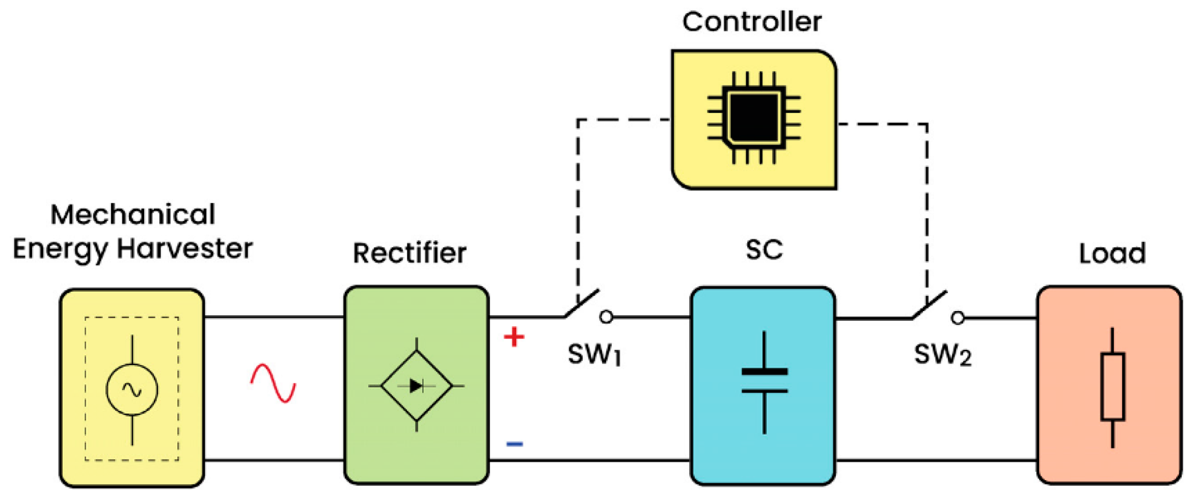
4. Electronic Circuits Used to Convert AC to DC Voltage

4.1. Circuit Configurations with Discrete Components

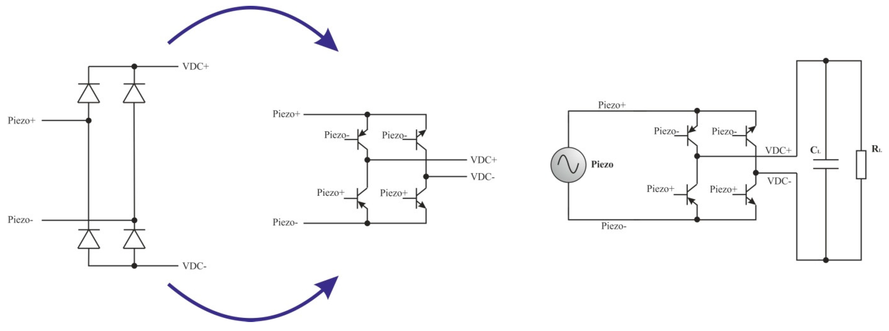
4.1.1. Standard Diode Bridge Rectifier

To build the power supplies for wearable electronic modules and systems, as shown in Figure 7, it is necessary to convert the AC voltage produced by the piezoelectric generator (or piezo harvesters) into a DC voltage using a rectifier and then use a DC-DC regulator to obtain a stabilized voltage. In this case, the collected electrical energy has to be transferred to supercapacitors to ensure the continuous operation of the powered wearable devices. As shown in Figure 7, two DC-DC converters are most often used, and they are generally connected in cascade before and after the energy storage elements. In this way, when there are periods of low physical activity in the patients, the supercapacitors can provide a supply voltage in the discharge mode of operation.
The basic electronic circuit used to convert AC voltage generated from piezoelectric elements to DC voltage is the standard diode bridge rectifier [100,101,102]. In fact, this bridge rectifier is used as a basic circuit configuration that has found extensive application in many interface circuits that convert electrical energy from various thin-film piezoelectric or triboelectric generators. This rectifier is used as a basic configuration against which all other rectifiers, which have multiple improvements, are compared. An electronic circuit of a diode bridge rectifier with a connected source of an input signal, for example, a piezoelectric generator (represented as an ideal current source and in parallel with it a parasitic capacitance Co) and a connected external load with an impedance determined by RL and CL is shown in Figure 12a. The capacitance CL is assumed to be large enough so that the output voltage is essentially constant. To illustrate the principle of operation in Figure 12b, time diagrams are given including the current ip with approximately sinusoidal waveform, the voltage drops vp across the capacitance Cp, and the current io through the external load. For this analysis, it is assumed that the internal parasitic resistance rp is of sufficiently large value (or rp → ∞) and can be neglected. During the time interval from the initial moment to t1, the capacity Cp is charged. In this time interval, all diodes are reverse-biased, and no current flows to the output of the circuit. This process continues until the voltage reaches a value:
V p , m = V R E C T + 2 V D ,
where V R E C T is the output rectified voltage and 2 V D is twice the value of the diode forward voltages.
During the time interval from t1 to t2, current flows to the output network. Therefore, at internal resistance rp → ∞, it can be written as [101]
i o ( t ) = { 0 , a t 0 ω t ω t 1 C L C L + C P | I P sin ω t | , a t ω t 1 ω t ω t 2 ,
where ω t 2 = π and ω is the frequency of the mechanical vibrations.
Assuming that CL >> CP, most of the generated current will flow to the output of the circuit. In this case, the parasitic capacitance of the CP will be a smaller value. Then, we can obtain
C L C L + C P I P I P .
For the average value of the output current at C L > > C P , R L and rp → ∞, we obtain
I o = 1 π ω t 1 π I P sin ω t d ω t = 1 π I P + 1 π I P cos ω t 1 .
To determine the component cos ω t 1 , the formula for the rectified voltage V R E C T is used, according to the following [100,101,102]
v p ( t 1 ) = V R E C T = 1 ω C P 0 ω t 1 I P sin ( ω t ) d ω t + v p ( 0 ) 0 = 1 ω C P I P ( 1 cos ω t 1 ) .
When solving expression (5) with respect to cos ω t 1 we find
cos ω t 1 = 1 V R E C T ω C P I P .
After substituting Formula (6) into the analytical expression (4) for the output current, we obtain
I o = 2 π I P 1 π V R E C T ω C P .
According to Formula (7), with a larger value of the inter-electrode capacitance of the piezoelectric element, a smaller average value of the output current is obtained, and hence, a smaller value for the power.
The average value of the electrical power that is obtained from the piezoelectric generator under a no-load condition yields
P a v = 1 T 0 T V R E C T i o ( t ) d t = 1 2 π V R E C T ω t 1 π I P sin ω t d ω t ,
where it is substituted d t = d ω t ω and T = 2 π ω .
Then, for the power the following expression is obtained
P a v = 1 2 π ( 2 I P V R E C T V R E C T 2 ω C P ) .
The maximum value of the extracted average power is obtained by equating the first derivative of the power expression to zero (or d P a v d V R E C T = 0 ), at which we find V R E C T = I P ω C P , then
P a v , max = 1 2 π V R E C T 2 ω C P .
If r p , the output voltage decreases. To determine the output voltage decreases due to the load, the capacitance of the capacitor CL is initially assumed to be infinitely large. Then, the output rectified voltage has a constant value, which is defined as V R E C T . When reducing the resistance RL, i.e., when the load increases, the time to recharge the capacitor CL increases. A steady state is reached when the input charge on the capacitor is equal to the output charge, then the output voltage can be written as [103]
V R E C T = V R E C T ( 1 r p 2 R L ) ,
where R L = V R E C T / I L is the load resistance.
Then, for the output current, the following expression is obtained [103]
I o = V R E C T 2 r p R L .
As can be seen, the output current depends on the internal resistance rp, and it is desirable to have a relatively small value. This means that the conductive electrodes located on the outer sides of the thin film energy harvesting generators must have the lowest resistance possible, otherwise the output current can be limited.
From a practical point of view, it is essential to determine the output current IL through the external load RL, because based on IL, the power delivered to the load and the electrical energy efficiency of the rectifier can be determined. In the condition that an external resistance RL is included in the output port of the rectifier and the grounded capacitor CL is initially assumed to be infinitely large, according to [93] the IL can be determined from the following analytical expression:
I L = 2 π I P 4 π V D ω C P 1 + 2 π V R E C T ω C P R L .
Then, according to [104], the output power (taking into account the power dissipation PD of the diodes) is obtained as
P o u t = I L 2 R L P L + 2 V D I L P D = ( 2 π I P 4 π V D ω C P 1 + 2 π V R E C T ω C P R L ) 2 R L + 2 V D ( 2 π I P 4 π V D ω C P 1 + 2 π V R E C T ω C P R L ) .
Based on an analysis of Formula (14), the maximum value of the load power PL can be obtained by differentiating the analytical expression concerning the resistance RL and equalizing it to zero or d P L d R L = 0 . For the optimal value of resistance, RL is found
R L , o p t = π 2 × 1 ω C p ( 1 + 2 V D V L ) .
Then, in case the parasitic capacitance Cp can be neglected, the maximum value of the power is obtained as
P L , max = ( 2 π I P ) 2 R L .
According to Formula (16), it follows that greater output power can be obtained with a greater polarization current Ip and a smaller value of the voltage drop VD on the rectifier diodes.
The analysis of Formula (16) shows that the optimal value of the resistance RL depends on the voltage drop across the diodes, the angular frequency ω of the current source ip, and the parasitic capacitance Cp. With a small value of the capacitance Cp, a larger value of the output voltage can be obtained. Also, with a small value of the voltage VD, the output voltage will be larger. In terms of the value of the angular frequency, a higher current and correspondingly higher power are obtained when the piezoelectric element reaches resonance. In this case, an optimal load is determined for a given frequency.
A superposed ripple voltage occurs over the load for a finite value of the output filter capacitor CL. The peak-to-peak pulsating voltage swing is calculated from the charge delivered by the capacitor during the discharge time td [103] using the following:
V L , p p = I L t d C L = π I L ω C L ( 1 r p 2 R L 4 ) ,
where t d = π ω ( 1 r p 2 R L 4 ) is the time interval determined by the frequency of the mechanical vibrations.
Then, based on Formula (16), an appropriate value of the capacity of the CL can be found at certain parameters for the energy harvesting generator and the external load [103]:
C L = π I L ω V L , p p ( 1 r p 2 R L 4 ) .
The following approximate relationship for voltages can be used to determine the voltage [92] V L , p p : V L , p p 3 2 ( V R E C T V L , min ) , where V L , min is the minimum value of the output voltage for a specified load RL.
The analysis of Formulas (5) and (7) shows that the average value of the output current and the value of the rectified voltage depend on the polarization current IP, which is generated by the piezoelectric element. In this case, the change in the frequency of the mechanical vibrations leads to a change in the current IP, and hence to a change in the values of the quantities in the output network. Also, as can be seen from Formulas (11) and (12), changing the parameters of the external load reduces the value of the rectified voltage and current. One possible way to reduce the variations in the output voltage is to connect a capacitor CL in parallel to the output. In this case, the output voltage is smoothed, reducing the ripple. However, to a large extent, energy harvesting generators are unstable, resulting in variations in output voltage and current. Simultaneously, all electronic signal processing circuits for wearable electronic devices require stable values for the supply voltage and current. This requires energy storage elements such as electrolytic capacitors, supercapacitors (formerly called ultra-capacitors), and even in some cases miniature rechargeable batteries to be added to the energy harvesting and conversion circuits.
In order to facilitate the achievement of the optimum voltage at the output of the rectifier, a low-power DC-DC converter is most often added, as shown in Figure 13. As can be seen in Figure 13, the low-power DC-DC converter is connected between the rectifier output and the energy storage element. Typically, the internal controller of this type of converter is designed to regulate the output voltage to provide an optimal mode for charging the storage element. It is noteworthy that in several wearable electronic devices, commercially available energy harvesting circuits, such as the example electronic devices in the previous section, are already used as DC-DC converters. For some of them, since the energy obtained from the energy harvesting generators is unstable, it is recommended that the energy storage element be connected immediately after the rectifier. Then, the voltage conversion is carried out, as in their output port small electrolytic capacitors are connected.
The basic electrical parameter that is related to the workability of the DC-DC converters is the overall electrical energy efficiency (or power conversion efficiency), which can be obtained by using the following analytical expression:
η = P o P i n × 100 % ,
where P i n is the input power and P o = V S T O R 2 / R L is the output power of the converter and RL is the external load.
Also, for the AC-DC converter circuits, the efficiency of a certain configuration can be evaluated by the so-called figure of merit or simply FoM. This parameter can be calculated as the ratio of the output power P o that can be delivered from the storage element (rechargeable battery or supercapacitor) to the maximum average power P ^ P E H , max that can be obtained from the piezoelectric element, provided that the lossless rectifier ( V D 0 V ):
F o M = P o P ^ P E H , max = P o C p f V p , max 2 .
A far more optimized solution was presented in the work of Aktakka et al., where the diodes were substituted with a set of NPN and PNP transistors [40]. If these transistors are properly chosen, the power losses over them will be drastically limited ( r c e should be as low as possible). The substitution and resulting change in the base piezoelectric element structure are shown in Figure 14.
To validate the efficiency of such a design solution, we ran a few brief simulations on LTSpice by using SPICE models of existing BJT transistors and Schottky diodes. To perform the simulation study, simulation models of discrete components were used, 2N3904 (ON Semiconductor Corporation, Scottsdale, AZ, USA) was used for NPN transistors, and 2N2905A (STMicroelectronic, Geneva, Switzerland) was used for PNP transistors. PMEG2010AEB (Nexperia, Nijmegen, The Netherlands) was used for the Schottky diodes. The parameters of the load were selected with the following values: R L = 1 kΩ and C L = 10 μF. Figure 15 shows the results from the simulation. It shows that by substituting the Schottky diodes with bipolar transistors a noticeable increase in the rectifier’s output voltage can be observed.
The results from the simulated evaluation of the two circuits show that the addition of a BJT rectifier improves the circuit’s overall performance by decreasing the voltage losses. It can be seen that the Schottky diode rectifier’s output voltage reaches a maximum voltage of around 0.7 V at 1 V sine input, whilst the BJT rectifier reaches an output voltage in the vicinity of 0.95 V.

4.1.2. Voltage Doubler Rectifier

For most thin-film energy harvesters, the generated signal is at a relatively small level (up to about a few hundred mV, obtained through single samples [105,106,107,108,109,110,111]). Therefore, increasing its value is necessary to provide the required voltage for subsequent stages and functional parts of the converters. An optimal electronic circuit for increasing the level of the rectified voltage, in this case, is a voltage doubling rectifier, which contains most frequently two low-power Schottky diodes and two capacitors, one of which C1 is connected in series to the piezoelectric generator, and the other C2, connected in parallel to the load (Figure 16 [112,113]). A higher value for the output voltage level can be obtained by using a rectifier with a quadrupling of the output voltage (voltage quadrupler circuits [112,113]), but in this case, the number of diodes increases, and hence the energy efficiency coefficient decreases.
For the principle of operation of the rectifier during the first half-cycle (or negative half-period), and for the polarity of the voltage outside the brackets, the piezoelectric current passes through the diode D 1 charging the capacitor C 1 to the voltage V C 1 = V p m , 0 . For the first half-cycle, the D 1 is in forward mode of operation. During the second half-cycle (or positive half-period) the input voltage (signs in brackets) reverses polarity. The D 1 is turned off, and the sum of the capacitor voltage and the amplitude of the input voltage is applied to it. During the second half-cycle, the D 2 is turned on and the C 2 is charged, with the capacitor C 1 transferring part of its electrical energy until reaching a voltage equal to the sum of the input voltage and the voltage of C 1 . Then, the voltage drop of the C 2 (at no load (RL → ∞), yields V C 2 = V p m , 0 + V C 1 2 V p m , 0 .
The basic waveforms of the currents and voltages [102], representing the operation of the voltage-doubler rectifier (Figure 16) are given in Figure 17. The output voltage v o is similar to the waveform of the load voltage for the bridge rectifier (Figure 15), as it is observed charging of the capacitor C2 through the input signal, and as a result of this process, the level of the output voltage is slightly greater or slightly less than the average value. For larger values of capacitances (C1 and C2), smaller variations in output voltage are expected, and at higher frequencies of mechanical vibrations, smaller deviations may occur.
Provided that no load RL is connected at the output port of the circuit, the piezoelectric sinusoidal current fully charges the capacitance Cp (starting from zero voltage over the Cp or the initial condition is v p ( 0 ) = 0 ), and the peak no-load voltage is obtained as
v p ( T 2 ) = 1 ω C P 0 π ω I P sin ( ω t ) d ω t + v p ( 0 ) = 0 = 2 I P ω C P = 2 V p , m .
As can be seen from Formula (21), the rectified voltage VRECT has a maximum value equal to 2 V p , m . The value of the rectified voltage changes its value during the process of recharging the capacitor C2. Also, when connecting a load RL to the output, the maximum piezoelectric voltage decreases, according to Formula (11), i.e., v p ( t ) < V R E C T . The instantaneous power extracted from the rectifier, yields P L ( t ) = V R E C T i D 2 ( t ) . The current i D 2 ( t ) has a sinusoidal waveform and can be represented by the following analytical expression I P sin ω t for the interval t 1 < t < T 2 . For the rest of the period, the value of the i D 2 ( t ) is equal to zero. Then, the average value of the extracted energy from the piezoelectric element in the voltage-doubler circuit is determined by the same approach as for the bridge rectifier circuit, according to Formula (8). Based on the analysis of Formula (8), the same expression as Formula (10) is obtained for the maximum value of the average power, but for the value of the rectified voltage, determined by the expression V R E C T = 2 I P ω C P . This means that the powers for both rectifiers in the ideal case (without taking into account, for example, the voltage drops on the diodes) are the same, but with the voltage-doubler circuit, the rectified voltage is of a higher value. Therefore, the voltage-doubler circuit can extract maximum power from the piezoelectric element at a lower current. The extracted power at a lower current results in smaller voltage drops across the diodes and hence less power dissipation. In practice, the typical polarization current for the thin-film energy-harvesting elements is up to a few mA, but the reduction in power dissipation leads to an increase in the energy efficiency of the voltage-doubler, which is essential, especially at low-power electronic devices.
Also, the voltage-doubler rectifiers can be very effective in a piezoelectric supercapacitor structure [37]. From an electrical point of view, the structure of the input signal source is a piezoelectric generator, one terminal of which is connected to one terminal of a thin-film supercapacitor. In this case, a series connection of the two elements is obtained, which allows them to be connected to a voltage-doubler rectifier, as shown in Figure 18. In it, the input signal source is represented as an equivalent current source with an impedance determined by rp and Cp. In the common node of the two elements to limit the voltage over the supercapacitor, several rectifier diodes can be connected to the ground so that the maximum voltage reaches a value up to nVD, where n is the number of the diodes.

4.2. Circuit Configurations with Integrated Components

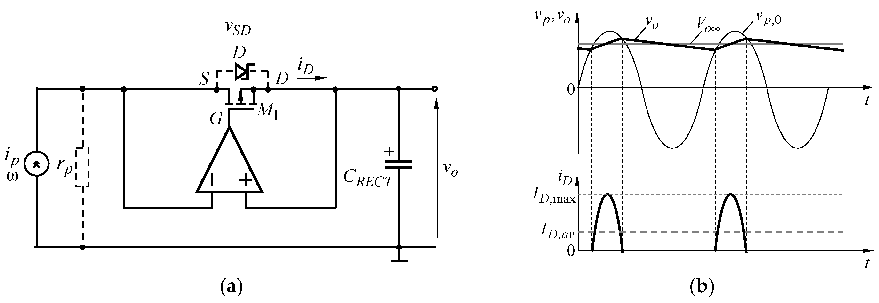
4.2.1. Bridge Rectifier Using MOSFETs

The use of a bridge rectifier with rectifying diodes is simple, but due to the inherent forward voltage drop over them and power loss, it is necessary to consider possible alternatives. A simple solution to mitigate this effect is to use Schottky diodes which have a smaller forward voltage drop, but this does not eliminate the issue. When working with small input voltages generated from thin-film energy harvesters, the diodes in the various types of rectifiers are replaced by bipolar or MOS transistors. This technique is more easily implemented in integrated circuit design. In recent years, MOS transistors (or Metal-Oxide-Semiconductor Field-Effect Transistors (MOSFETs)) have often been used to replace rectifier diodes, since the voltage drop across a single device can be reduced to several tens of millivolts. Thus, the so-called FET diodes are obtained, and both n-channel and n-channel enhancement-type MOS transistors can be used. For the efficient operation of bridge rectifiers with FET diodes, the threshold voltage must have a value no greater than 0.5 V. Such threshold voltage values can be more easily achieved with MOSFETs with a minimum channel length no greater than 100 nm. An example circuit of a bridge rectifier with FET diodes is shown in Figure 19. Two n-channel MOS transistors (M1 and M2) and two n-channel MOS transistors (M3 and M4) are used to build the circuit configuration. To simplify the description of the structure and the principle of operation, the source of the input signal is represented according to Thevenin’s theorem as an ideal voltage source ep and series-connected resistance rp, modeling the internal resistance. The gates of M2 and M3 are connected to node 1, and the gates of M1 and M4 are connected to node 2. At a positive input voltage, transistors M1 and M3 are tuned on and transistors M2 and M4 are turned off. In this case, the voltage VGS1 < 0, and the voltage VGS3 > 0. At the same time, the voltage VGS2 > 0, and the voltage VGS4 < 0. The transistors M1 and M3 are tuned on by operating in a triode mode of operation or with a continuous (non-pinched-off) channel, obtaining an almost straight line of the dependence of iDvDS with a slope proportional to VDSsat. Then, current flows from the source ep through node 1 to the load and then to the common node of the sources of M3 and M4. At a negative input voltage, transistors M1 and M3 are turned off, and transistors M2 and M4 are turned on. In this case, current flows in the same direction through the load. The current flows from the source ep to node 2 and through the load and then to the common node of the sources of M3 and M4, M4 being turned on and M3 being turned off.
At a small value of the voltage VDS, the MOS transistors can be considered as a linear resistance, the value of which can be controlled by the voltage vDSsat. Then, for the drain current of the n-channel MOSFET, the following analytical expression can be written [114]
i D = [ μ n C o x W L ( v G S V t h ) ] v D S ,
where μn is the mobility of the electrons at the surface of the channel, Cox is the total capacitance between gate and channel, W is the width of the channel, L is the length of the channel, and V t h the threshold voltage with typical values in the range of 0.3 V to 1.0 V.
Then, the resistance of the channel when maintaining a small value of v D S is obtained, as follows:
r D S = 1 i D v D S = 1 μ n C o x W L ( v G S V t h ) .
As can be seen from the above expression, the resistance is determined by the following factors: (1) process transconductance parameter k n = μ n C o x [A/V2], (2) the ratio of W / L , and (3) overdrive voltage v D S , max = v G S V t h [V]. The first two factors are largely related to the functional capabilities of the selected microelectronic technology, and the W / L ratio can be changed within certain limits. When defining the W / L ratio, the minimum channel length condition, Lmin, must always be observed. The third parameter is the overdrive voltage v D S , max = v G S V t h , but its value directly determines the magnitude of the electron charge in the channel. For a small value of the voltage v D S the MOS transistor operates as a linear resistance, the value of which is controlled by the voltage v G S = v D S , max n + V t h (where n is the sequence number of a certain value of the overdrive voltage). At v G S V t h the resistance is infinite, and for voltages greater than V t h the resistance decreases.

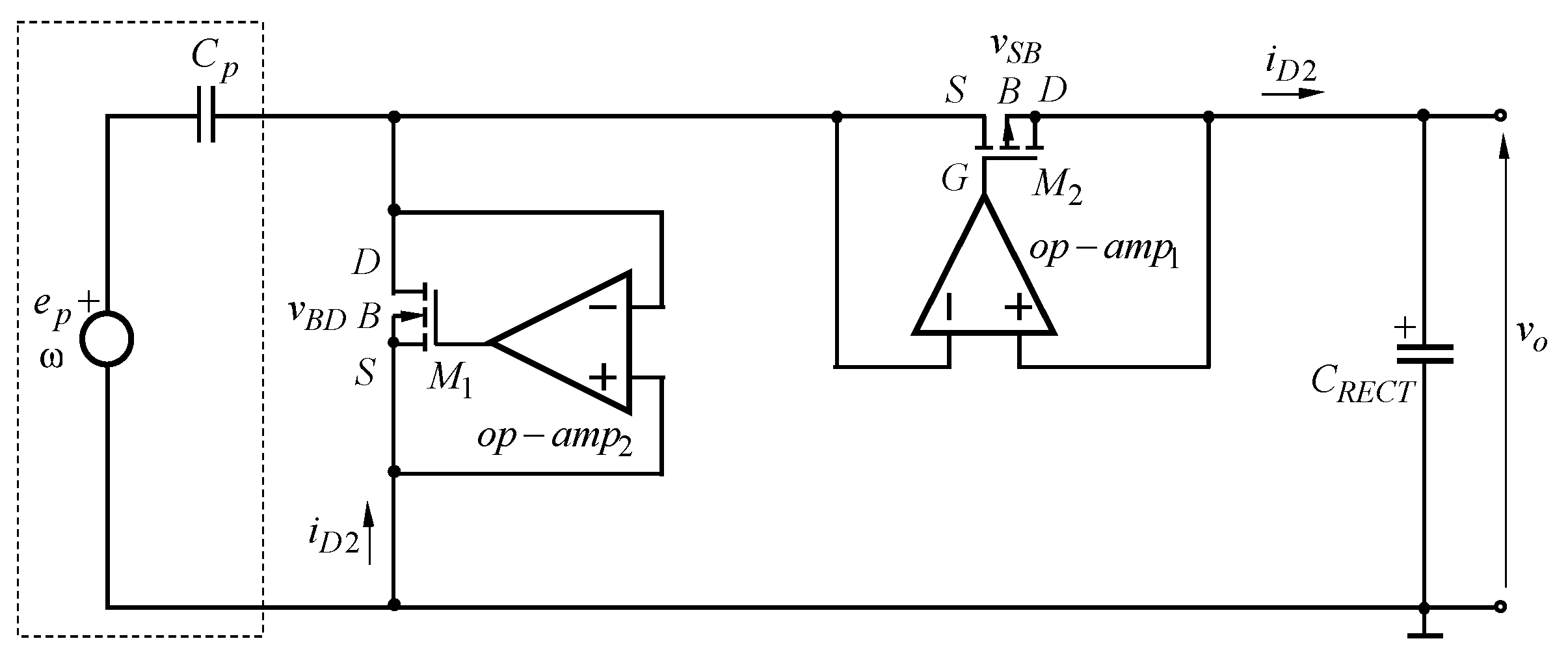
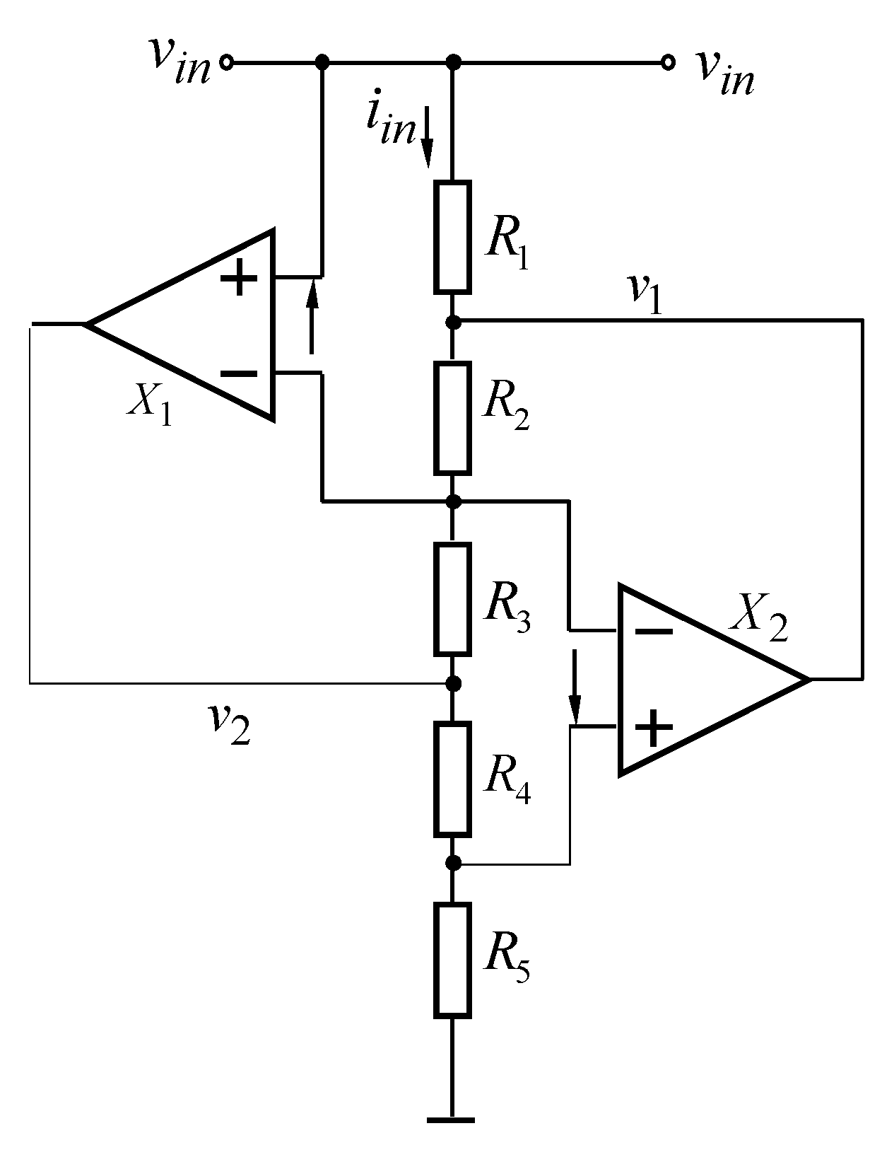
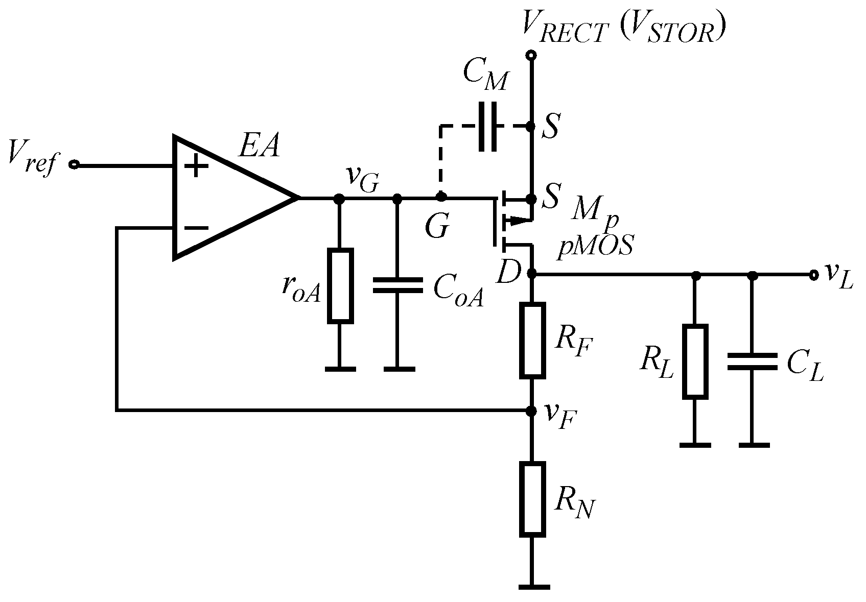
4.2.2. Active Rectifiers

To further limit the voltage drops across the active diodes in the electronic circuits of rectifiers, a modification of the FET diodes can be used, in which the so-called active voltage rectifiers and doublers are obtained [40,115,116]. In this case, the active diode is implemented using a single low-power p-channel MOSFET, controlled by a single operational amplifier (op-amp), whose inverting and non-inverting inputs are connected to source (S) and drain (D), respectively (Figure 20). The gate (G) of the transistor is connected to the output of the op-amp and the bulk (substrate or body) of the transistor is connected to the drain.
For a loop formed by the MOS transistor and the input port of the op-amp according to Kirchhoff Voltage Law (KVL), yields
v i d + v S D V O S = 0 v i d = V O S v S D .
where V O S is the input offset voltage for the chosen op amp; for typical low-power op amps the input offset voltage is up to several mV.
In case the DC differential voltage gain is denoted by Ad, then for the gate voltage of the transistor is obtained, as follows:
v G = A d v i d .
Then, after substituting (24) in Formula (25) for the voltage is found, as follows:
v G = A d ( V O S v S D ) .
As can be seen in Formula (26), since the voltage gain Ad for an ideal amplifier is infinite, small changes in the voltage of vSD will control the gate voltage. Then, provided the amplifier’s inverting input voltage v i is greater than the non-inverting input voltage v i + , the active diode is forward connected (the MOSFET is turned on) and conducts current from source to drain. In case the voltage at the non-inverting input v i + is greater than the voltage at the inverting input v i , the diode is in a reverse circuit (the MOSFET is turned off) and the current can be neglected.
The power supply voltages to forward the active diode are obtained from a supply independent bias circuit. The electrical energy for this circuit is provided by the energy harvesting generator, and its power consumption has to be a small value. This means that the average current should be typically less than 1 μA. In order for the active diode to start working and the operational amplifier to start regulating the voltage drop, the supply voltage must be greater than V t h + 2 V D S s a t [117] or approximately 0.60–0.65 V. To forward the active diode, it is necessary that the voltage between the source and the gate of the MOS transistor becomes less than the threshold voltage VTH, which is with negative polarity. For the short-channel pMOS transistors, the typical value for the threshold voltage is –0.5 V, at VDS = VGS. In this case, if the v i is greater than v i + the voltage at the gate terminal will decrease. This means that the voltage at a source terminal has to be greater than 0.5 V for the transistor to start conducting current so that VGS < −0.5 V. For a higher value of the source voltage, a higher value for the drain current can be obtained.
When the MOS transistor is turned on at small values of the vDS, the channel approximately behaves as a linear resistance (or triode region operation), the value of which is controlled by the vGS, which in turn is determined by the voltage drop vDS, given in [114].
If the effective voltage V D S s a t is of sufficient value, the voltage drop between the source and drain of the transistor is equal to VOS, and then [114]
i D = [ μ n C o x W L ( v G S V t h ) ] V O S .
In the active diode configuration proposed for use, an additional Schottky diode is connected (presented with a dashed line) between S and D of the transistor [41], which provides current for charging the energy storage element until the |VGS| voltage becomes greater than the threshold voltage. In this way, the connection of a relatively complex start-up circuit [118] can be avoided. An example circuit of an active rectifier is given in Figure 21a. In it, the active diode is connected in series with the input signal, and the capacitor CRECT is connected to the equivalent anode and ground of the circuit.
Compared to the rectifiers using rectified diodes in the circuit of the low-power active rectifier (Figure 21a), the voltage drop on the FET diode is a few tenths of millivolts. In the electronic circuit, the active diode is turned on when the voltage vp is higher than the voltage vo, blocking the flow of reverse current when the voltage vp falls below vo. To reduce the value of the reverse current, the bulk of the p-channel MOSFET is always connected to the highest potential available from its source and the drain nodes. In this way, a bulk-regulated MOS transistor structure is obtained [118,119].
If the electrical equivalent circuit of the input source is introduced according to Thevenin’s theorem, then an ideal voltage source e p with internal resistance is obtained r p . To illustrate the principle of operation of the electronic circuit in Figure 21b are given, the time diagrams of the voltage and current through the MOS transistor. In the time interval when the input voltage is greater than the output voltage vo, a current iD flows, and the capacitor CRECT is recharged to a voltage value of V o m , 0 = V p m , 0 V S D . When an external load RL is connected to the output of the circuit, in parallel with the capacitor CRECT, the voltage on the capacitor decreases faster, because the capacitor is discharged through the load. In the time intervals when the MOSFET is turned off, as shown in Figure 21b, the capacitor discharges and reduces the output voltage level. When the MOS transistor is turned on, the capacitor is charged to the maximum value. When the voltage on the capacitor is equal to the current value of the input voltage, the MOS transistor is turned off. The average value of the rectified voltage is determined by Formula (11). Then, for the peak value of the current through the FET diode, we obtain I D , max = V o m , 0 r p R L . Based on the value of the output voltage for the average output current is I L , a v = V o m , / R L , then for the relation between the I L , a v and the repetitive value of the peak current through the diode is δ I L = I L , a v I D , max = ( 1 r p R L ) r p R L . As can be seen, the average value I L , a v is relatively small and depends on the internal resistance of the input source and the resistance of the external load.
The minimum supply voltage for this type of active rectifier is determined by the operational amplifier’s (op-amp) minimum supply voltage and the MOS transistor’s threshold voltage. The supply voltage must be greater than the op-amp’s minimum operating voltage and the MOS transistor’s threshold voltage to ensure proper operation. For the maximum values of the power supply voltage, the same limitation is applied. This voltage should be less than the op-amp’s maximum operating voltage and the MOS transistor’s maximum gate voltage.

4.2.3. Voltage Doubler AC-DC Converters

If the input voltage is not of sufficient amplitude, based on the circuit in Figure 21 and the voltage doubler with Schottky diodes given in Figure 18, the circuit diagram of the voltage doubler AC-DC converter (Figure 22) using two op-amps, which drives the MOSFETs is obtained.
For the electronic circuit in Figure 22, the M1 is an n-channel MOS transistor and the M2 is a p-channel MOS transistor. For transistor M1, the substrate is short-circuited to the source, as for the equivalent diode, the anode matches the substrate and the cathode matches the drain, thus forming a PN junction. For transistor M2, the substrate is short-circuited to the drain, and in this case for the equivalent diode, the anode matches the source and the cathode matches the substrate. The active components in this circuit configuration are the operational amplifiers op-amp1 and op-amp2, which control the operation of the MOSFETs. In some cases, op-amps can be replaced with analog comparators, which allows for faster switching at higher input signal frequencies. The power supply voltage for the operational amplifiers used in the circuit is provided by the output voltage, which is stored on the capacitor CRECT. For the selected connection method, the operational amplifiers measure the voltage between the drain and source of the MOSFETs, forming a control voltage for the gates. Then, the transistors turn on or off depending on the polarity of the voltage between the drain and the source of the transistors. In this way, a controllable resistance is obtained, depending on the polarity of the voltage applied between the two terminals. Specifically, the op-amp1 monitors the voltage between the substrate and the drain of the M1, turning on the transistor when the difference VBD is positive. This occurs when the negative piezoelectric current passes through the diode charging the capacitor C p to the amplitude V C p = V p m , 0 . The op-amp2 monitors the voltage between the source and the substrate of M2, turning on the transistor when the voltage is positive. This occurs when the input voltage becomes higher than the output voltage or the voltage drops over the capacitor CRECT.
If the voltage on the CRECT is insufficient to provide a supply voltage for the operational amplifiers, the charging current is provided by the well-source diodes of the MOSFETs. This most often occurs when mechanical vibrations initially occur, and polarization current is generated.
In order to take into consideration the necessary input voltage for the PEH to operate, it is important to consider which are the limiting factors for it. Voltage drops are present overall active components, with their limitation being of the most importance. Diode voltage drops are present in the rectification circuits, and these voltage drops can be reduced from 0.6 V to 0.2 V if a migration towards Schottky diodes is performed. An additional issue is that these voltage drops roughly increase proportionally to output current consumption due to the diode’s internal resistance. To reduce the losses in the diodes, it is better to implement a rectification circuit using transistors. There are two possible solutions: a MOS rectifier and a BJT rectifier. Our analysis shows that due to the necessity that the U G S voltage must exceed the U T H voltage for all MOS transistors in order to turn them on, in a MOS rectifier, the input voltage has to be sufficiently higher that 2x U T H in order for the circuit to operate linearly and with minimum losses. It is difficult to manufacture MOS transistors with a threshold voltage below 0.5–0.7 V for discrete components, hence necessitating a high input voltage for the PEH of above 1 V. When constructing a BJT rectifier there is a similar issue in that for a bipolar transistor to operate a base-emitter voltage of 0.6–0.7 V needs to be provided, hence requiring the piezo transducer to generate a voltage of above 1.2 V. When implementing circuits which include an operational amplifier or comparator, efforts need to be directed towards choosing low-voltage power supplied ICs. For this the folded cascade configurations are optimal but in practicality, available operational amplifier ICs with a supply voltage of below 1.5–1.8 V are difficult to find and expensive. As a conclusion over this brief discussion, taking under consideration all factors: (1) if the piezo transducer is capable of providing a voltage of below 1 V, then a suitable circuit would implement a Schottky diode rectifier and passive (transformer or resonant-based circuit) voltage boosting prior to further energy-conversion steps; (2) if the piezo transducer can provide more than 1.5 V, then active transistor rectifiers and op-amp circuits can be implemented and utilized.

4.3. Parameter Study for Different Rectifier Stages Topologies of Reported Piezoelectric Energy Harvesting Systems

Ensuring efficient AC-to-DC conversion is one of the key aspects when designing piezoelectric energy harvesting devices. A short comparative study of several carefully selected representative topologies of rectifier stages is presented below, focusing on their primary parameters, performance metrics, and potential applications. A summary of their main parameters is shown in Table 3.
Godinho, A. et al. [120] report an active CMOS rectifier designed in 130 nm CMOS technology which achieves a voltage conversion efficiency (VCE) of 99% and a power conversion efficiency (PCE) of 80% to 90% for input voltages ranging from 0.45 V to 1 V at 3.2 kHz. This circuit employs a threshold cancelation technique and a no-delay comparator to minimize power losses and avoid reverse leakage currents. These features make the rectifier highly suitable for integration into power management circuits (PMCs) for environmental monitoring in wireless sensor networks (WSNs). A voltage flip enhancement concept, using the Fully Autonomous Rectifier (FAR) principle, is analyzed by Frick, V. et al. [121]. The FAR achieves significant power performance improvements for piezoelectric energy harvesting (PEH) systems, especially under high load constraints. The CMOS prototype confirmed robust operation under circuit non-idealities. This solution is well-suited for low-voltage applications, and can be integrated into more complex PEH architectures like SSHI or SSHC for additional performance boosts. Edla, M. et al. [122] introduce an H-Bridge rectifier circuit that demonstrates superior performance over conventional full-bridge rectifiers (FBRs) in low-frequency, human-induced motion scenarios. Their experimental results indicate that the H-Bridge produces a maximum rectified voltage of 3.8 V DC and 21.05 μW of output power during walking tests, outperforming the FBR circuit’s 1.6 V DC and 5.01 μW. The circuit also offers higher stability, making it a suitable choice for wearable energy harvesting devices. Further investigation into dual-stage H-Bridge circuits is recommended for extended applications. A dual-output piezoelectric rectifier implemented in 65 nm CMOS technology, developed by Yuen, P. W. et al. [123], addresses the limitations of conventional rectifiers. The proposed NMOS rectifier achieves a VCE of over 98% and a peak PCE of 84%, delivering 120 mW of output power with a load resistance of 12 kΩ. The circuit covers an active area of 0.00372 mm2 and provides a rectified voltage of 1.21 V with a current of 101.12 mA. This design is highly effective for low-power WSN devices. The Voltage Doubler Joule Thief (VDJT) circuit presented by Kamran, M. et al. [124], integrates voltage doubler and joule thief principles to optimize AC-DC conversion. Laboratory tests validated the VDJT circuit, achieving an efficiency of 72.3% by converting an input of 15 V AC at 5 Hz to an output of 18 V DC and 5500 μW of power. Its compact design makes it suitable for miniaturized energy harvesting systems. However, further exploration of control methodologies for boosting voltage is needed.

5. SSHI (Synchronized Switch Harvesting on Inductor) Based Energy Harvesting Circuits

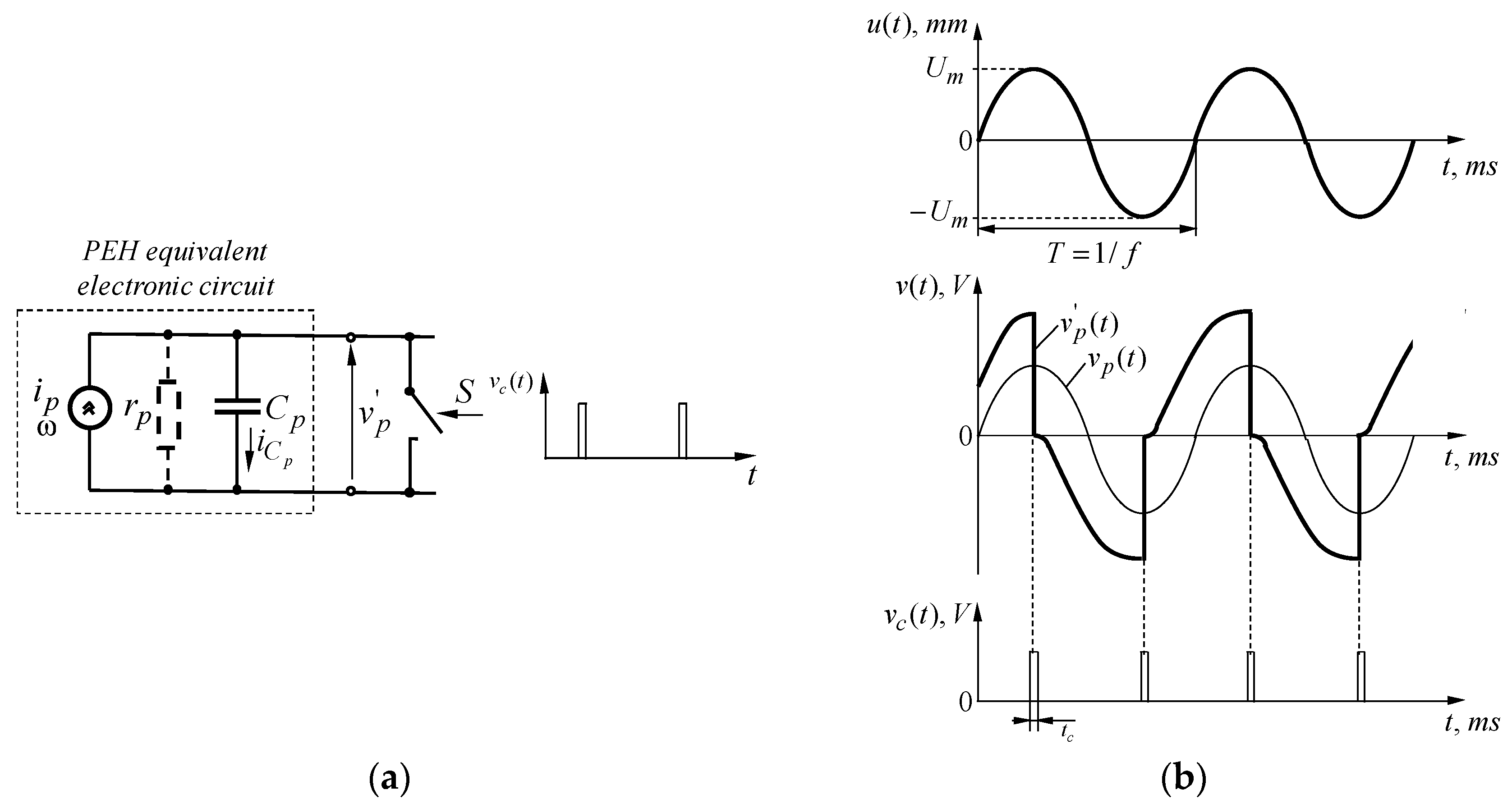
5.1. General Principle of a SSHI Technique

The use of bridge rectifiers or voltage multiplier rectifiers makes it possible to directly convert the polarization voltage caused by mechanical vibrations. The main drawback of this method is the presence of voltage drops across the rectifier components, which can significantly reduce the harvested electrical energy, especially at generated low voltages. Also, during the change in polarity of the piezoelectric current, the stored charge on the internal capacitor of the transducer is wasted, which further reduces the efficiency of operation [125,126,127,128,129,130]. One of the widely used and interesting methods for extracting more electrical energy for wearable power supplies is by building bias-flip input stages [125,126,127,128,129,130] in which the amplitude of the AC voltage is increased up to two times. Moreover, this type of bias-flip input stage is connected before the voltage rectifier. Thus, the harvesting efficiency obtained by the piezoelectric generator can be increased. Specifically, Figure 23a shows a functional circuit of an input stage with an additional electronic switch connected in parallel to the piezoelectric element. For the piezoelectric element in a steady state, a sinusoidal excitation u ( t ) = U m sin ω t is applied, where U m is the maximum deflection and ω is the angular frequency of the vibrations. In the operation of the piezoelectric element, it is assumed that the produced periodic signal v p ( t ) is symmetrical according to the x-axis, and has a sinusoidal waveform and a frequency determined by the mechanical vibrations on the cantilever. When the input signal reaches its amplitude, the electronic switch S closes under the action of a control pulse v c ( t ) and the voltage v p ( t ) becomes equal to zero. The time interval tp during which the switch is closed must be no more than 1/100 of the period of the input signal. After the time interval of the control pulse has expired, the voltage v p ( t ) starts to change from zero depending on the instantaneous value of the v p ( t ) . This change continues until the input signal again reaches an amplitude value with negative polarity. The switch then closes again for a short time tc. The signal v p ( t ) becomes equal to zero and after opening the switch the signal starts to change depending on the current value of v p ( t ) . The process is then repeated, and as shown in Figure 23b, the voltage v p ( t ) reaches an amplitude (at no load operation) up to twice the value of the amplitude of the v p ( t ) . As can be seen, in Figure 23b, the voltage v p ( t ) is phase-shifted and has a waveform different than a sinusoidal signal. Also, for the proper operation, it is necessary that the control signal is synchronized with the input signal v p ( t ) and has a frequency twice that of v p ( t ) . The control pulse is generated by an electronic circuit with power supplied from the energy storage element included in the output port for the wearable power supply. Thus, a “self-powered” electronic switch is obtained.

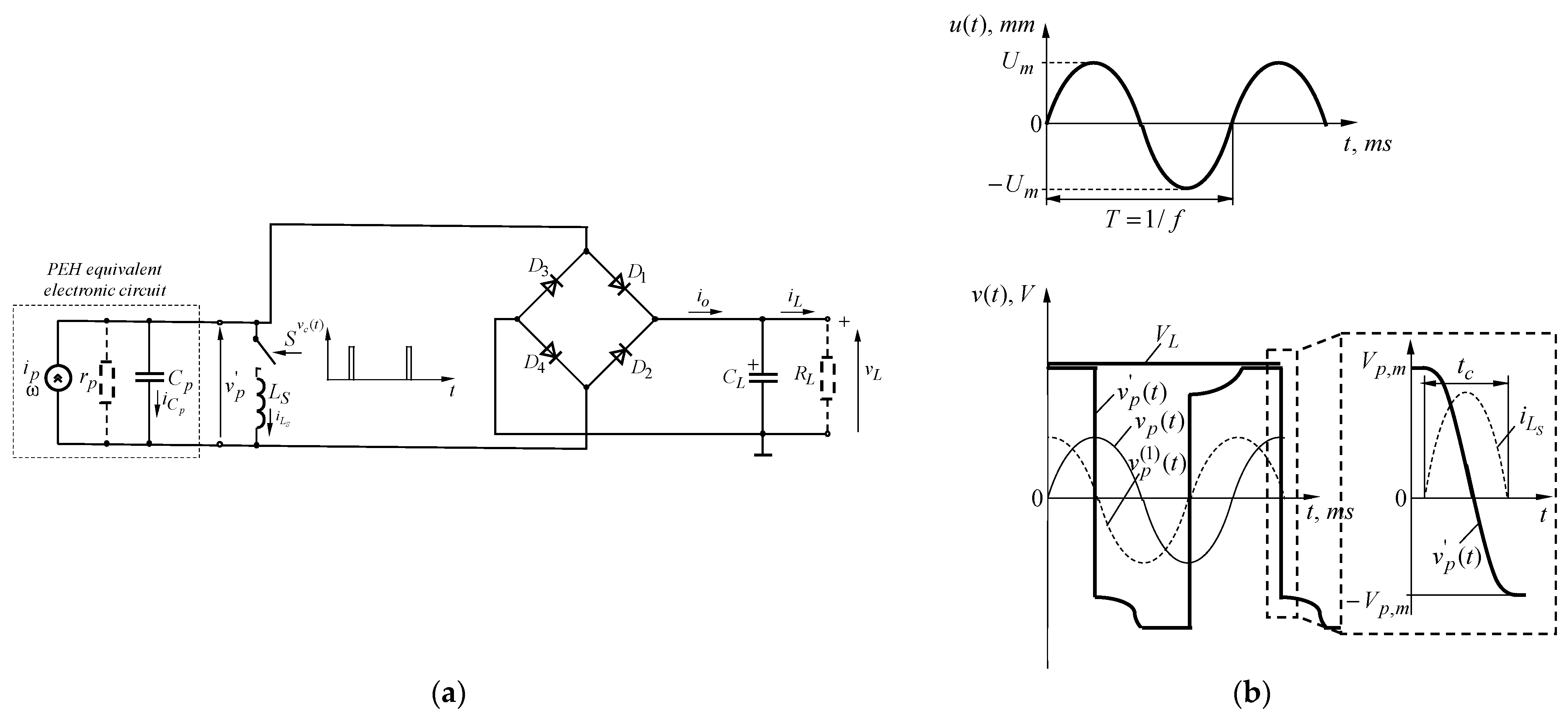
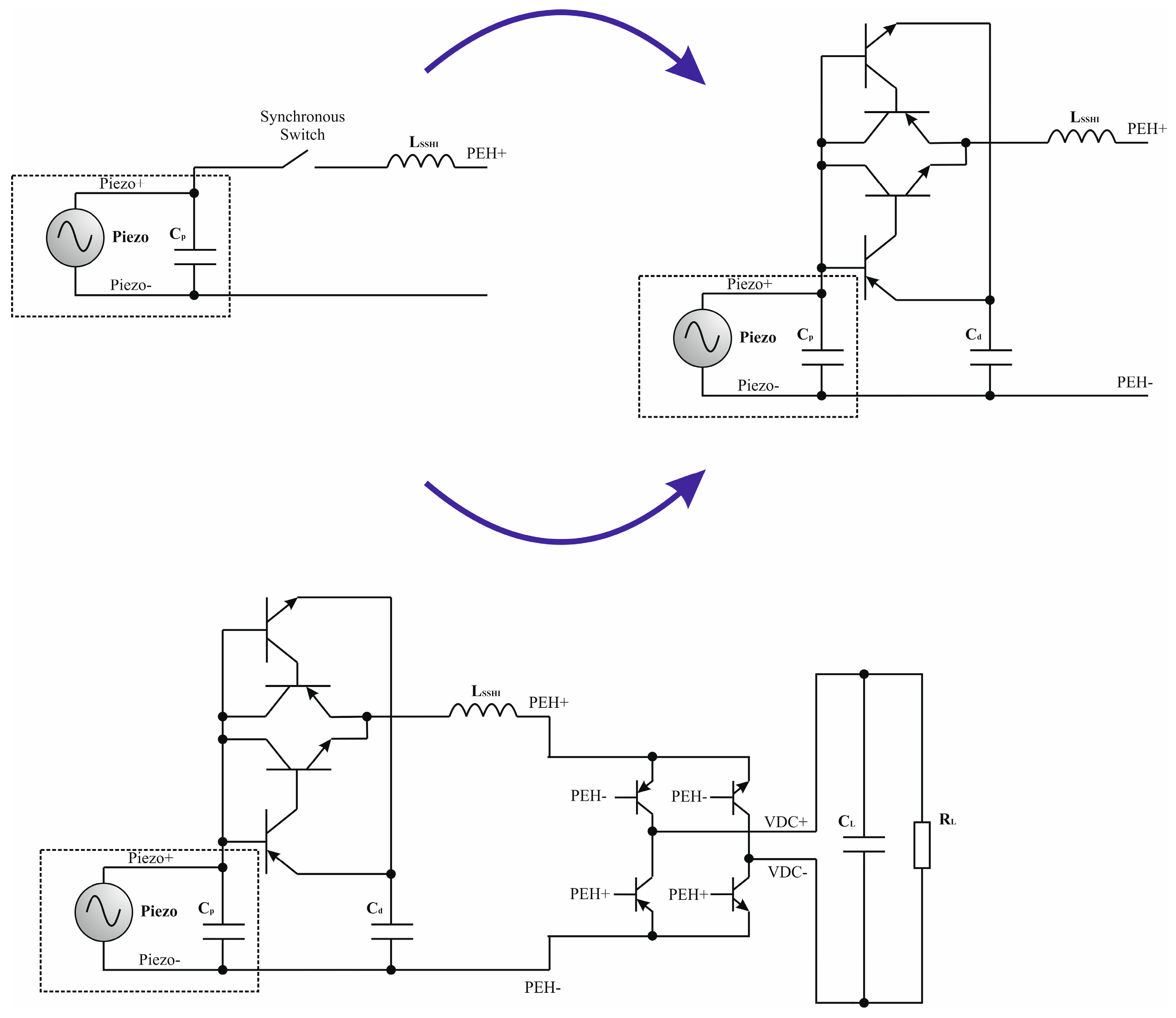
5.2. Parallel SSHI Technique—Basic Functional Circuit and Operational Principle

To reduce non-linear distortions of the v p ( t ) , as well as to increase energy efficiency, a technique is often used in which an inductor LS is connected in series to the electronic switch S, as shown in Figure 24a. This results in a parallel SSHI (Synchronized Switch Harvesting on Inductor)-based switching circuit [127]. When utilizing such a parallel SSHI (p-SSHI) technique, it is reported that an increase of 300–400% in harvested energy E H is possible compared to the standard configuration at a fixed electromechanical coupling coefficient. To illustrate the principle of operation of an input stage with a parallel SSHI, in Figure 24b [115], time diagrams of voltages in the no-load mode of operation are given. As can be seen in Figure 24a, when the switch is closed, the Cp charges LS until the inductor current iLs rises to the peak. Then, the LS charges the Cp in return until iLs falls to zero, as shown in Figure 24b. An oscillator is formed with a resonant circuit defined by Cp and LS. The electronic switch remains closed until the voltage on the piezoelectric element is reversed, as shown in Figure 24b. The time interval tc, while the switch is closed, corresponds to a half-pseudo period (or T/2) of the formed oscillator, which is equal to
t c = π L S C p .
Of the addition of the inductor LS, the waveform of the resulting signal v p ( t ) is close to a square voltage, and its first harmonic is approximately sinusoidal in form and matching the input signal v p ( t ) .
To design electronic circuits using parallel SSHI, the value of the inductance LS depends on the duration of the time interval tc, as well as on the capacitance Cp of the selected piezoelectric element. For practical applications, the value of the inductance LS is chosen to be approximately twenty to fifty times lower than the period of the mechanical vibrations [128]. The smallest value of the time interval tp is determined by the time of switching on and off the selected electronic switch.
When choosing an inductor, the losses in the resulting oscillator circuit are mainly defined by the small-signal resistance rL of the inductor and the on-state resistance RON (which for real switches is non-zero ohms) of the electronic switch. Then, the quality factor QLC of the oscillator circuit is determined as follows Q L C ρ / ( r L + R O N ) (where ρ = L S / C p is the characteristic resistance of the resonance circuit and RON is the on-resistance of the electronic switch S). The value of the resistance r L S can be determined from the known formula, at a certain inductor LS with a given value of the quality factor and R O N 0 Ω (under the condition that the on-state resistance is neglected), as
r L S 1 Q L C L S C p .
The relation between the quality factor and the piezoelectric open circuit voltage amplitude just before and just after ( V 0 , p and V 0 , p , respectively) the introducing the switching circuit with inversion is given by [131]
V 0 , p = V 0 , p e π / 2 Q L C .
When connecting a standard bridge rectifier and DC-DC converter after the electronic switch circuit, the maximum value of the average power that can be obtained through the CL (see Figure 13) is given as [131]
P o , max = α 2 ω U m 2 π C p ( 1 e π 2 Q L C )
At
V L , o p t = α C p ( 1 e π 2 Q L C ) U m ,
where α is a force factor of the piezoelectric disk, and its value is defined by the geometrical dimensions (the cross-sectional area A and inversely proportional to the thickness L of the piezoelectric generator), thus for the polarization current can be written i p = d Q d t = α u ˙ if | α C p u | V L and Q = α u is the outgoing electric charge from the piezoelectric through the bridge rectifier during the T/2 interval.
As can be seen from the above analytical expression (Formula (31)), the average power depends on the value of the quality factor determined by the inductor and the parameters of the electronic switch. For relatively large values of the quality factor, for example, when higher than 10, the average power is approximately proportional to QLC. For inductors with inductance values greater than 100 μH, it is difficult to obtain a quality factor higher than 20. In general, the quality factor of this type of passive element has typical values of up to about 50. Provided that the quality factor increases from 10 to 15, other things being equal, the power gain theoretically increases by a factor of 3.18 for the maximum average power.

5.3. Series SSHI Technique—Basic Functional Circuit and Operational Principle

The series SSHI (s-SSHI) technique is similar to the parallel SSHI, but the electronic switch and the series-connected inductor are connected in series to the piezoelectric element. Figure 25 shows the functional diagram for the series SSHI technique, as well as the waveforms of the sinusoidal excitation and the produced voltages using series SSHI. As in the circuit with parallel SSHI technique (Figure 24a), the electronic switch in Figure 25a is closed when the mechanical deflection in the vibration process reaches a maximum or minimum value. During the time intervals when the switch is closed, the electric charge passes through the inductor LS, transmitting part of the electric energy stored in the piezoelectric capacitance Cp to the output capacitor CL, connected to the output terminals of the rectifier. Figure 25b presents the corresponding time diagrams of the mechanical sinusoidal deflection and the waveform of the voltages. The value of the piezoelectric voltage at an open circuit, as well as the value of the electric charge outgoing from the piezoelectric element during the operation of the serial SSHI technique, are given by [131]
V 0 , m = V 0 , p + 2 α C p u   and
Q p = C p ( V 0 , m V 0 , p ) .
Based on Formulas (33) and (34), as well as some additional analytical transformations over the expression of the average harvested power ( P = 2 T Q p V L ), the maximum value of the average power at an optimal value of the rectified voltage related to the amplitude of the deviation has the form [131]
P max = ω 2 π 1 + e π 2 Q L C 1 e π 2 Q L C α 2 C p U m 2   at
V L , o p t = α 2 C p U m .
Then, based on Formulas (31) and (35) for the ratio of the harvested average powers in both techniques, the following expression can be obtained
( P max ) S e r i e s S S H I ( P max ) P a r a l l e l S S H I = 1 + e π 2 Q L C 2 .
As can be seen from Formula (37), for small values of the quality factor (e.g., QLC < 10) the maximum harvested average power of the serial SSHI-based circuit is approximately two times smaller than the harvested average power of the parallel SSHI-based circuit. For high values of the quality factor, the harvested powers for the two techniques are of the same value. For example, for a quality factor equal to 10 the theoretically calculated ratio of the two powers is approximately equal to 0.927. Thus, the selection of a specific technique for switching the generated piezoelectric voltage depends on the specific application of the piezoelectric energy harvesting system. When using the parallel SSHI technique, higher values of the harvested average power can be obtained. Also, higher values of the rectified voltage can be obtained for the parallel SSHI technique than for the series SSHI technique. An advantage of the series SSHI technique is that it can work with lower values of piezoelectric voltages and does not require the use of an additional power optimization circuit. Therefore, the serial SSHI technique in some cases can be realized with a smaller number of passive and active components, and as a result, smaller values of the power dissipations can be obtained.
In 2024, Osama Younas et al. innovatively proposed a method to have large passive inductors be replaced with a floating gyroinductor [132]. For the proposed electronic circuit with a floating gyroinductor as an alternative to conventional inductors, the size of the printed circuit board can be reduced. This replacement is also suitable for lower switching frequencies when larger inductor sizes are required. As a result of the replacement, a higher quality factor value can be obtained. A weakness in this method of building switchable inductors is the relatively larger number of passive and active elements, as well as the need to provide a supply voltage for the operational amplifiers used for floating gyroinductors.
The circuit diagram of a grounded gyrator is presented in Figure 26. Under the condition that the two operational amplifiers (X1 and X2) are ideal active elements ( A d 12 or v i d , 1 = v i d , 2 0 V vid,1 = vid,2 ≈ 0 V) for the voltages at their outputs, we obtain
v 1 = v i n + R 2 v i n v 2 R 3 = v i n ( 1 R 2 R 4 R 3 R 5 )   and
v 2 = v i n ( 1 + R 4 R 5 ) .
Then, for the input current and then for the input impedance is found
i i n = v i n v 1 R 1 = v i n R 2 R 4 R 1 R 3 R 5 Z i n = v i n i i n = R 1 R 3 R 5 R 2 R 4 .
When replacing the resistor R4 with a capacitor C, the input impedance is obtained with an inductive character or gyroinductor, as follows:
Z i n = j ω C 4 × R 1 R 3 R 5 R 2 = j ω C 4 R R 5 L e ,
at R 1 = R 2 = R 3 . In this way, the analytical expression for the equivalent inductance Le is simplified, and through the resistor R5, the desired value of Le can be adjusted, taking into account the tolerances of the passive components. When considering a limited value of the gain coefficients A d 1 A d 2 A d for the equivalent small-signal resistance of the gyroinductor, we obtain
r L = R 2 + R 3 R 2 A d R 1 = 2 R A d ,
at R 1 = R 2 = R 3 .
Then, based on an analysis of the formed resonant circuit, the equivalent quality factor is obtained, as follows:
Q L C = 1 r L C p / L e + L e / C p / r p ,
where r p = ( R R 5 C 4 R 5 C 4 + R C p | | r p ) A d 2 R R 5 C 4 R 5 C 4 + R C p .
The maximum value of the equivalent quality factor for real operational amplifier has the form
Q L C , max = x A d 1 A d 2 2 x 2 A d 1 + 2 A d 1 + 2 x 2 A d 2 .
at R = C 4 C p R 5 A d 1 A d 1 + A d 2 , and where x = A d 1 A d 1 + A d 2 .
As can be seen from the above formula, the value of the maximum quality factor is determined only by the gain coefficients of Ad1 and Ad2 of the two operational amplifiers.
The floating gyroinductor is obtained by connecting two gyroinductors (see Figure 26) in series on the side of resistor R5. In this case, the new value of the equivalent inductance is obtained as Le = Le1 + Le2.
In 2024, Noora Almarri et al. presented an interface circuit employing synchronized switch harvesting on a capacitor (SSHC) energy harvesting circuit. The capacitor-based synchronized switch harvesting on capacitor (SSHC) is an alternative to inductor-based methods, with this approach utilizing a set of switched capacitors [123]. The basic structure of such a circuit configuration is shown in Figure 27, courtesy of [29]. An advantage of the SSHC technique is the possibility of obtaining a smaller area of the circuit, which is particularly suitable for the implementation of an integrated circuit in compact medical devices. A weakness of switched capacitor circuits is the higher noise level, which is reflected in the stability of the output voltage.
For the circuit with single capacitor C, the output signal of the piezoelectric capacitor is generated before the piezoelectric current crosses over zero. Capacitor C will be charged through the internal capacitance Cp. In the first half cycle, the charge over the Cp is cleared only when the piezoelectric current is zero. Finally, the Cp is charged back from C in the opposite direction of the polarity. If the capacitance Cp is equal to the C, for several repetitions of flipping, the voltage Vr in steady state has the form [29]
V r = [ ( 1 4 ) n + + ( 1 4 ) 2 + 1 4 ] V R E C T .
Then,
lim n | V r | = 1 3 V R E C T .
The coefficient of the energy efficiency of such a circuit can be expressed by the following formula [29]:
η = k C k C p + ( k + 1 ) C k × 100 % ,
where k is the number of flying capacitors used in the circuit, and Ck is the capacitance of the certain flying capacitor.
As can be seen from Formula (47), the larger flying capacitors employed the higher value of the flipping energy efficiency. The energy efficiency for one-, two-, and four-stage SSHC based rectifiers will be increased with increasing ratios of the Ck/Cp.

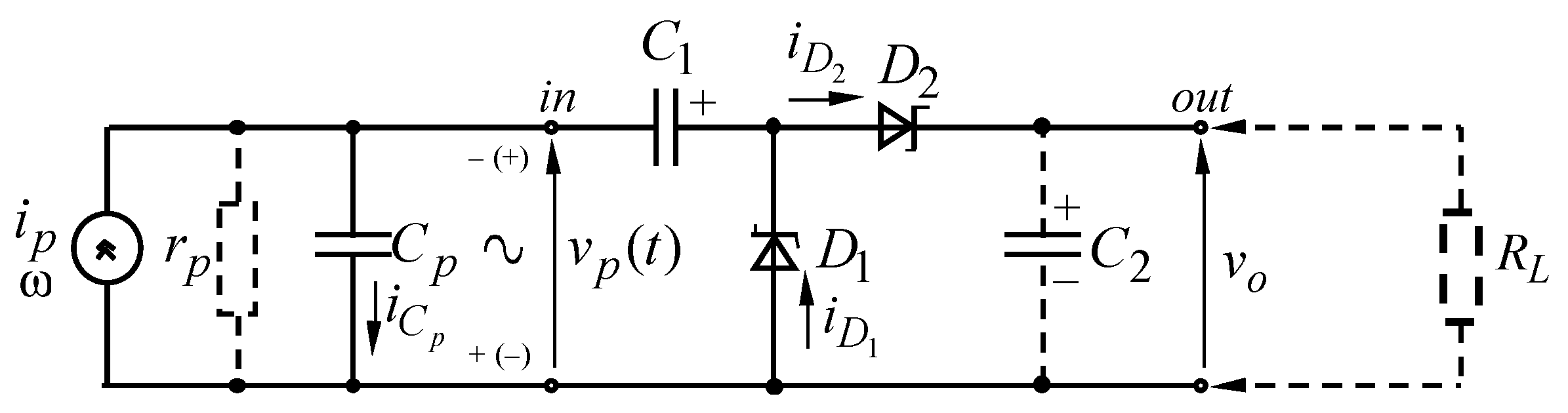
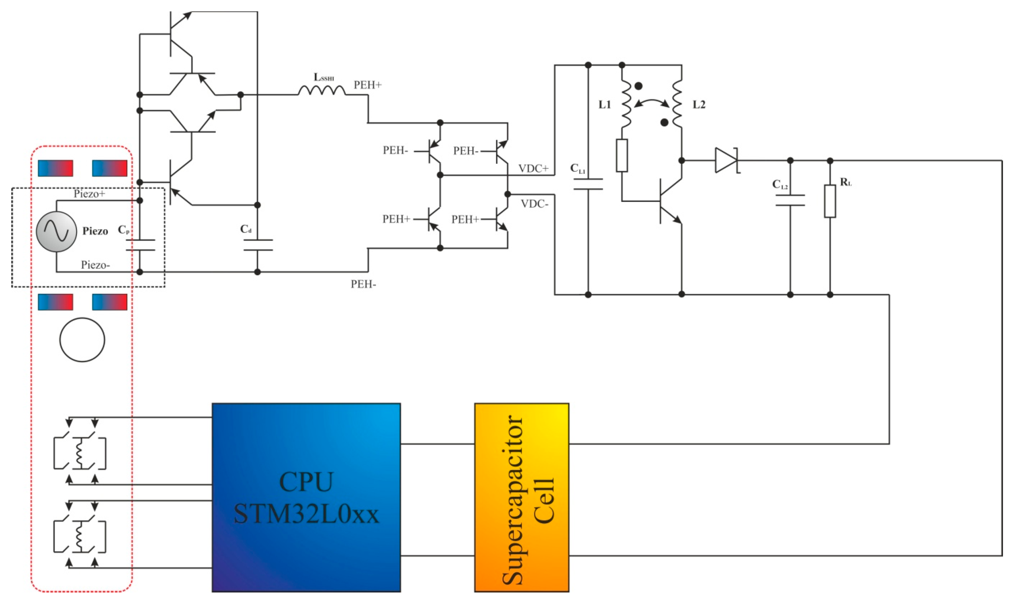
5.4. Structure and Operational Principle of a Basic Resonant Rectifier Circuits

To implement the switching of the series inductor LS in the circuits using SSHI, it is necessary to synchronize the operation of the pulse oscillator producing v c ( t ) and the input signal, which is obtained through the operation of the piezoelectric generator. For the basic structure of a resonant rectifier circuit, employing SSHI is given in Figure 28 [104,127,130]. The electronic switches in the basic structure are implemented with two MOS transistors, where M1 is an n-channel MOS transistor and M2 is a p-channel MOS transistor. A diode is connected in series to each transistor, and when M1 is turned on, diode D1 is in the forward mode of operation (the current is indicated by a red dashed line), and when transistor M2 is turned on, diode D2 is in the forward mode of operation (the current indicated by a blue dashed line).
For the implementation of the two transistors, their substrate is connected to the sources, and their drains are connected to the cathode of the D1 and the anode of the D2, respectively. Their gates are short-circuited, and the control pulse signal is obtained from the output terminal of an analog comparator U1. The non-inverting input terminal of the U1 is connected to the ground, and the inverting input is connected to the output node of the passive differentiator implemented with capacitor C1 and resistors R1 and R2. The bipolar supply voltages for the U1 are provided by the additional capacitors CS1 and CS2, as well as the rectified diodes DS1 and DS2. Moreover, the capacitors CS1 and CS2 are charged to voltages with suitable values to ensure the V D D + and V S S .
To analyze the behavior of the differentiator in the time domain, an ideal rectangular pulse is applied to the input node (Figure 29a,b). Based on an analysis of the electronic circuit, the differential equation is obtained for v p = 0 :
R 12 C 1 d v d i f d t + u d i f = 0 ,
where R 12 = R 1 R 2 R 1 + R 2 is the equivalent resistance of the voltage divider.
The solution of the above equation has the form
v d i f ( t ) = U d i f , m e t / R 12 C 1 .
To measure the settling time of the output voltage, the time constant of the circuit is defined as τ = R 12 C 1 .
The following additional condition is used to determine U d i f , m at t = 0. When the input voltage changes in a rising edge, the charge on the capacitor does not change. The output voltage repeats the direction of changing of the input voltage (Figure 29a) from zero to U d i f , m = R 1 R 1 + R 2 U p , m , then decreases exponentially according to the expression (48) again to zero. If the input voltage jumps from U d i f , m to zero (in a falling edge), then the output voltage will be jumps from zero to U d i f , m = R 1 R 1 + R 2 U p , m (Figure 29b).
If at the input node of the differentiator in Figure 30, an approximately rectangular signal with a period T for which τ < T / 2 is applied, then the output voltage is described by short pulses for each half period ( T / 2 ). This is because the capacitor is almost completely discharged for each half-cycle to zero. The smaller the time constant is compared to T / 2 , the shorter output pulses will be produced.
Of the above-described principle of operation, upon the occurrence of a pulse with amplitude U d i f , m = R 1 R 1 + R 2 U p , m , the output of the analog comparator, which is a push-pull stage, will switch to a high level for the duration of the pulse determined by the time constant of the differentiator. For the duration of the pulse, the transistor M1 turns on and flows current, providing the voltage reversal. When a pulse with an amplitude of U d i f , m = R 1 R 1 + R 2 U p , m occurs, the output terminal of the comparator will switch the output to a low level, which will turn on the transistor M2, due to which the input voltage will be reversed again. An example waveform of the control pulse vc for τ < < T / 2 is shown in Figure 30.

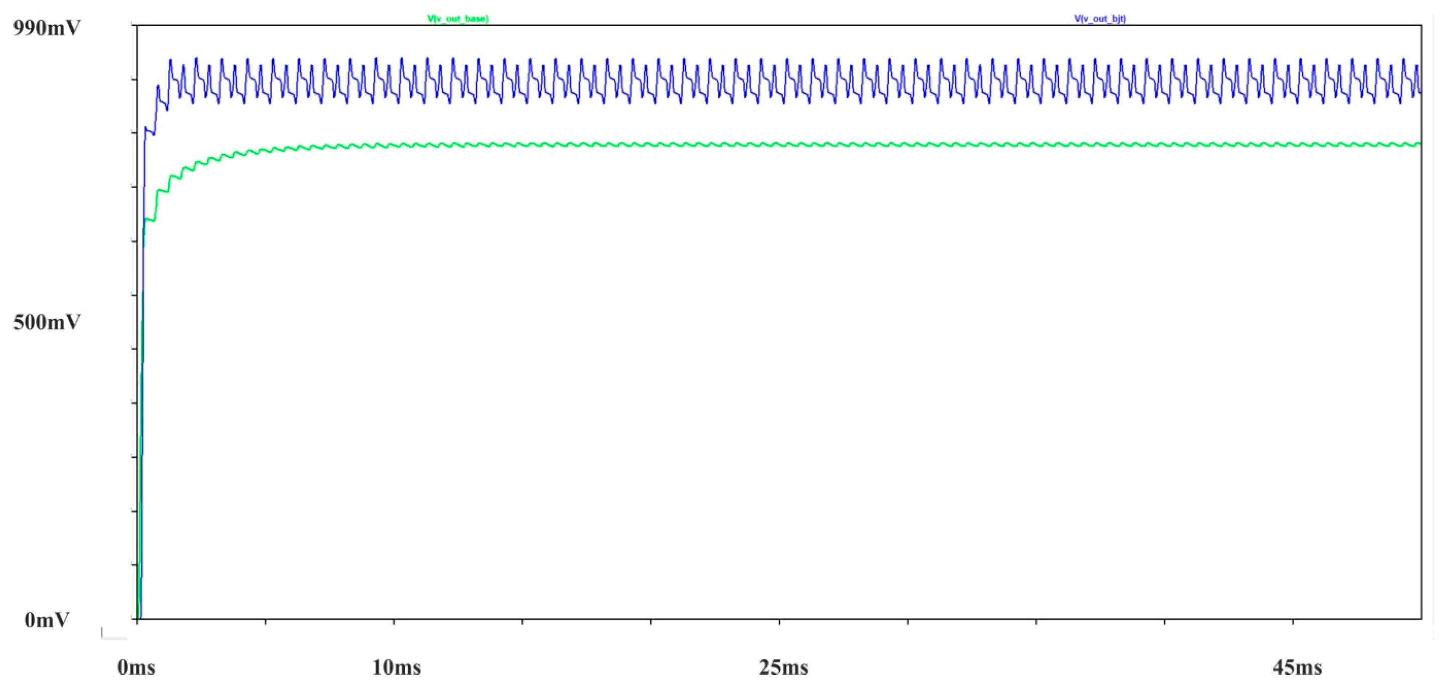
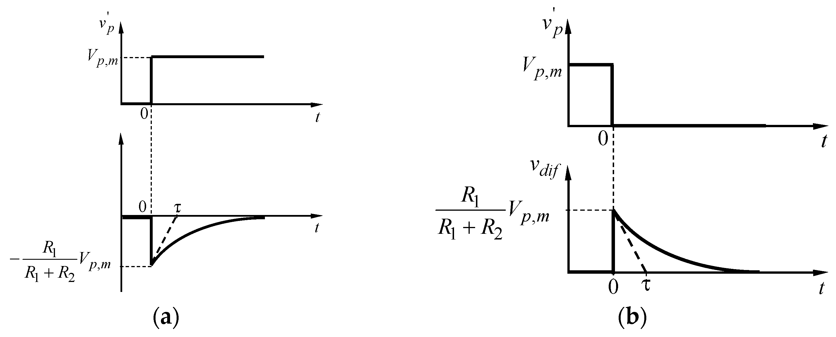
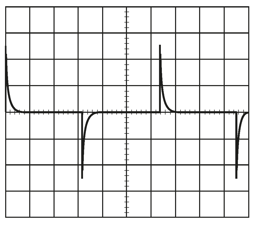
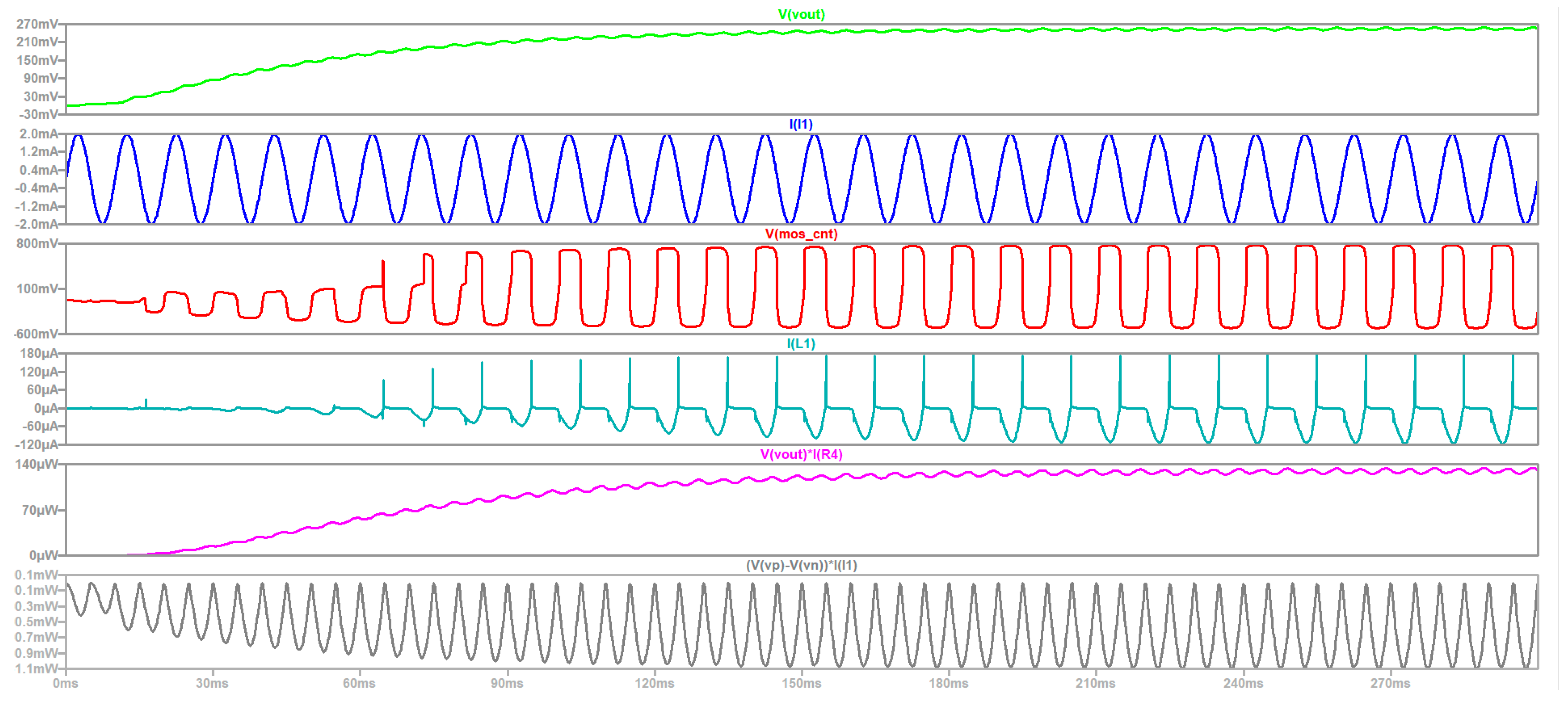
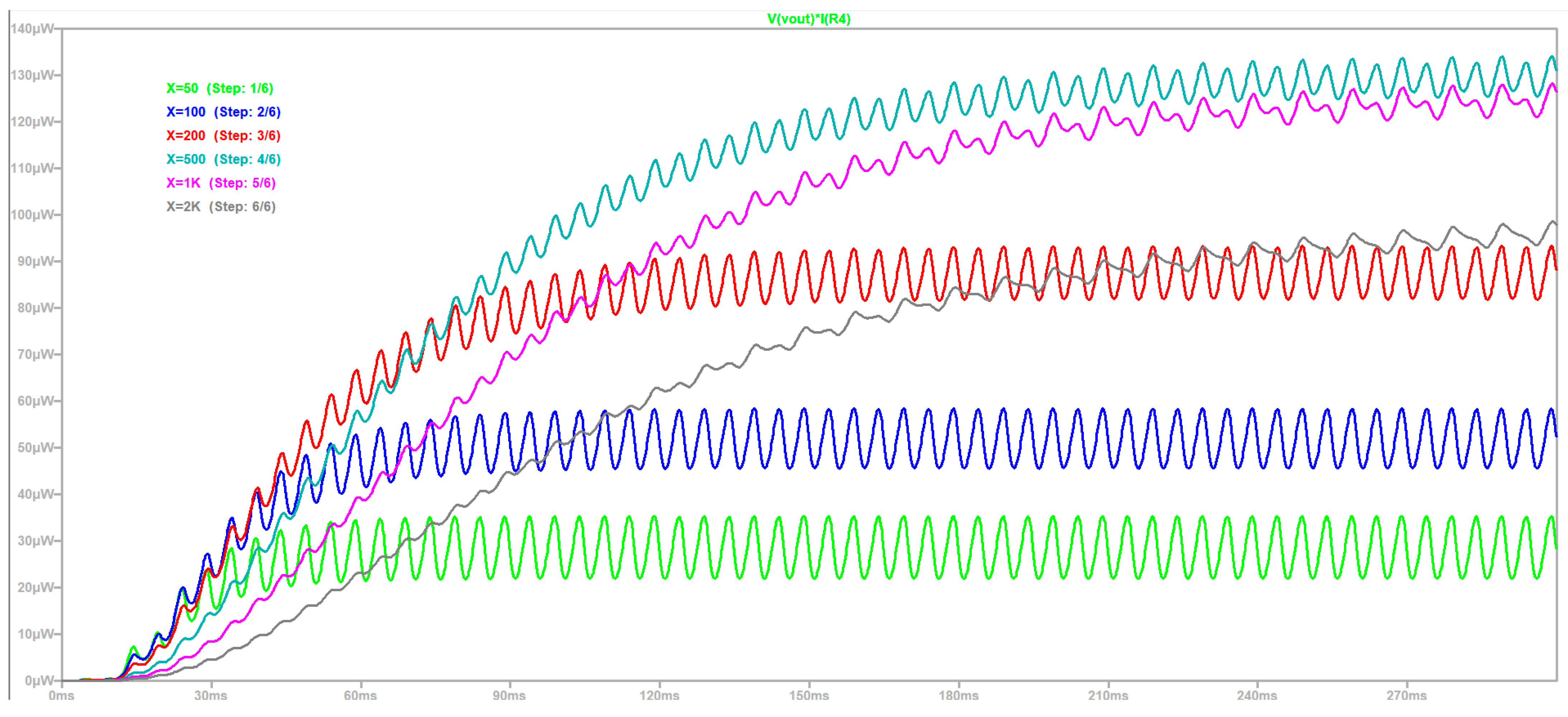
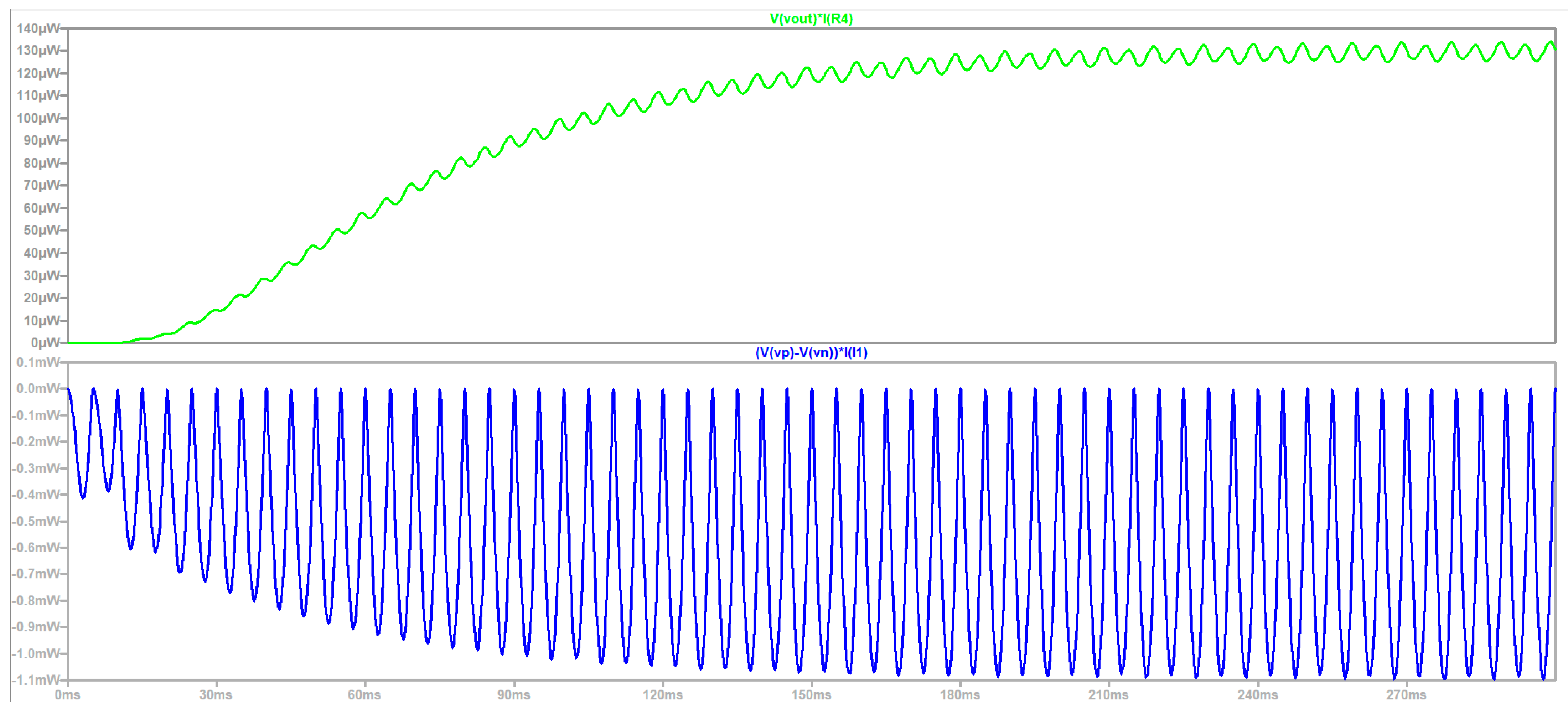
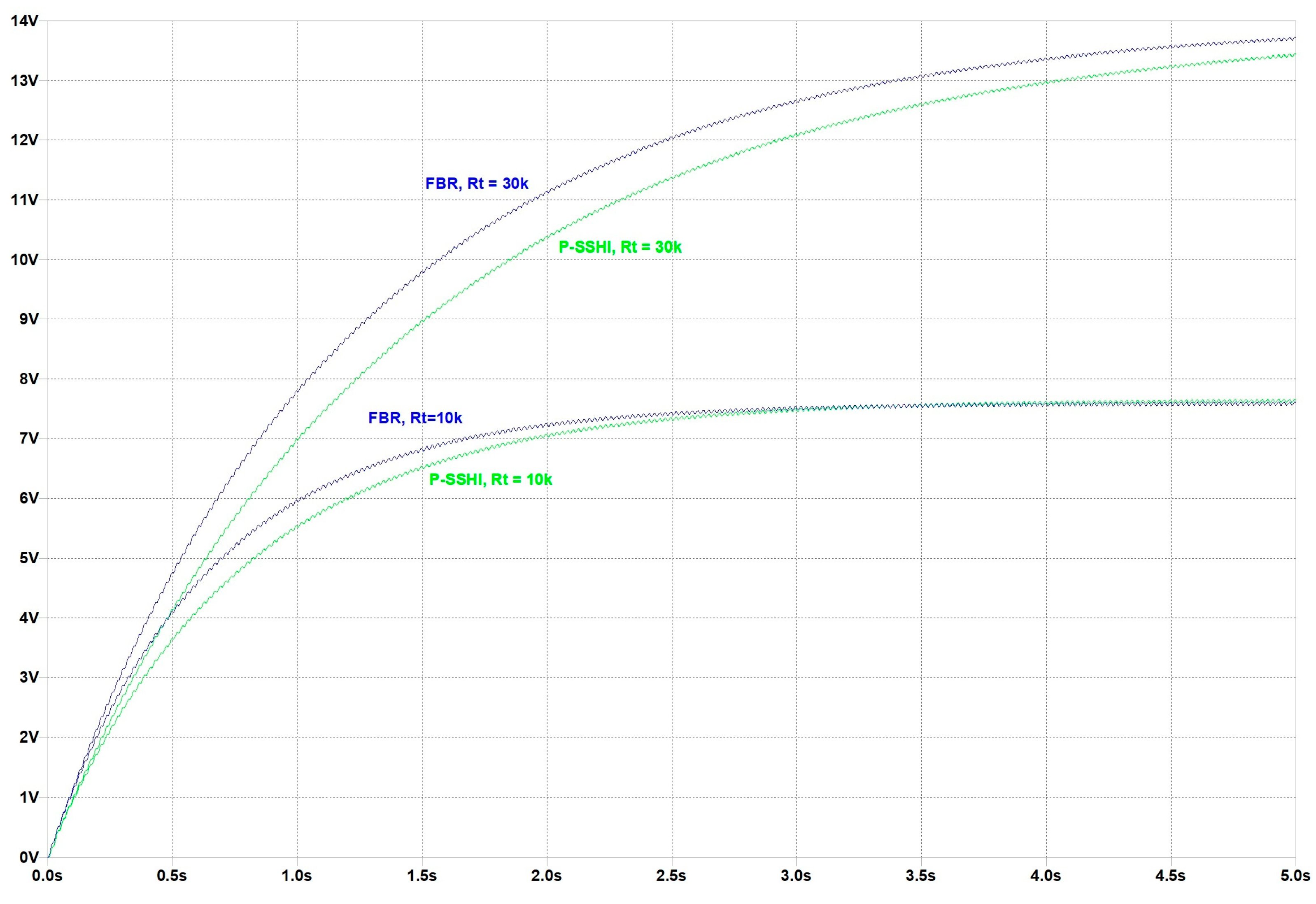
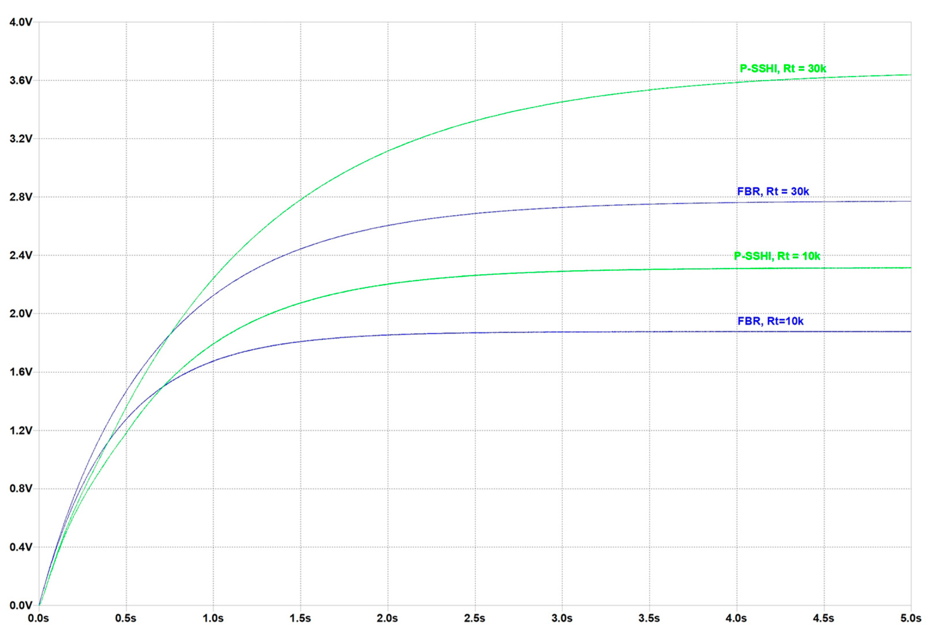
5.4.1. Simulation Testing and Discussions on Resonant Rectifier Circuit, Employing Parallel SSHI Technique

The figures below show the simulated circuit (Figure 31) of the discussed parallel synchronous switch inductor and the simulations that demonstrate its transient response (Figure 32). The input stimuli are a 1 V sinusoidal wave with a frequency of 100 Hz.
To define what the maximum output power which such a circuit can generate, we performed a parametric sweep over the load resistor’s values. The results are shown in Figure 33. The results show that the maximum output power for such a circuit is around 3 mW with high fluctuations being observed.
Additionally, in order for us to investigate what is the efficiency of such a conversion circuit, we plotted the output and input power for the system and have displayed the results in Figure 34.

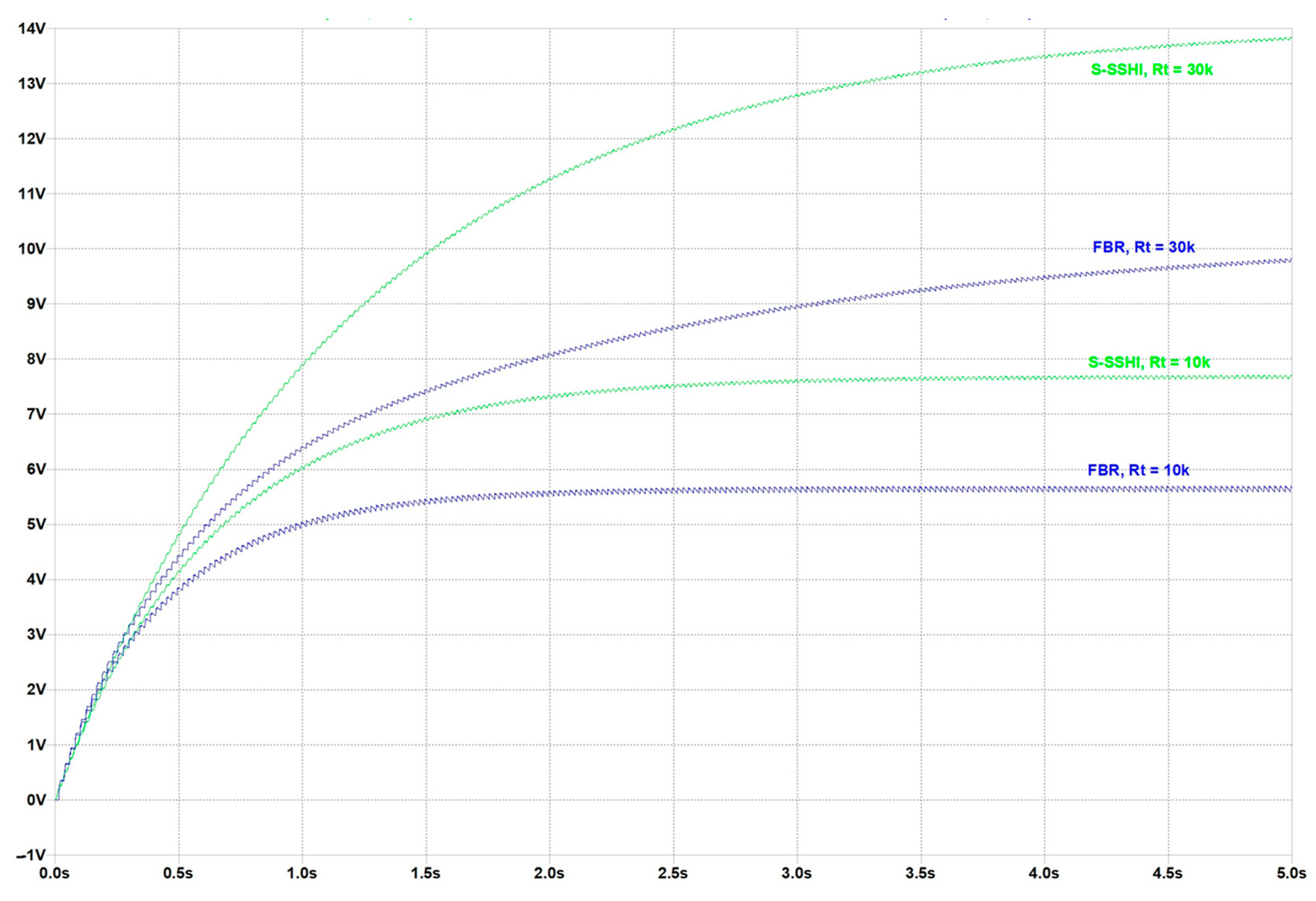
5.4.2. Simulation Testing and Discussions on Resonant Rectifier Circuit, Employing Series SSHI Technique

To achieve maximum efficiency, the storage capacitor C L value both for the standard configuration, and with the series SSHI technique must be optimally chosen. The increase in the value of the C L leads to an increase in the energy dissipated by mechanics, whilst at the same time, leads to a decrease in the energy remaining in the system [127,128]. Because of this reason, an optimal value for the C L must be chosen at the peak of the harvested energy curve. In regards to utilizing the series SSHI technique, it reduces the remaining system energy and results in a better energy transfer through the rectifier. When applying the SSHI technique to the optimal capacitance value, C L is one magnitude lower in size compared to that in the standard configuration. Figure 35 shows cases the application of such a series SSHI technique with a self-supplying BJT switch, based on the work of Fang et al. [129].
To further increase the level of the output voltage an additional boosting circuit was proposed by Kamran et al. It includes a set of coupled inductors driven by BJTs. This additional boosting circuit was added to our PEH module and shown in Figure 36 [124].
We were interested in investigating how this combination of several electronic techniques would influence the overall performance of the piezoelectric element. Because of this, we ran a series of simulation tests with the program LTSpice to analyze the presented electronic circuit (Figure 36). To perform the simulation study, simulation models of 2N3904 were used for NPN transistors, and 2N2905A was used for PNP transistors. PMEG2010AEB was used to implement the output Schottky diode. The passive components were selected with the following initial values: C d = 100 μF, L S S H I = 40 μH, C L 1 = 10 μF, L L 1 = 1 μH, L L 1 = 10 μH, R B = 10 kΩ, C L 2 = 10 μF, and R L = 1 kΩ.
Of the execution of the computer simulations, Figure 37, Figure 38, Figure 39 and Figure 40 present timing diagrams of the output voltage and output power when the circuit parameters (Figure 36) are changed. Figure 37 and Figure 38 show a simulation of how the value of the load resistor RL influences the output voltage and output power of the circuit, respectively. As can be seen (Figure 39), the increase in the load current (or decrease in the load resistance) leads to a decrease in the value of the output voltage. In this case, the authors concluded that the load should have a resistance in the range of 1–10 kΩ, in order to supply a sufficiently high voltage as the input of a following buck-boost (SEPIC—single-ended primary-inductor converter) DC-DC converter circuit. The results in Figure 31 show that the maximum output power is reached at a load resistance equal to 100 Ω. But there are noticeable fluctuations in the output power. It can be seen from the plots shown that a load resistance of 1 kΩ results in a more stable DC power output. In addition, the further increase in the load resistor’s value leading to a decrease in outputted power. This motivates the authors that the optimal load should be near 1 kΩ for the presented circuit.
To find the optimum values for some of the LC components in the circuit, we also investigated their value’s influence over the output power of the piezoelectric element. The resulting graphs are shown in Figure 39 and Figure 40.
Figure 39 shows that the increase in the value of CL1 from 10 nF to 100 nF leads to an increase in the output power of the harvester. But it can be seen that further increasing the capacitance’s value from 100 nF up to 100 μF leads to a decrease in the value of the output power. This result shows that for the given circuit, the optimal choice of the load capacitance CL1’s value is located at the maximum output power of the harvesting circuit. From our results, this optimal value was shown to be in the vicinity of 100 nF.
Similarly to the simulation performed for the optimal value of the CL1, Figure 40 shows that the optimum value of L2 has to be chosen by the PEH’s output power peak. An increase in the inductor’s inductance, value from 10 μH up to 100 μH shows a negligible difference in output power. However, increasing the value of the L2 further up to 1 mH was shown to drastically increase the PEH’s output power. Increasing the value of L2 above 1 mH was shown to decrease the PEH’s output power. The authors concluded that for the given electronic circuit, the optimal value of the L2 should be chosen close to 1 mH.

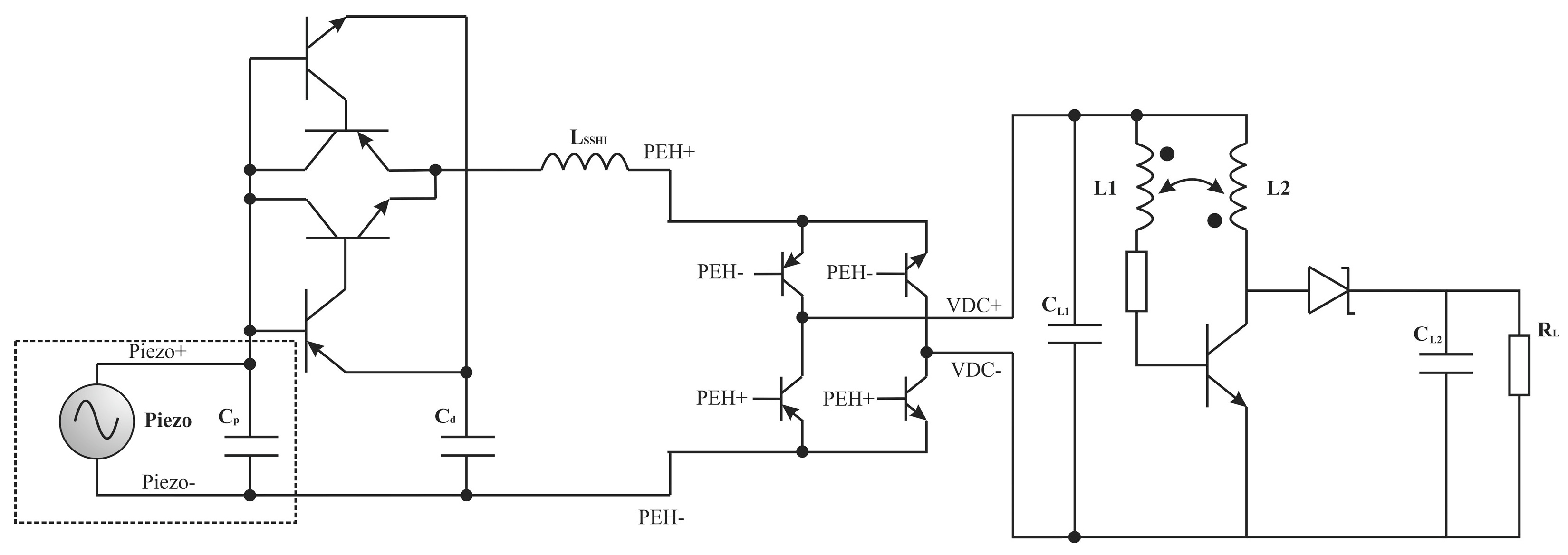
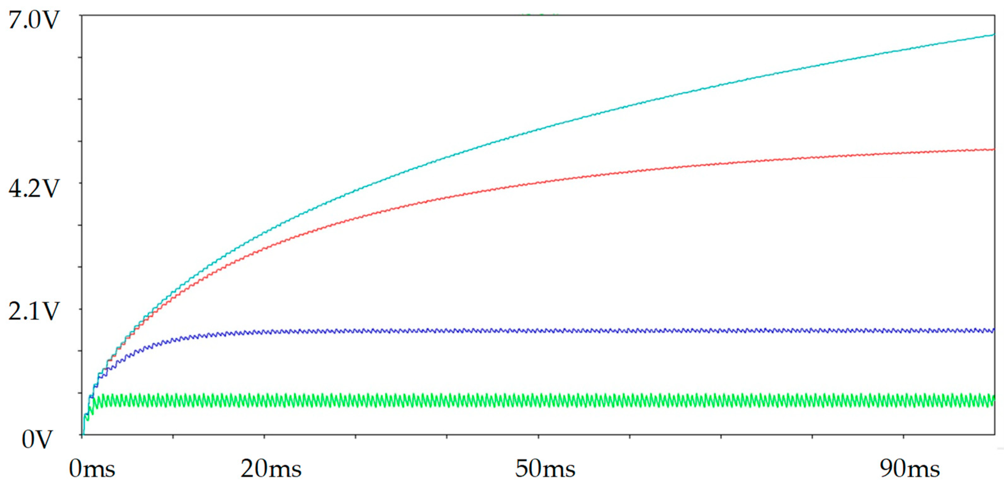
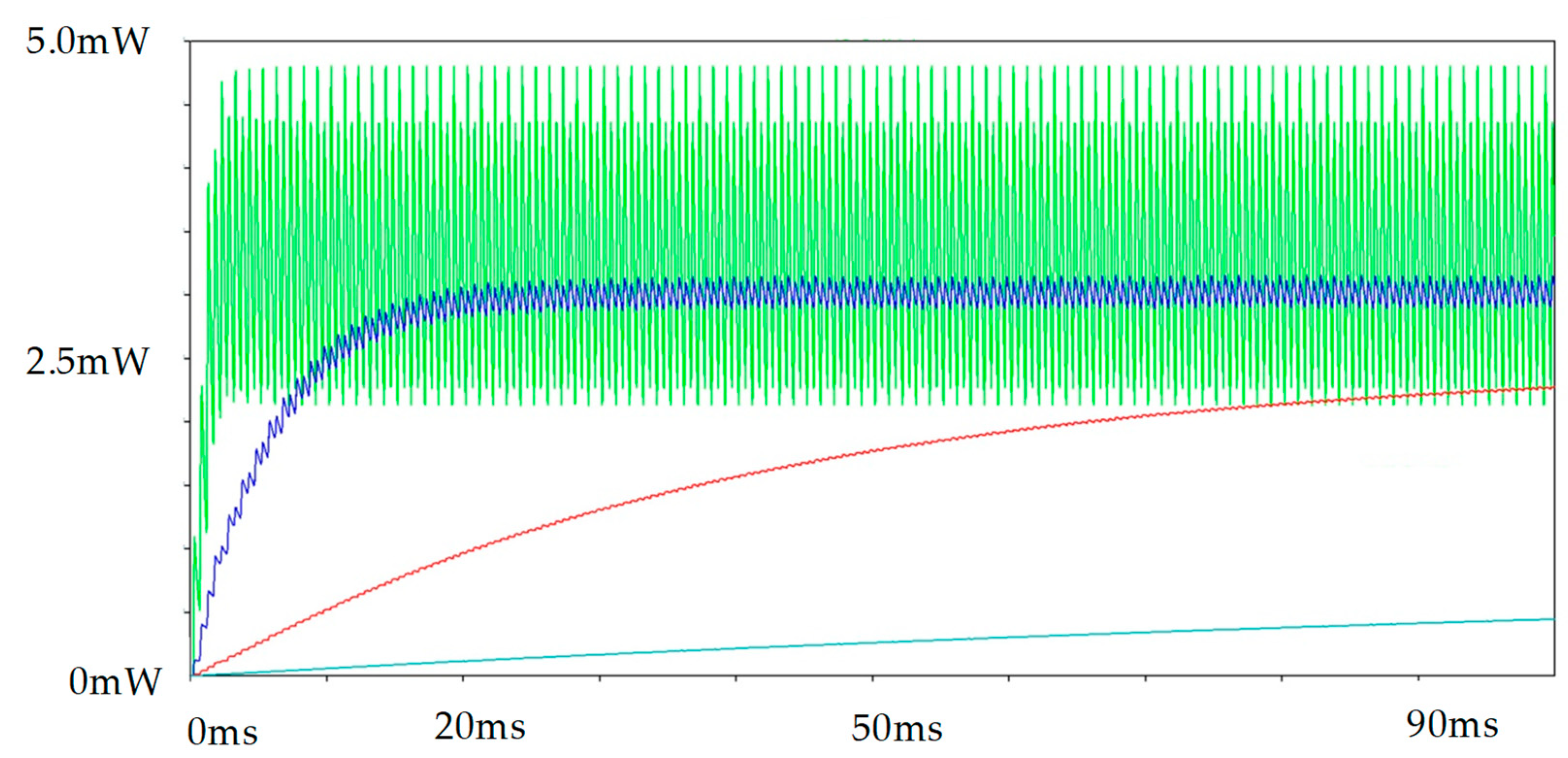
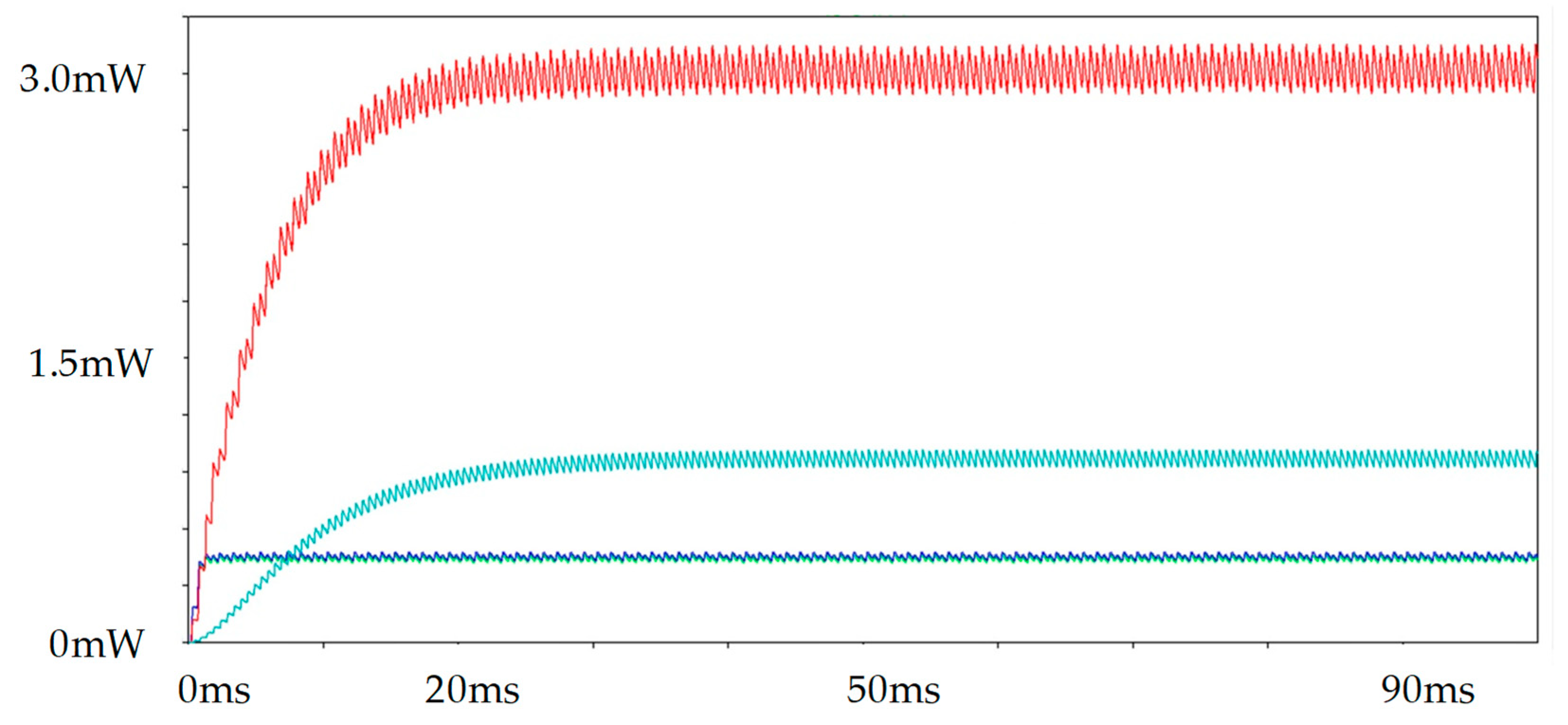
5.4.3. Simulation Results and Discussions on s-SSHI and p-SSHI Circuits, Employing a Model of Commercially Available Multilayer Piezoelectric Generator

To evaluate the performance of the synchronized switch harvesting on inductor topologies, especially parallel-SSHI (p-SSHI) and series-SSHI (s-SSHI), some computer simulations were performed by using a multilayer piezoelectric generator model. Specifically, the PPA-2011 (from MIDE Technology) piezoelectric generator was considered, with simulations conducted for two excitation frequencies as provided in the datasheet: 23 Hz and 147 Hz. The results for both resonant rectifier topologies were compared against a conventional full-bridge rectifier (FBR) (or simply bridge rectifier) under identical piezoelectric model parameters and two load resistances RL. (or marked with RT according to the simulator requirements). An estimation of power extraction performance was calculated for each circuit configuration. At a lower excitation frequency of 23 Hz, the output characteristics of the p-SSHI circuits were evaluated. The results are presented in Figure 41.
As can be seen, in this circuit, at the RT = 30 kΩ, both p-SSHI and bridge rectifier circuits yielded an output voltage of 13.6–13.7 V, resulting in no apparent improvement. At the RT = 10 kΩ, both circuits again produced identical outputs of 7.62 V.
The results for the s-SSHI circuit at the same frequency 23 Hz are presented in Figure 42. At the load resistance RT = 30 kΩ, the s-SSHI circuit provided 13.8 V, achieving a 1.983 times power increase over the bridge rectifier, where the output voltage was 9.8 V. At the RT = 10 kΩ, the output voltage was 7.8 V, marking a 1.906 times power improvement compared to the bridge rectifier circuit, where the output voltage was 5.65 V.
At a higher excitation frequency of 147 Hz, the output characteristics of the p-SSHI circuits are presented in Figure 43. As can be seen at the load resistance RT = 30 kΩ, the output voltage reached 3.65 V, which represents a 1.736 times power improvement compared to the bridge rectifier circuit, the output voltage is 2.77 V. At the RT = 10 kΩ, the output voltage was 2.32 V, which corresponds to a 1.523 times higher power than the bridge rectifier output equal to 1.88 V.
The results for the s-SSHI circuit at this frequency equal to 147 Hz are presented at Figure 44. At the load RT = 30 kΩ, the output voltage reaches 3.65 V, showing a 1.762 times power enhancement over the bridge output of 2.75 V. At the RT = 10 kΩ, the voltage reached 2.35 V, corresponding to a 1.523 times power improvement over the bridge rectifier value, equal to 1.90 V.
The simulation results demonstrate that both p-SSHI and s-SSHI circuits enhance the harvested energy relative to the conventional FBR topology for most of the studied cases. In low frequency scenarios such as 23 Hz, the p-SSHI practically does not bring any power improvements. On the other hand, for the s-SSHI topology, the improvement is more significant at lower frequencies, particularly for the s-SSHI circuit, which achieved nearly double the voltage output compared to the bridge rectifier in some cases. At higher frequencies, the performance enhancement remains substantial, with both SSHI topologies offering power gains exceeding 1.5× over the bridge rectifier.
These findings suggest that the SSHI-based rectification strategies are effective for improving the efficiency of piezoelectric energy harvesting, particularly in applications where low-frequency vibrations are predominant. The s-SSHI circuit generally outperforms p-SSHI in terms of voltage gain, making it a more suitable choice for scenarios demanding higher energy extraction efficiency.

5.5. Piezoelectric Harvester Resonant Frequency Matching and Tuning

All piezoelectric elements are designed in a manner that should produce a maximum mechanical displacement for a given external vibration source. This maximum displacement is possible only at the resonant frequency. The ambient vibrations are often not aligned in frequency with the resonant frequency of the piezoelectric elements. The piezoelectric elements have a narrowband response (or high–Q factor) close to their self-resonant frequency. The width of this response band can be expanded by decreasing the mechanical quality factor of the piezoelectric element [133].
To guarantee close to the resonant operation, because the external vibration source is unknown and independent, it is worthwhile to consider the possibility of tuning the resonant frequency of the PEH to match the ambient source’s. In order to do this in a controlled and regulated manner, electrically driven techniques for resonance tuning have been proposed in the past. This fine-tuning is typically performed by using external accelerometric sensors and an embedded MCU (microcontroller unit) [133]. By capturing the accelerometer data, the low-power CPU can evaluate the external vibration source’s frequency and fine-tune the system by controlling an electro-mechanical tuning system/actuator. Most often this system is a set of fixed constant magnets whose position relative to the piezoelectric element structure is changed thus influencing its resonant frequency, and influencing the positioning of the seismic mass [133,134]. To determine whether resonance tuning is necessary, it is important to consider what metric should be used as a toggle. The output power of the piezoelectric element might fluctuate due to frequency mismatch, but it can also decrease due to the decrease in the external vibration source’s amplitude. Because of this reason, a purely power-based measurement is not sufficient to determine whether a fine-tuning procedure should be initiated [133,135]. Another careful consideration that must be made is, as the vibration source’s mismatched frequency can be placed on either side of the resonance peak, equally displaced frequencies with a higher or lower frequency will yield the same output power-decreasing effect. For this reason, it is important to consider the frequency direction towards which the resonant frequency will be shifted [116].
There are several possible ways to influence the self-resonant frequency of the piezo harvester:
(1)
Positioning a set of constant magnets over the vibrating structure;
(2)
Adjusting the length of the cantilever;
(3)
Protruding the tip’s inertial mass.
Extending the tip of the inertial mass would require an additional micromechanical module, controlled by an external electronic circuit, wired near to the piezoelectric element. Adjusting the length of the cantilever is also troublesome due to the necessity of adding an actuator with an adjustable arm length, hence complicating the design further. The author’s opinion is that for purely practical reasons, and motivated by the necessity of simplifying the fine-tuning mechanism, the movement of a set of fixed magnets over the piezoelectric element is most optimal. To accomplish a self-adjusting system, it is best to add an external low-power CPU that will monitor the output power of the piezoelectric element and based on control software estimate whether it is necessary to adjust the magnets’ position and towards which direction. Figure 45 shows a rough block diagram of how such a system should be constructed. The low-power CPU is powered by a supercapacitor module, charged by the piezoelectric element. When a prolonged energy harvesting procedure is detected (a prolonged vibration cycle), the CPU will be woken up from its sleep mode by an external charge-duration circuit. After entering a normal operational mode, the CPU will measure the piezoelectric’s output voltage and perform a tuning check procedure. The tuning check procedure will contain an incremental step of the magnet system, controlled by a step motor. The direction of the rotation of the step motor is defined based on a randomly chosen direction and successive repeated measurements of the piezoelectric output voltage. If the output voltage decreases after the tuning step, then the direction of change must be changed. After the correct direction is found, then the CPU will perform a set of incremental steps, measuring the voltage at each step and it will stop the tuning procedure until it detects a drop in the output voltage.

5.6. Summary of Key Advances in SSHI Techniques for Piezoelectric Energy Harvesting Applications

In recent years, SSHI techniques have become a main solution for optimizing energy harvesting in piezoelectric systems. A large number of approaches have been published over the last few years. In this section, some selected works are compared, highlighting their unique features, performance, and suitability for various applications. By examining advancements in efficiency and design, this study aims to summarize the progress in SSHI technology and provide a clear perspective on its impact in addressing the challenges of miniaturization, adaptability, and performance optimization in piezoelectric energy harvesting systems. In Table 4, the most important parameters for the approaches discussed below have been summarized.
Sanchez, D. A. et al. [41] achieved impressive performance improvements over an ideal FBR, with a peak figure-of-merit (FOM) of 6.81 off-resonance and 4.4 in resonance. Its high operational efficiency (94%) includes all control circuits, and it can harness significantly more power from piezoelectric energy sources with low open-circuit voltages (670 mV). The work of Chamanian, S. et al. [44] introduces an autonomous low-profile SSHI circuit fabricated using a 180 nm CMOS process, occupying only 0.28 mm2. It offers superior power improvement (up to 5.23 times over ideal FBR) while achieving 93% voltage flipping efficiency. The compact design makes it suitable for piezoelectric harvesters with capacitances in the Nano farad range. A wearable energy harvesting system featuring a GCC-PSSHI circuit was proposed by Ammar, M.B. et al. [45], demonstrating high adaptability to low-frequency and irregular excitations such as footsteps. This solution charges capacitors and batteries efficiently and autonomously, achieving a maximum efficiency of 83.02% and providing up to 3.6 mW of output power. It also features minimal component requirements and robust cold-start capability. A fully integrated SE-SSHC rectifier that eliminates bulky external components, significantly reducing system volume was presented by Du, S. et al. [108]. By employing a split-electrode piezoelectric transducer, the design minimizes the required capacitance for voltage flipping, making it compatible with a wide range of transducer capacitances while ensuring effective energy harvesting in miniaturized systems. Çiftci, B. et al. [110] have presented an autonomous SSHCI circuit with MPPT integration. They achieved a maximum power extraction improvement of 5.44 times over the ideal FBR. Using small external inductors and a compact CMOS design (1.23 mm2), the system achieves 83% power conversion efficiency, demonstrating suitability for embedded electronics and advancing system miniaturization. Fang, S. et al. [129] introduced a series-SSHI circuit that introduces the FNOV-MPPT control method, which tracks the MPP without interrupting the energy harvesting process. Achieving a maximum MPPT efficiency of 98.1%, the design ensures a high degree of energy extraction while maintaining compactness and functionality for weakly coupled piezoelectric harvesters. The last reviewed approach conducted by Chew, Z. [130] describes a topology-switching (VD/FB) rectifier based on the piezoelectric harvester’s voltage. This ensures efficient operation across a wide range of vibrations and excitations, maintaining low power consumption (240–410 nW). The adaptive design amplifies low voltage effectively and prevents overvoltage, making it highly versatile for energy harvesting.

6. Low-Dropout (LDO) Regulators for Piezoelectric Energy Harvesting Applications: Basic Parameters of Commercially Available ICs of LDO Regulators

To obtain a stabilized value of the output DC voltage, a cascade Low-Dropout (LDO) regulator is added after the voltage rectifier. The LDO regulators are used to supply wearable electronic devices due to their ability to provide stable and efficient voltage regulation with minimal power loss. Specially designed LDO regulators with low and ultra-low quiescent currents are commonly used in devices with limited energy sources, such as piezoelectric energy harvesting systems, because of their low power losses. Typically, they are used when multiple supply voltages are required using one harvesting circuit. One of the main advantages of LDO regulators is their low-noise operation. Almost all wearable electronic devices include microcontrollers, sensors, and other components that require precise and clean power to operate effectively. Excessive noise can interfere with signal processing, especially in sensitive applications like health monitoring or fitness tracking. The LDO regulators are essential components in power management circuits, ensuring stable and low-noise power supply to sensitive electronic circuits. These linear voltage regulators maintain a constant output voltage, regardless of the fluctuations of the input voltage and the varying load conditions. Their ability to operate with a minimal voltage difference (dropout voltage) between the input and output makes them highly efficient, particularly in battery-powered and portable devices.
The LDO regulators are widely used in devices requiring low noise and precise voltage regulation, such as consumer electronics, medical instruments, and industrial systems [136]. Unlike their switching counterparts, LDOs generate less electromagnetic interference, making them suitable for applications involving sensitive analog or mixed-signal circuits. The trend toward smaller and more power-efficient devices has further elevated their importance, especially in system-on-chip (SoC) designs where integration and compactness are critical. Capacitor-less LDO designs have emerged as a solution to the removal of bulky external capacitors while improving transient response and stability [136].
The design of LDOs involves addressing several trade-offs, including efficiency, stability, and dynamic response. For instance, achieving low quiescent current is crucial for enhancing battery life in portable and IoT devices, while maintaining high transient performance ensures robustness against rapid load changes. Innovations like multi-loop stabilization and flipped voltage follower (FVF) techniques are being explored to optimize these parameters [137]. Furthermore, modern designs aim to improve metrics such as power supply rejection ratio (PSRR) and transient response without increasing size or power consumption.

6.1. Typical Circuit Diagram of an LDO. Parameter Definition

In Figure 46 a typical circuit diagram of a CMOS LDO is shown [138]. The schematic consists of a voltage reference source Vref, an error amplifier (EA), a pass pMOS transistor Mp, and voltage feedback, consisting of the resistors RF and RN. The RC group of the CoA and roA model the output impedance of the error amplifier, as well as the CL and RL simulate the input impedance of the external load. More details about the calculations of the pole frequencies are presented in [138].
For an ideal operational amplifier, the transfer function has the form
V L = ( 1 + R F R N ) A V × V r e f .
Regarding the input and the output parameters of the circuit—VRECT (the rectified voltage or the storage voltage over the energy storage element), VL, and IL we could define the Line Regulation (LR) as well as the Load Regulation (LDR):
L R = Δ V L Δ V R E C T = Δ A d A d 1 1 + β A d Δ β β = Δ A d A d 1 F Δ β β   and
L D R = Δ V L Δ I L 1 β A d g m p ,
where Δ β β = R F R N + R F ( Δ R N R N Δ R F R F ) is the relative change in the negative feedback coefficient, F = 1 + β A d is the depth of the negative feedback, and A d is the open-loop voltage gain. Also, less instability can occur at greater depth F = 1 + β A d β A d at β A d > > 1 .
As can be seen in Formula (51) the line regulation coefficient is determined by the relative change in the parameters of the negative feedback coefficient through the manufacturing tolerances ( Δ R N / R N and Δ R F / R F ) and temperature coefficients of the resistors T K R = Δ R R . 1 Δ T , % / ° C .
As those equations show, the load regulation represents the ability of the LDO to maintain a constant output voltage while the output current changes. On the other hand, the line regulation represents the ability to keep the output voltage while the input voltage is changing. Quantitively, this could be estimated by the so-called Power Supply Rejection Ratio (PSRR). This parameter represents the ability of the regulator to suppress variations in VRECT, affecting VL and it could be defined by
P S R R = 20 log 10 Δ V L Δ V R E C T .
Then, the energy efficiency of the LDO is defined by:
η = P o P i n × 100 % = V L × I L V R E C T ( I L I Q ) × 100 % ,
where IQ is the quiescent current of the error amplifier.
For the implementation of an error amplifier, differential amplifiers using MOS transistors or basic MOS differential-pair configuration are most often used. To obtain a higher voltage gain, differential amplifier configurations with current-source loads are used. To further increase the gain, so-called cascode differential amplifiers are also used. In this way, telescopic cascodes are obtained because the stacking of several MOS transistors resembles the extension of a telescope [119]. In the implementation of low-voltage LDO regulators, the use of telescopic cascodes can be replaced by the construction of a folded-cascode amplifier. In this way, a high value of the amplification factor can be obtained without increasing the value of the supply voltage and without increasing the current consumption in the circuit. Based on an analysis of the basic folded-cascode amplifier circuit built using CS (common-source) and CG (common-gate) transistors, for the frequency of the dominant pole we can write
f p = 1 2 π r o A ( C o A | | C G S p ) 1 2 π r o A C G S p .
Then, for the unity-gain frequency, we find
B 1 = G m r o A f p G m 2 π r C G S p
From a design point of view, the capacitance CGSp is suitable to be of such value that for the frequency B1 the phase shift does not exceed 135°, which ensures stable operation of the electronic circuit. If the capacitance CGSp is not sufficiently large in a given case, then an additional capacitor CM can be connected in parallel to the CGSp. It is important to note that as the capacitor CM increases, the phase margin also increases. In other words, a larger capacitance CM reduces the error amplifier bandwidth but does not impair its response (which can happen when the phase margin decreases). Of course, in the design process, the capacitor CM can be increased to obtain the phase margin to its required value.

6.2. Recent Advances of LDOs. Comparative Analysis

A comparative analysis represented in Table 5 was made to overview key parameters for selected LDO designs drawn from recent approaches. The selection of works is mainly based on devices with low power losses which are suitable for wearable power supplies. These works were chosen for their focus on innovative solutions to enhance LDO performance, making them highly relevant for modern low-power, and wearable electronic applications. The selection includes designs optimized for capacitor-less operation, ultra-low power consumption, improved transient response, and robust noise immunity. These features are critical for devices like wearables, Internet of Things (IoT) systems, and portable electronics, where efficiency, compactness, and reliability are paramount.
The comparison examines essential parameters such as the technology node, output voltage, dropout voltage, quiescent current, load regulation, PSRR, settling time, and unique features. The technology node reflects the level of integration and power efficiency achievable, with advanced nodes such as 55 nm CMOS offering improved scalability. Parameters like dropout voltage and quiescent current highlight the designs’ energy-saving capabilities, essential for prolonging battery life in wearable devices. Load regulation and PSRR provide insight into the stability and noise resilience of each design, ensuring consistent performance under varying load conditions and in noisy environments. Settling time demonstrates the responsiveness of the LDO, a key parameter for systems that demand fast adaptation to dynamic loads. Additionally, unique features such as capacitor-less architecture, event-driven control, and ESD protection distinguish these works by addressing specific challenges in their target applications.
In ref. [136] Koniavitis, K. et al. describe a multiloop stabilized LDO regulator, emphasizing its low voltage operation and small compensation capacitor, which reduces the used chip area. The regulator demonstrated stability across process, voltage, and temperature (PVT) variations, with a high phase margin, showcasing its robustness for future use in integrated systems. Sun, M. et al. [137] present a capacitor-less LDO design suitable for digital-analog hybrid circuits, achieving stability even without on-chip capacitors by employing an RIPO and SSFB technique. The design’s ability to handle a wide load current range with an efficient transient response was highlighted. The approach from Pé-rez-Bailón, J. et al. [138] focuses on an output capacitor-less LDO regulator optimized for battery-powered devices. With its low quiescent current and relatively small chip area, this design is characterized by its good transient performance and efficiency, providing a viable solution for portable on-chip applications. Khan, D. et al. [139] explore the integration of multiple LDOs in a power unit for SoC applications, demonstrating high PSRR and load regulation. It highlights the stability of the LDOs across various output voltages (1.5 V, 3 V, 5 V) and their performance in delivering stable outputs under varying load conditions. Gao, M. et al. [140] discuss a high-speed LDO that incorporates transient enhancement techniques. The use of a class AB super source follower and an active capacitor circuit results in fast transient responses and low overshoot/undershoot, making the LDO suitable for automotive sensor chips. Serra-no-Reyes, A. et al. [141] present a compact LDO regulator using reverse nested Miller compensation, designed for enhanced regulation, dynamic response, and power efficiency. The LDO shows stable operation across a wide input voltage range and load current variations, reducing transient overshoot and undershoot, thus offering a compact, power-efficient solution for low-power devices. Seo, U.-Y. et al. [142] introduce an LDO regulator with integrated ESD protection, They claim that the LDO shows stable voltage output under load current variations. The proposed design proves its suitability for mobile applications requiring robust voltage regulation and high reliability in the face of potential IC damage from ESD events. Christos K. et al. [143] discuss a D-LDO designed for ultra-low-power and ultra-low-voltage IoT applications. The use of a burst oscillator allows for instant load response, offering exceptional power efficiency and a significant improvement in power efficiency compared to analog LDOs. This design is ideal for IoT systems requiring low quiescent current and high efficiency.

6.3. Commercially Available IC of LDOs

Building on the previous section, which analyzed innovative scientific approaches to LDO design, in this section commercially available LDO are compared. Only devices with low and ultra-low quiescent current are selected which are suitable for wearing applications. In Table 6 selected ICs with low quiescent current, which are mainly suitable for wearing devices are presented.
Table 6 provides a comparative analysis of six commercially available low-dropout regulators [144,145,146,147,148,149], showing their capabilities and suitability for different applications. The first two ICs that are compared are TPS7A16A-Q1 [144] from Texas Instruments (Dallas, TX, USA) and MAX15007 [147] from Analog Devices (Wilmington, MA, USA). They are designed for automotive and industrial systems, offering high reliability and broad input voltage ranges. The ICs specially designed for portable electronics are XC6206J [145] from Torex (Tokyo, Japan), STLQ015 [146] from STMicroelectronics (Geneva, Switzerland), and MIC5365 [148] from Microchip Technology (Chandler, Arizona, USA). They are characterized by ultra-low quiescent currents, which optimize battery life. Lastly, the LP5907 [149], also from Texas Instruments, delivers excellent high PSRR, making it an ideal choice for noise-sensitive analog circuits. This comparison highlights how manufacturers tailor LDO designs to balance energy efficiency, robustness, and noise performance across diverse applications.

7. Conclusions

In recent years, wearable electronic devices have grown in popularity, especially for health monitoring. These devices require power supplies that are small, lightweight and well-integrated into the human body. Traditional batteries pose challenges due to their limited lifespan, large size, and the need for frequent replacements. To address these problems, battery-free power supplies combining supercapacitors with piezoelectric generators are discussed. They offer good efficiency and smaller form factors. Furthermore, low-power integrated circuits, such as synchronized switch harvesting on inductors (SSHIs) and LDO regulators are presented. These circuits help to simplify power management and reduce the overall size of wearable devices.
In this paper, the focus of the authors’ attention was placed on the analysis of circuit configurations suitable for the development of wearable battery-free power supply devices. The functioning of this class of battery-free power supplies involves the use of thin-film piezoelectric input generators, which convert the energy of mechanical vibrations spontaneously arising as a result of human activity into electrical energy. Since the analysis was concentrated on the application of power sources in biomedical signal processing systems, the paper presented an overview of contemporary thin-film piezoelectric generators. The paper analyzed the structure, the principle of operation, and the most important parameters that can be used as a basis for forming the parameters of the internal equivalent impedance of the generators. Due to the specific structure, method of use, and values of the electrical parameters of thin-film piezoelectric generators, the selection of an appropriate circuit configuration of the input stage, converting AC to DC voltage, is essential for obtaining a sufficient value for the energy efficiency coefficient. The structure, operating principles, and the most important parameters of various circuit configurations suitable for the design of input stages for thin-film piezoelectric piezo harvesters were analyzed in the greatest detail. In reviewing the input stages, the authors have tried to point out the advantages and disadvantages of each circuit, depending on the specific source, the designer can choose the most suitable configuration. The authors have presented a design approach that indicates the various available compromises when selecting a circuit configuration and when selecting component values for a given configuration. This approach is characteristic of the design most often of analog circuits, which are largely the input stages in the circuits for converting AC to DC voltage. Unlike digital circuits, there are still no algorithms and programs for analog and analog circuits with pulse output that would fully ensure the design process. This is due, on the one hand, to the wide variety of options for a given type of circuit, and on the other hand, in some cases, it is relatively difficult to cover the issue in a purely theoretical way, since there are often mutually contradictory requirements. To a significant extent, the design of analog circuits requires specialized knowledge and skills acquired through many years of experience. The analog circuits are more sensitive to non-idealities and any other second and higher-order effects, as well as to parasitic interference (“interference” between channels, noise from transistor substrates, noise from external sources, etc.). In the group of analog circuits, the subjects of consideration were bridge rectifiers using Schottky diodes or transistors (BJTs and MOSFETs) and voltage-doubler rectifiers implemented with Schottky diodes and an active diode with regulation loop, composed by an op-amp. The paper does not consider multipliers with a higher multiplication factor, since for thin-film piezo harvesters there would be a limitation in the level of the rectified output voltage. In the group of analog circuits with pulsed output, the subject of analysis is SSHI (Synchronized Switch Harvesting on Inductor) based energy harvesting circuits, connected before the voltage rectifier to increase the amplitude of the AC voltage. To illustrate the practical applicability, an electronic circuit implementing the SSHI technique with an output-coupled inductor booster was studied. Based on computer simulations for sample electronic circuits, the influence of various parameters on the level of the output rectified voltage and the output power was studied. Of the performed analysis, a practical approach for piezoelectric harvester resonant frequency matching and tuning was proposed.
To provide a stable and low-noise power supply to sensitive electronic circuits, the structure and principle of operation of a typical schematic diagram of a CMOS low-dropout (LDO) regulator were analyzed in the paper. Also, the key parameters for selected LDO designs drawn from recent approaches were presented. Based on a comparative analysis, the most important advantages and disadvantages were discussed and the possibilities for use in wearable electronic devices were considered. In addition to the presented custom LDO designs, reported during the last five years, the electrical parameters of the commercially available IC of LDOs, suitable for the design of electronic systems of low-power piezoelectric energy harvesting circuits for wearable power supply devices, were also systematized.
Looking ahead, the opportunity to develop self-sustaining wearable devices powered by body heat, movement, or biochemical reactions is promising. More efficient power management and energy harvesting systems could lead to smaller, longer-lasting wearable electronics. However, challenges in miniaturization, cost, and stability must be addressed for these solutions to become widely adopted in commercial products. Based on the analysis presented in this paper within the framework of project BG-RRP-2.004-0005, the future work of the authors is to synthesize electronic circuits of micro-power piezoelectric energy harvesting circuits for wearable battery-free power supply devices. The electronic circuits are intended to be implemented on flexible printed circuit boards and to provide the ability to obtain several stabilized DC voltages in the range from 1.2 V to 3.3 V and output power of no less than a few mW.

Author Contributions

Conceptualization, I.P., M.A., N.K. and S.R.; methodology, I.P.; formal analysis, I.P., M.A., N.K. and S.R.; investigation, I.P., M.A., N.K. and S.R.; resources, I.P., M.A., N.K. and S.R.; writing—original draft preparation, I.P., M.A., N.K. and S.R.; writing—review and editing, I.P., M.A., N.K. and S.R.; supervision, I.P. All authors have read and agreed to the published version of the manuscript.

Funding

This work has been accomplished with financial support from the European Regional Development Fund within the Operational Programme “Bulgarian National Recovery and Resilience Plan”, procedure for direct provision of grants “Establishing of a network of research higher education institutions in Bulgaria”, and under project BG-RRP-2.004-0005 “Improving the research capacity and quality to achieve international recognition and resilience of TU-Sofia (IDEAS)”.

Data Availability Statement

Dataset available on request from the authors.

Conflicts of Interest

The authors declare no conflicts of interest.

References

  1. Kang, M.; Yeo, W.-H. Advances in Energy Harvesting Technologies for Wearable Devices. Micromachines 2024, 15, 884. [Google Scholar] [CrossRef] [PubMed]
  2. Kong, T.; Hedayatipour, A. Oximeter for All: An Innovative Look in Inclusive Physiological Monitoring. IEEE Circuits Syst. Mag. 2024, 24, 43–44. [Google Scholar] [CrossRef]
  3. Durbha, R.; Koomson, V. ChromaSense-Empowering Health, Empowering You. IEEE Circuits Syst. Mag. 2024, 24, 45–46. [Google Scholar] [CrossRef]
  4. Nangobi, Z.; Rodgers, M.; Nadunga, C. Your Health Application. IEEE Circuits Syst. Mag. 2024, 24, 47–48. [Google Scholar] [CrossRef]
  5. Fu, H.; Jiang, J.; Hu, S.; Rao, J.; Theodossiades, S. A multi-stable ultra-low frequency energy harvester using a nonlinear pendulum and piezoelectric transduction for self-powered sensing. Mech. Syst. Signal Process. 2023, 189, 110034. [Google Scholar] [CrossRef]
  6. Shuvo, M.M.H.; Titirsha, T.; Amin, N.; Islam, S.K. Energy Harvesting in Implantable and Wearable Medical Devices for Enduring Precision Healthcare. Energies 2022, 15, 7495. [Google Scholar] [CrossRef]
  7. Friebe, M. Innovation design for the future of health. In Novel Innovation Design for the Future of Health: Entrepreneurial Concepts for Patient Empowerment and Health Democratization; Springer: Cham, Switzerland, 2022; Chapter 1; pp. 1–13. ISBN 978-3-031-08190-3. [Google Scholar]
  8. Song, Y.; Min, J.; Yu, Y.; Wang, H.; Yang, Y.; Zhang, H.; Gao, W. Wireless Battery-Free Wearable Sweat Sensor Powered by Human Motion. Sci. Adv. 2020, 6, eaay9842. [Google Scholar] [CrossRef]
  9. Li, C.; Jiang, F.; Liu, C.; Liu, P.; Xu, J. Present and Future Thermoelectric Materials Toward Wearable Energy Harvesting. Appl. Mater. Today 2019, 15, 543–557. [Google Scholar] [CrossRef]
  10. Todaro, M.T.; Guido, F.; Algieri, L.; Mastronardi, V.M.; Desmaële, D.; Epifani, G.; De Vittorio, M. Biocompatible, Flexible, and Compliant Energy Harvesters Based on Piezoelectric Thin Films. IEEE Trans. Nanotechnol. 2018, 17, 220–230. [Google Scholar] [CrossRef]
  11. Khalifa, S.; Lan, G.; Hassan, M.; Seneviratne, A.; Das, S.K. HARKE: Human Activity Recognition from Kinetic Energy Harvesting Data in Wearable Devices. IEEE Trans. Mob. Comput. 2018, 17, 1353–1368. [Google Scholar] [CrossRef]
  12. Seneviratne, S.; Hu, Y.; Nguyen, T.; Lan, G.; Khalifa, S.; Thilakarathna, K. A Survey of Wearable Devices and Challenges. IEEE Commun. Surv. Tutor. 2017, 19, 2573–2620. [Google Scholar] [CrossRef]
  13. Mukhopadhyay, S.C. Wearable Sensors for Human Activity Monitoring: A Review. IEEE Sens. J. 2014, 15, 1321–1330. [Google Scholar] [CrossRef]
  14. Wang, Z.-q.; Huang, Z.-h. Wearable health status monitoring device for electricity workers using ZigBee-based wireless sensor network. In Proceedings of the 2014 7th International Conference on Biomedical Engineering and Informatics, Dalian, China, 14–16 October 2014; pp. 602–606. [Google Scholar] [CrossRef]
  15. Maciuca, A.; Popescu, D.; Strutu, M.; Stamatescu, G. Wireless sensor network based on multilevel femtocells for home monitoring. In Proceedings of the 2013 IEEE 7th International Conference on Intelligent Data Acquisition and Advanced Computing Systems (IDAACS), Berlin, Germany, 12–14 September 2013; pp. 499–503. [Google Scholar] [CrossRef]
  16. Wearable Technology Market. September 2024. Available online: https://www.precedenceresearch.com/wearable-technology-market (accessed on 8 March 2025).
  17. Hannan, M.A.; Mutashar, S.; Samad, S.A.; Hussain, A. Energy harvesting for the implantable biomedical devices: Issues and challenges. Biomed. Eng. Online 2014, 13, 79. [Google Scholar] [CrossRef] [PubMed]
  18. Bandodkar, A.J.; Wang, J. Wearable Biofuel Cells: A Review. Electroanalysis 2016, 28, 1188–1200. [Google Scholar] [CrossRef]
  19. Yu, Y.; Nassar, J.; Xu, C.; Min, J.; Yang, Y.; Dai, A.; Doshi, R.; Huang, A.; Song, Y.; Gehlhar, R.; et al. Biofuel-Powered Soft Electronic Skin with Multiplexed and Wireless Sensing for Human-Machine Interfaces. Sci. Robot. 2020, 5, eaaz7946. [Google Scholar] [CrossRef]
  20. Gao, W.; Emaminejad, S.; Nyein, H.Y.Y.; Challa, S.; Chen, K.; Peck, A.; Fahad, H.M.; Ota, H.; Shiraki, H.; Kiriya, D.; et al. Fully Integrated Wearable Sensor Arrays for Multiplexed in Situ Perspiration Analysis. Nature 2016, 529, 509–514. [Google Scholar] [CrossRef]
  21. Wu, F.; Li, C.; Yin, Y.; Cao, R.; Li, H.; Zhang, X.; Zhao, S.; Wang, J.; Wang, B.; Xing, Y.; et al. A Flexible, Lightweight, and Wearable Triboelectric Nanogenerator for Energy Harvesting and Self-Powered Sensing. Adv. Mater. Technol. 2019, 4, 1800216. [Google Scholar] [CrossRef]
  22. Zou, Y.; Raveendran, V.; Chen, J. Wearable Triboelectric Nanogenerators for Biomechanical Energy Harvesting. Nano Energy 2020, 77, 105303. [Google Scholar] [CrossRef]
  23. Yin, L.; Kim, K.N.; Trifonov, A.; Podhajny, T.; Wang, J. Designing Wearable Microgrids: Towards Autonomous Sustainable on-Body Energy Management. Energy Environ. Sci. 2022, 15, 82–101. [Google Scholar] [CrossRef]
  24. Choi, Y.-M.; Lee, M.G.; Jeon, Y. Wearable Biomechanical Energy Harvesting Technologies. Energies 2017, 10, 1483. [Google Scholar] [CrossRef]
  25. Mendez-Lira, O.; Spinelli, E.M.; Gonzalez-Landaeta, R. Battery-Less Power Management Circuit Powered by a Wearable Piezoelectric Energy Harvester. Energy Technol. 2021, 9, 2100520. [Google Scholar] [CrossRef]
  26. Haider, S.T.; Shah, M.A.; Lee, D.-G.; Hur, S. A Review of the Recent Applications of Aluminum Nitride-Based Piezoelectric Devices. IEEE Access 2023, 11, 58779–58795. [Google Scholar] [CrossRef]
  27. Liu, H.; Fu, H.; Sun, L.; Lee, C.; Yeatman, E.M. Hybrid Energy Harvesting Technology: From Materials, Structural Design, System Integration to Applications. Renew. Sustain. Energy Rev. 2021, 137, 110473. [Google Scholar] [CrossRef]
  28. Jinno, H.; Fukuda, K.; Xu, X.; Park, S.; Suzuki, Y.; Koizumi, M.; Yokota, T.; Osaka, I.; Takimiya, K.; Someya, T. Stretchable and Waterproof Elastomer-Coated Organic Photovoltaics for Washable Electronic Textile Applications. Nat. Energy 2017, 2, 780–785. [Google Scholar] [CrossRef]
  29. Almarri, N.; Chang, J.; Song, W.; Jiang, D.; Demosthenous, A. Piezoelectric energy harvesting and ultra-low-power management circuits for medical devices. Nano Energy 2024, 13, 110196. [Google Scholar] [CrossRef]
  30. Horie, K.; Al Farisi, M.S.; Hasegawa, Y.; Matsushima, M.; Kawabe, T.; Shikida, M. Proof-of-Concept Quantitative Monitoring of Respiration Using Low-Energy Wearable Piezoelectric Thread. Electronics 2024, 13, 4577. [Google Scholar] [CrossRef]
  31. Tarhan, E.; Hoseyni, S.M.; Aghakhani, A.; Basdogan, I. Investigation of networked SSHI configurations for plate-based piezoelectric energy harvesters. J. Intell. Mater. Syst. Struct. 2025, 36, 327–339. [Google Scholar] [CrossRef]
  32. Ali, A.; Iqbal, S.; Chen, X. Recent advances in piezoelectric wearable energy harvesting based on human motion: Materials, design, and applications. Energy Strategy Rev. 2024, 53, 101422. [Google Scholar] [CrossRef]
  33. Verma, P.; Naval, S.; Mallick, D.; Jain, A. Hybrid Piezoelectric-Triboelectric Biomechanical Harvesting System for Wearable Applications. IEEE Trans. Circuits Syst. II Express Briefs 2024, 71, 1914–1918. [Google Scholar] [CrossRef]
  34. Ali, A.; Shaukat, H.; Bibi, S.; Altabey, W.A.; Noori, M.; Kouritem, S.A. Recent Progress in Energy Harvesting Systems for Wearable Technology. Energy Strat. Rev. 2023, 49, 101124. [Google Scholar] [CrossRef]
  35. Ren, W.; Sun, Y.; Zhao, D.; Aili, A.; Zhang, S.; Shi, C.; Zhang, J.; Geng, H.; Zhang, J.; Zhang, L.; et al. High-Performance Wearable Thermoelectric Generator with Self-Healing, Recycling, and Lego-like Reconfiguring Capabilities. Sci. Adv. 2021, 7, eabe0586. [Google Scholar] [CrossRef]
  36. Yuan, J.; Zhu, R. A Fully Self-Powered Wearable Monitoring System with Systematically Optimized Flexible Thermoelectric Generator. Appl. Energy 2020, 271, 115250. [Google Scholar] [CrossRef]
  37. Chodankar, N.; Padwal, C.; Pham, H.D.; Ostrikov, K.K.; Jadhav, S.; Mahale, K.; Yarlagadda, P.K.; Huh, Y.S.; Han, Y.K.; Dubal, D. Piezo-supercapacitors: A new paradigm of self-powered wellbeing and biomedical devices. Nano Energy 2021, 90 Pt A, 106607. [Google Scholar] [CrossRef]
  38. Sayed, D.M.; Allam, N.K. All-solid-state, self-powered supercapacitors: State-of-the-art and future perspectives. J. Energy Storage 2022, 56 Pt A, 105882. [Google Scholar] [CrossRef]
  39. Park, Y.; Cho, K.; Kim, S. Vertical all-in-one energy systems constructed with thermoelectric generators and microsupercapacitors. J. Power Sources 2021, 510, 230402. [Google Scholar] [CrossRef]
  40. Aktakka, E.E.; Najafi, K. A Micro Inertial Energy Harvesting Platform with Self-Supplied Power Management Circuit for Autonomous Wireless Sensor Nodes. IEEE J. Solid-State Circuits 2014, 49, 2017–2029. [Google Scholar] [CrossRef]
  41. Sanchez, D.A.; Leicht, J.; Jodka, E.; Fazel, E.; Manoli, Y. 21.2 A 4µW-to-1mW parallel-SSHI rectifier for piezoelectric energy harvesting of periodic and shock excitations with inductor sharing, cold start-up and up to 681% power extraction improvement. In Proceedings of the IEEE International Solid-State Circuits Conference (ISSCC), San Francisco, CA, USA, 31 January–4 February 2016. [Google Scholar] [CrossRef]
  42. Dell’Anna, F.; Dong, T.; Li, P.; Wen, Y.; Yang, Z.; Casu, M.R.; Azadmehr, M.; Berg, Y. State-of-the-Art Power Management Circuits for Piezoelectric Energy Harvesters. IEEE Circuits Syst. Mag. 2018, 18, 27–48. [Google Scholar] [CrossRef]
  43. Chamanian, S.; Muhtaroğlu, A.; Külah, H. A Self-Adapting Synchronized-Switch Interface Circuit for Piezoelectric Energy Harvesters. IEEE Trans. Power Electron. 2020, 35, 901–912. [Google Scholar] [CrossRef]
  44. Chamanian, S.; Çiftci, B.; Muhtaroğlu, A.; Külah, H. A Self-Powered and Area Efficient SSHI Rectifier for Piezoelectric Harvesters. IEEE Access 2021, 9, 117703–117713. [Google Scholar] [CrossRef]
  45. Ben Ammar, M.; Sahnoun, S.; Fakhfakh, A.; Viehweger, C.; Kanoun, O. Self-Powered Synchronized Switching Interface Circuit for Piezoelectric Footstep Energy Harvesting. Sensors 2023, 23, 1830. [Google Scholar] [CrossRef]
  46. Costanzo, L.; Lo Schiavo, A.; Vitelli, M. A Self-Supplied Power Optimizer for Piezoelectric Energy Harvesters Operating under Non-Sinusoidal Vibrations. Energies 2023, 16, 4368. [Google Scholar] [CrossRef]
  47. Ghandi, S.; Janaideh, M.A.; Zhang, L. State of the Art on Power Conditioning for Piezoelectric Energy Harvesters. IEEE Trans. Power Electron. 2024, 39, 3724–3737. [Google Scholar] [CrossRef]
  48. LTC3588-1 Nanopower Energy Harvesting Power Supply—Datasheet. Analog Devices, Norwood, MA, USA. 2023. Available online: https://www.analog.com/en/products/ltc3588-1.html (accessed on 14 September 2024).
  49. ADP5092 Ultralow Power Energy Harvester PMU with MPPT and Charge Management—Datasheet. Analog Devices, Norwood, MA, USA. 2023. Available online: https://www.analog.com/en/products/adp5092.html (accessed on 14 September 2024).
  50. MAX20361 Small, Single-/Multi-Cell Solar Harvester with MPPT and Harvest Counter—Datasheet. Analog Devices, Norwood, MA, USA. 2023. Available online: https://www.analog.com/en/products/max20361.html (accessed on 14 September 2024).
  51. TPSM365R6RDNR 3-V to 65-V Input, 1-V to 13-V Output, 0.6-A Synchronous Buck Converter Power Module—Datasheet; Texas Instruments: Dallas, TX, USA, 2023; Available online: https://www.ti.com/product/TPSM365R6/part-details/TPSM365R6RDNR (accessed on 14 September 2024).
  52. Li, W.; Lin, K.; Chen, L.; Yang, D.; Ge, Q.; Wang, Z. Self-Powered Wireless Flexible Ionogel Wearable Devices. ACS Appl. Mater. Interfaces 2023, 15, 14768–14776. [Google Scholar] [CrossRef] [PubMed]
  53. Hao, D.; Gong, Y.; Wu, J.; Shen, Q.; Zhang, Z.; Zhi, J.; Zou, R.; Kong, W.; Kong, L. A Self-Sensing and Self-Powered Wearable System Based on Multi-Source Human Motion Energy Harvesting. Small 2024, 20, 2311036. [Google Scholar] [CrossRef]
  54. Mahapatra, A.; Ajimsha, R.S.; Deepak, D.; Misra, P. Tuning ZnO-based piezoelectric nanogenerator efficiency through n-ZnO/p-NiO bulk interfacing. Nature 2024, 14, 11871. [Google Scholar] [CrossRef]
  55. Lv, P.; Zhan, H.; Xin, L.; Zhang, S.; Wang, J.; Li, R.; Li, C.; Ren, L.; Zhang, M.; Cheng, X. Flexible, bilayered piezoelectric composite based on large-scale inorganic PZT film and organic P(VDF-TrFE) membrane for mechanical energy harvesting. Surf. Interfaces 2024, 51, 104623. [Google Scholar] [CrossRef]
  56. Ali, T.A.; Pilz, J.; Schäffner, P.; Kratzer, M.; Teichert, C.; Stadlober, B.; Coclite, A.M. Piezoelectric Properties of Zinc Oxide Thin Films Grown by Plasma-Enhanced Atomic Layer Deposition. Phys. Status Solidi A 2020, 217, 2000319. [Google Scholar] [CrossRef]
  57. Putra, P.P.; Akasaka, S.; Konosu, Y.; Zhang, S.; Tanioka, A.; Matsumoto, H. Structure–Piezoelectric Property Relationships of Thin Films Composed of Electrospun Aligned Poly(vinylidene fluoride) Nanofibers. Nanomaterials 2024, 14, 491. [Google Scholar] [CrossRef]
  58. Ali, I.; Dulal, M.; Karim, N.; Afroj, S. 2D Material-Based Wearable Energy Harvesting Textiles: A Review. Small Struct. 2024, 5, 2300282. [Google Scholar] [CrossRef]
  59. Li, P.; Zhang, Z. Self-Powered 2D Material-Based pH Sensor and Photodetector Driven by Monolayer MoSe2 Piezoelectric Nanogenerator. ACS Appl. Mater. Interfaces 2020, 12, 58132–58139. [Google Scholar] [CrossRef]
  60. Zhiqiang, S.; Rongxi, H.; Feng, J. Recent progress in piezoelectric thin films as self-powered devices: Material and application. Front. Mater. 2024, 11, 1373040. [Google Scholar] [CrossRef]
  61. Bairagi, S.; Kumar, C.; Babu, A.; Aliyana, A.K.; Stylios, G.; Pillai, S.C.; Mulvihill, D.M. Wearable nanocomposite textile-based piezoelectric and triboelectric nanogenerators: Progress and perspectives. Nano Energy 2023, 118 Pt B, 108962. [Google Scholar] [CrossRef]
  62. Maestri, G.; Ferreira, L.B.; Bachmann, P.; Paim, A.A.; Merlini, C.; Steffens, F. Recent advances in piezoelectric textile materials: A brief literature review. J. Eng. Fibers Fabr. 2023, 18, 15589250231151242. [Google Scholar] [CrossRef]
  63. Ju, B.J.; Oh, J.H.; Yun, C.; Park, C.H. Development of a superhydrophobic electrospun poly (vinylidene fluoride) web via plasma etching and water immersion for energy harvesting applications. RSC Adv. 2018, 8, 28825–28835. [Google Scholar] [CrossRef] [PubMed]
  64. Mokhtari, F.; Spinks, G.M.; Sayyar, S.; Cheng, Z.; Ruhparwar, A.; Foroughi, J. Highly Stretchable Self-Powered Wearable Electrical Energy Generator and Sensors. Adv. Mater. Technol. 2021, 6, 2000841. [Google Scholar] [CrossRef]
  65. Zhen, L.; Lu, L.; Yao, Y.; Liua, J.; Yang, B. Flexible inorganic piezoelectric functional films and their applications. J. Adv. Ceram. 2023, 12, 433–462. [Google Scholar] [CrossRef]
  66. Yeo, H.G.; Xue, T.; Roundy, S.; Ma, X.; Rahn, C.; Trolier-McKinstry, C. Strongly (001) Oriented Bimorph PZT Film on Metal Foils Grown by rf-Sputtering for Wrist-Worn Piezoelectric Energy Harvesters. Adv. Funct. Mater. 2018, 28, 1801327. [Google Scholar] [CrossRef]
  67. Chen, C.; Feng, J.; Li, J.; Guo, Y.; Shi, X.; Peng, H. Functional Fiber Materials to Smart Fiber Devices. Chem. Rev. 2023, 123, 613–662. [Google Scholar] [CrossRef]
  68. Liu, Y.; Li, H.; Feng, Q.; Su, H.; Li, D.; Shang, Y.; Chen, H.; Li, B.; Dong, H. A Three-Dimensional-Printed Recyclable, Flexible, and Wearable Device for Visualized UV, Temperature, and Sweat pH Sensing. ACS Omega 2022, 7, 9834–9845. [Google Scholar] [CrossRef]
  69. Güçlü, H.; Kasım, H.; Yazici, M. Investigation of the optimum vibration energy harvesting performance of electrospun PVDF/BaTiO3 nanogenerator. J. Compos. Mater. 2023, 57, 409–424. [Google Scholar] [CrossRef]
  70. Bairagi, S.; Ali, S.W. Influence of High Aspect Ratio Lead-Free Piezoelectric Fillers in Designing Flexible Fibrous Nanogenerators: Demonstration of Significant High Output Voltage. Energy Technol. 2019, 7, 1900538. [Google Scholar] [CrossRef]
  71. Sheng, T.; He, Q.; Cao, Y.; Dong, Z.; Gai, Y.; Zhang, W.; Zhang, D.; Chen, H.; Jiang, Y. Research on energy harvesting using piezoelectric materials. ACS Appl. Mater. Interfaces 2023, 15, 39570–39577. [Google Scholar] [CrossRef]
  72. Wang, S.; Khan, A.A.; Teale, S.; Xu, J.; Parmar, D.H.; Zhao, R.; Grater, L.; Serles, P.; Zou, Y.; Filleter, T.; et al. Large piezoelectric response in a Jahn-Teller distorted molecular metal halide. Nat. Commun. 2023, 14, 1852. [Google Scholar] [CrossRef] [PubMed]
  73. Yea, J.; Ha, J.; Lim, K.S.; Lee, H.; Oh, S.; Jekal, J.; Yu, T.S.; Jung, H.H.; Park, J.U.; Lee, T.; et al. Research on novel nanostructures for enhanced performance. ACS Nano 2024, 18, 34096–34106. [Google Scholar] [CrossRef]
  74. Kim, S.; Towfeeq, I.; Dong, Y.; Gorman, S.; Rao, A.M.; Koley, G. P(VDF-TrFE) Film on PDMS Substrate for Energy Harvesting Applications. Appl. Sci. 2018, 8, 213. [Google Scholar] [CrossRef]
  75. Subasinghage, K.; Gunawardane, K. Supercapacitor-Assisted Energy Harvesting Systems. Energies 2024, 17, 3853. [Google Scholar] [CrossRef]
  76. Jalal, N.I.; Ibrahim, R.I.; Oudah, M.K. A review on Supercapacitors: Types and components. J. Phys. Conf. Ser. 2021, 1973, 012015. [Google Scholar] [CrossRef]
  77. Krishnamoorthy, K.; Pazhamalai, P.; Manoharan, S.; Ali, N.; Kim, S.-J. Recent trends, challenges, and perspectives in piezoelectric-driven self-chargeable electrochemical supercapacitors. Carbon Energy 2022, 4, 833–855. [Google Scholar] [CrossRef]
  78. Kasprzak, D.; Mayorga-Martinez, C.C.; Alduhaish, O.; Pumera, M. Wearable and Flexible All-Solid-State Supercapacitor Based on MXene and Chitin. Energy Technol. 2023, 11, 2201103. [Google Scholar] [CrossRef]
  79. Shimada, T.; Takenaka, N.; Ando, Y.; Otani, M.; Okubo, M.; Yamada, A. Relationship between Electric Double-Layer Structure of MXene Electrode and Its Surface Functional Groups. Chem. Mater. 2022, 34, 2069–2075. [Google Scholar] [CrossRef]
  80. Zhang, Y.; Cao, J.; Yuan, Z.; Zhao, L.; Wang, L.; Han, W. Assembling Co3O4 Nanoparticles into MXene with Enhanced electrochemical performance for advanced asymmetric supercapacitors. J. Colloid Interface Sci. 2021, 599, 109–118. [Google Scholar] [CrossRef]
  81. Ahmad, F.; Zahid, M.; Jamil, H.; Khan, M.A.; Atiq, S.; Bibi, M.; Shahbaz, K.; Adnan, M.; Danish, M.; Rasheed, F.; et al. Advances in graphene-based electrode materials for high-performance supercapacitors: A review. J. Energy Storage 2023, 72, 108731. [Google Scholar] [CrossRef]
  82. NK, P.S.; Jeong, S.M.; Rout, C.S. MXene–carbon based hybrid materials for supercapacitor applications. Energy Adv. 2024, 3, 341–365. [Google Scholar] [CrossRef]
  83. Singh, P. Composites Based on Conducting Polymers and Carbon Nanotubes for Supercapacitors. In Conducting Polymer Hybrids; Kumar, V., Kalia, S., Swart, H., Eds.; Springer Series on Polymer and Composite Materials; Springer: Cham, Switzerland, 2017; pp. 1–23. [Google Scholar] [CrossRef]
  84. Lu, Y.; Jiang, Y.; Lou, Z.; Shi, R.; Chen, D.; Shen, G. Wearable supercapacitor self-charged by P(VDF-TrFE) piezoelectric separator. Prog. Nat. Sci. Mater. Int. 2020, 30, 174–179. [Google Scholar] [CrossRef]
  85. Arenas, L.F.; Ponce de León, C.; Walsh, F.C. Three-dimensional porous metal electrodes: Fabrication, characterisation and use. Curr. Opin. Electrochem. 2019, 16, 1–9. [Google Scholar] [CrossRef]
  86. Areir, M.; Xu, Y.; Harrison, D.; Fyson, J. 3D printing of highly flexible supercapacitor designed for wearable energy storage. Mater. Sci. Eng. B 2017, 226, 29–38. [Google Scholar] [CrossRef]
  87. Aleksandrova, M.; Pandiev, I. Printed Piezoelectric Harvester for Integration in a Wearable Energy Storage Device. In Proceedings of the 2024 47th International Spring Seminar on Electronics Technology (ISSE), Prague, Czech Republic, 15–19 May 2024; pp. 1–4. [Google Scholar] [CrossRef]
  88. Aleksandrova, M.; Pandiev, I. Synergistic integration of energy harvesters and supercapacitors for enhanced performance. Helyion 2025, 11, e42808. [Google Scholar] [CrossRef]
  89. Zhao, X.; Cao, H.; Coleman, B.J.; Tan, Z.; Echols, I.J.; Pentzer, E.B.; Lutkenhaus, J.L.; Radovic, M.; Green, M.J. Role of Antioxidant Structure in Mitigating Oxidation in Ti3C2Tx and Ti2CTx MXenes. Adv. Mater. Interf. 2022, 9, 2200480. [Google Scholar] [CrossRef]
  90. Swain, N.; Balasubramaniam, S.; Ramadoss, A. High energy density supercapattery empowered by efficient binder-free three-dimensional carbon coated NiCo2O4/Ni battery and Fe3S4@NiCo pseudocapacitive electrodes. J. Energy Storage 2023, 58, 106220. [Google Scholar] [CrossRef]
  91. Wang, W.; Cao, J.; Yu, J.; Tian, F.; Luo, X.; Hao, Y.; Huang, J.; Wang, F.; Zhou, W.; Xu, J.; et al. Flexible Supercapacitors Based on Stretchable Conducting Polymer Electrodes. Polymers 2023, 15, 1856. [Google Scholar] [CrossRef] [PubMed]
  92. Balboni, R.; Maron, G.; Masteghin, M.; Tas, M.; Rodrigues, L.; Gehrke, V.; Alano, J.; Andreazza, R.; Carreño, N.; Silva, S. An easy to assemble PDMS/CNTs/PANI flexible supercapacitor with high energy-to-power density. Nanoscale 2022, 14, 2266–2276. [Google Scholar] [CrossRef]
  93. Railanmaa, A.; Soltani, A.; Lehtimäki, S.; Pournoori, N.; Keskinen, J.; Hokka, M.; Lupo, D. Skin-conformable printed supercapacitors and their performance in wear. Sci. Rep. 2020, 10, 15194. [Google Scholar] [CrossRef] [PubMed]
  94. Thomas, S.A.; Cherusseri, J.; Rajendran, D.N. A Minireview on Polyurethane-Based Flexible Electrodes for Wearable Supercapacitors: Strategies. Synth. Electrochem. Perform. Eval. Energy Fuels 2025, 39, 2–18. [Google Scholar] [CrossRef]
  95. Wen, Y.; Chen, H.; Wu, M.; Li, C. Vertically oriented MXene bridging the frequency response and capacity density gap for AC-filtering pseudocapacitors. Adv. Funct. Mater. 2022, 32, 2111613. [Google Scholar] [CrossRef]
  96. Pathak, M.; Bhatt, D.; Bhatt, R.C.; Bohra, B.S.; Tatrari, G.; Rana, S.; Arya, M.C.; Sahoo, N.G. High Energy Density Supercapacitors: An Overview of Efficient Electrode Materials, Electrolytes, Design, and Fabrication. Chem. Rec. 2024, 24, e202300236. [Google Scholar] [CrossRef]
  97. Dar, M.A.; Majid, S.R.; Satgunam, M.; Batoo, K.M.; Kalpana, S.; Arularasan, P.; Sheik Fareed, S.; Moholkar, A.V.; Shembade, U.V. Electrochemical performance of Fe-doped SnSe material electrodes for supercapacitors. J. Energy Storage 2024, 94, 112403. [Google Scholar] [CrossRef]
  98. Yao, L.; Liu, J.; Eedugurala, N.; Mahalingavelar, P.; Adams, D.J.; Wang, K.S.; Mayer, K.S.; Azoulay, J.D.; Ng, T.N. Ultrafast high-energy micro-supercapacitors based on open-shell polymer-graphene composites. Cell Rep. Phys. Sci. 2022, 3, 100792. [Google Scholar] [CrossRef]
  99. Gautham Prasad, G.; Shetty, N.; Thakur, S.; Rakshitha; Bommegowda, K.B. Supercapacitor technology and its applications: A review. IOP Conf. Ser. Mater. Sci. Eng. 2019, 561, 012105. [Google Scholar] [CrossRef]
  100. Sezer, N.; Koç, M. A comprehensive review on the state-of-the-art of piezoelectric energy harvesting. Nano Energy 2021, 80, 105567. [Google Scholar] [CrossRef]
  101. Ottman, G.K.; Hofmann, H.F.; Bhatt, A.C.; Lesieutre, G.A. Adaptive piezoelectric energy harvesting circuit for wireless remote power supply. IEEE Trans. Power Electron. 2002, 17, 669–676. [Google Scholar] [CrossRef]
  102. Tabesh, A.; Frechette, L.G. A Low-Power Stand-Alone Adaptive Circuit for Harvesting Energy from a Piezoelectric Micropower Generator. IEEE Trans. Ind. Electron. 2010, 57, 840–849. [Google Scholar] [CrossRef]
  103. Tietze, V.; Schenk, C. Power Supplies. In Electronic Circuits, 2nd ed.; Springer: New York, NY, USA, 2008; Chapter 16; pp. 885–928. ISBN 978-3-540-00429-5. [Google Scholar]
  104. Ben-Yaakov, S.; Krihely, N. Resonant rectifier for piezoelectric sources. In Proceedings of the Twentieth Annual IEEE Applied Power Electronics Conference and Exposition, Austin, TX, USA, 6–10 March 2005; Volume 1, pp. 249–253. [Google Scholar] [CrossRef]
  105. Song, H.J.; Choi, Y.-T.; Wereley, N.M.; Purekar, A.S. Energy Harvesting Devices Using Macro-Fiber Composite Materials. J. Intell. Mater. Syst. Struct. 2010, 21, 647–658. [Google Scholar] [CrossRef]
  106. Elfrink, R.; Renaud, M.; Kamel, T.M.; de Nooijer, C.; Jambunathan, M.; Goedbloed, M.; Hohlfeld, D.; Matova, S.; Pop, V.; Caballero, L.; et al. Vacuum-packaged piezoelectric vibration energy harvesters: Damping contributions and autonomy for a wireless sensor system. J. Micromech. Microeng. 2010, 20, 104001. [Google Scholar] [CrossRef]
  107. Liu, W.; Wang, Z.; Qu, S.; Luo, R. Vibration energy harvesting and management for wireless sensor networks in bridge structural monitoring. In Proceedings of the 2015 IEEE SENSORS, Busan, Republic of Korea, 1–4 November 2015. [Google Scholar] [CrossRef]
  108. Du, S.; Jia, Y.; Zhao, C.; Amaratunga, G.A.J.; Seshia, A.A. A Fully Integrated Split-Electrode SSHC Rectifier for Piezoelectric Energy Harvesting. IEEE J. Solid-State Circuits 2019, 54, 1733–1743. [Google Scholar] [CrossRef]
  109. Pandiev, I.; Aleksandrova, M.; Kolev, G. Design and Implementation of Interface Circuits Intended for Printed Piezoelectric Micropower Harvesters on Flexible Substrates. IOP Conf. Ser. Mater. Sci. Eng. 2020, 876, 012007. [Google Scholar] [CrossRef]
  110. Çiftci, B.; Chamanian, S.; Koyuncuoğlu, A.; Muhtaroğlu, A.; Külah, H. A Low-Profile Autonomous Interface Circuit for Piezoelectric Micro-Power Generators. IEEE Trans. Circuits Syst. I Regul. Pap. 2021, 68, 1458–1471. [Google Scholar] [CrossRef]
  111. Stefanov, N. Special rectifiers, and Power rectifiers. In Power Supply Devices; Tehnika: Sofia, Bulgaria, 2002; Chapter 2 and Chapter 4; pp. 43–68, 84–96. ISBN 954-03-0564-0. [Google Scholar]
  112. Seifart, M. Stromversorgung. In Analoge Schaltungen, 6th ed.; Verlag Technik: Berlin, Germany, 2003; Chapter 22; pp. 591–639. ISBN 3-341-01298-2. [Google Scholar]
  113. Pandiev, I.; Tomchev, N.; Kurtev, N.; Aleksandrova, M. Analysis of the Methods for Realization of Low-Power Piezoelectric Energy Harvesting Circuits for Wearable Battery-Free Power Supply Devices. Appl. Sci. 2024, 14, 4792. [Google Scholar] [CrossRef]
  114. Sedra, A.; Smith, K.; Carusone, T.; Gaudet, V. MOS Field-Effect Transistors (MOSFETs). In Microelectronic Circuits, 8th ed.; Oxford University Press: Oxford, NY, USA, 2020; Chapter 5; pp. 246–303. [Google Scholar]
  115. Dallago, E.; Miatton, D.; Venchi, G.; Frattini, G.; Ricotti, G. Self-Supplied Integrable Active High-Efficiency AC-DC Converter for Piezoelectric Energy Scavenging Systems. In Proceedings of the 2007 IEEE International Symposium on Circuits and Systems (ISCAS), New Orleans, LA, USA, 27–30 May 2007; pp. 1633–1636. [Google Scholar] [CrossRef]
  116. Dallago, E.; Miatton, D.; Venchi, G.; Bottarel, V.; Frattini, G.; Ricotti, G.; Schipani, M. Active self-supplied AC-DC converter for piezoelectric energy scavenging systems with supply independent bias. In Proceedings of the 2008 IEEE International Symposium on Circuits and Systems (ISCAS), Seattle, WA, USA, 18–21 May 2008; pp. 1448–1451. [Google Scholar] [CrossRef]
  117. Dong, Z.; Allen, P.E. Low-voltage, supply independent CMOS bias circuit. In Proceedings of the 2002 45th Midwest Symposium on Circuits and Systems, MWSCAS-2002, Tulsa, OK, USA, 4–7 August 2002; p. III. [Google Scholar] [CrossRef]
  118. Hehn, T.; Hagedorn, F.; Maurath, D.; Marinkovic, D.; Kuehne, I.; Frey, A. A Fully Autonomous Integrated Interface Circuit for Piezoelectric Harvesters. IEEE J. Solid-State Circuits 2012, 47, 2185–2198. [Google Scholar] [CrossRef]
  119. Ghovanloo, M.; Najafi, K. Fully integrated wideband high-current rectifiers for inductively powered devices. IEEE J. Solid-State Circuits 2004, 39, 1976–1984. [Google Scholar] [CrossRef]
  120. Godinho, A.; Yang, Z.; Dong, T.; Gonçalves, L.; Mendes, P.; Wen, Y.; Li, P.; Jiang, Z. A Dynamic Threshold Cancellation Technique for a High-Power Conversion Efficiency CMOS Rectifier. Sensors 2021, 21, 6883. [Google Scholar] [CrossRef]
  121. Frick, V.; Wassouf, L.; Jamshidpour, E. Voltage Flip Efficiency Enhancement for Piezo Energy Harvesting. Electronics 2021, 10, 2400. [Google Scholar] [CrossRef]
  122. Edla, M.; Lim, Y.Y.; Padilla, R.V.; Deguchi, M. An Improved Rectifier Circuit for Piezoelectric Energy Harvesting from Human Motion. Appl. Sci. 2021, 11, 2008. [Google Scholar] [CrossRef]
  123. Yuen, P.W.; Chong, G.; Ramiah, H. A high efficient dual-output rectifier for piezoelectric energy harvesting. Int. J. Electron. Commun. (AEÜ) 2019, 111, 152922. [Google Scholar] [CrossRef]
  124. Yang, H.; Huang, M.; Ren, M.; Li, X. Piezoelectric energy harvesting interface circuit for small area and low power consumption—A review. Measurement 2024, 242, 116051. [Google Scholar] [CrossRef]
  125. Richard, C.; Guyomar, D.; Audigier, D.; Ching, G. Semi Passive Damping using Continuous Switching of a Piezoelectric Device. In Proceedings of the SPIE Smart Structures and Materials 1999: Passive Damping and Isolation, Newport Beach, CA, USA, 1–2 March 1999; SPIE: San Diego, CA, USA, 1999. [Google Scholar]
  126. Guyomar, D.; Richard, C.; Lefeuvre, E.; Petit, L. Piezoelectric Non-linear Systems for Standalone Vibration Control and Energy Reclamation; AC’04: Hildesheim, Germany, 2004. [Google Scholar]
  127. Badel, A.; Guyomar, D.; Lefeuvre, E.; Richard, C. Efficiency enhancement of a piezoelectric energy harvesting device in pulsed operation by synchronous charge inversion. J. Intell. Mater. Syst. Struct. 2005, 16, 889–901. [Google Scholar] [CrossRef]
  128. Dicken, J.; Mitcheson, P.D.; Stoianov, I.; Yeatman, E.M. Increased power output from piezoelectric energy harvesters by pre-biasing. In Proceedings of the 9th International Workshop on Micro and Nanotechnology for Power Generation and Energy Conversion Applications (PowerMEMS), Washington, DC, USA, 1–4 December 2009; pp. 75–78. [Google Scholar]
  129. Fang, S.; Xia, H.; Xia, Y.; Ye, Y.; Shi, G.; Wang, X.; Chen, Z. An efficient piezoelectric energy harvesting circuit with series-SSHI rectifier and FNOV-MPPT control technique. IEEE Trans. Ind. Electron. 2021, 68, 7146–7155. [Google Scholar] [CrossRef]
  130. Chew, Z.J.; Zhu, M. Adaptive Self-Configurable Rectifier for Extended Operating Range of Piezoelectric Energy Harvesting. IEEE Trans. Ind. Electron. 2020, 67, 3267–3276. [Google Scholar] [CrossRef]
  131. Badel, A.; Benayad, A.; Lefeuvre, E.; Lebrun, L.; Richard, C.; Guyomar, D. Single crystals and nonlinear process for outstanding vibration-powered electrical generators. IEEE Trans. Ultrason. Ferroelectr. Freq. Control 2006, 53, 673–684. [Google Scholar] [CrossRef]
  132. Younas, O.; Li, P.; Wen, Y. A compact self-powered inductor-less piezoelectric energy harvesting circuit using gyrator. Smart Mater. Struct. 2024, 33, 065013. [Google Scholar] [CrossRef]
  133. Song, H.C.; Kim, S.W.; Kim, H.S.; Lee, D.G.; Kang, C.Y.; Nahm, S. Piezoelectric energy harvesting design principles for materials and structures: Material figure-of-merit and self-resonance tuning. Adv. Mater. 2020, 32, 2002208. [Google Scholar] [CrossRef] [PubMed]
  134. Kim, H.S.; Kim, J.H.; Kim, J. A review of piezoelectric energy harvesting based on vibration. Int. J. Precis. Eng. Manuf. 2011, 12, 1129–1141. [Google Scholar] [CrossRef]
  135. Liu, Y.; Tian, G.; Wang, Y.; Lin, J.; Zhang, Q.; Hofmann, H.F. Active piezoelectric energy harvesting: General principle and experimental demonstration. J. Intell. Mater. Syst. Struct. 2009, 20, 575–585. [Google Scholar] [CrossRef]
  136. Koniavitis, K.; Alimisis, V.; Uzunoglu, N.; Sotiriadis, P.P. An Analog Integrated Multiloop LDO: From Analysis to Design. Electronics 2024, 13, 3602. [Google Scholar] [CrossRef]
  137. Sun, M.; Wang, L.; Huang, T.; Xu, M. A Fast Transient Response Capacitor-Less LDO with Transient Enhancement Technology. Micromachines 2024, 15, 299. [Google Scholar] [CrossRef] [PubMed]
  138. Pérez-Bailón, J.; Calvo, B.; Medrano, N. A Fully-Integrated 180 nm CMOS 1.2 V Low-Dropout Regulator for Low-Power Portable Applications. Electronics 2021, 10, 2108. [Google Scholar] [CrossRef]
  139. Khan, D.; Basim, M.; Ain, Q.u.; Shah, S.A.A.; Shehzad, K.; Verma, D.; Lee, K.-Y. Design of a Power Regulated Circuit with Multiple LDOs for SoC Applications. Electronics 2022, 11, 2774. [Google Scholar] [CrossRef]
  140. Gao, M.; Cai, X.; Gao, Y.; Xia, R.; Li, B. Fully Integrated 1.8 V Output 300 mA Load LDO with Fast Transient Response. Electronics 2023, 12, 1409. [Google Scholar] [CrossRef]
  141. Serrano-Reyes, A.; Sanz-Pascual, M.T.; Calvo-López, B. Three-Stage CMOS LDO with Optimized Power and Dynamic Performance for Portable Devices. Electronics 2023, 12, 4638. [Google Scholar] [CrossRef]
  142. Seo, U.-Y.; Kwon, S.-W.; Kim, D.-H.; Oh, J.-Y.; Kim, M.-S.; Koo, Y.-S. Design of High-Reliability Low- Dropout Regulator Combined with Silicon Controlled Rectifier-Based Electrostatic Discharge Protection Circuit Using Dynamic Dual Buffer. Electronics 2024, 13, 3016. [Google Scholar] [CrossRef]
  143. Christos, K.; Thomas, U. A Nano-Power 0.5 V Event-Driven Digital-LDO with Fast Start-Up Burst Oscillator for SoC-IoT. J. Low Power Electron. Appl. 2020, 10, 41. [Google Scholar] [CrossRef]
  144. Texas Instruments. TPS7A16A-Q1 Ultra-Low Power, High Voltage LDO Regulator Datasheet, February 2019. Available online: https://www.ti.com (accessed on 8 March 2025).
  145. Torex Semiconductor. XC620 Series LDO Voltage Regulator Datasheet. Available online: https://www.torexsemi.com (accessed on 8 March 2025).
  146. STMicroelectronics. STLQ015 Ultra-Low Power Linear Regulator Datasheet. Available online: https://www.st.com (accessed on 8 March 2025).
  147. Analog Devices. MAX15007 Low Quiescent Current LDO Regulator Datasheet. Available online: https://www.analog.com (accessed on 8 March 2025).
  148. Microchip Technology. MIC5365 Ultra-Low Quiescent Current Regulator Datasheet. Available online: https://www.microchip.com (accessed on 8 March 2025).
  149. Texas Instruments. LP5907 Ultra-Low Noise LDO Regulator Datasheet. Available online: https://www.ti.com (accessed on 8 March 2025).
Figure 1. Fabrication of the PZT/P(VDF-TrFE) composite film for a prototype wearable thin-film piezoelectric generator [55]: (a) coating and crystallizing the inorganic PZT film on 2D layered mica substrate, (b) sputtering the Pt interdigital electrodes, (c) coating P(VDF-TrFE) and removing the DMF solvent to yield the organic functional layer, (d) structure diagram of the device, (e,f) photos of the fabricated device.
Electronics 14 01083 g001
Figure 2. Structure–piezoelectric property relationships in PVDF: surface SEM images and their fiber diameter according to the solvent thermal properties (boiling point): (a) acetone solution (56 °C); (b) N, N-Dimethylacetamide solution (165 °C); (c) effect of fiber diameter on transverse piezoelectric coefficient (d31) [57].
Electronics 14 01083 g002
Figure 3. Typical 2D materials and their crystal structures: (a) graphene and GO, (b) WS2, MoS2, and (c) MXene. Other 2D materials: (d) hBN, BP, COF, MOF, and LDHs [58]; (e) wearable biosensor based on piezoelectric self-powering; (f) effect of the MoS2 structure on the piezoelectric voltage yield; (g) tracking the respiratory rate by the combined sensing and harvesting element. Reprinted with permission from [59].
Electronics 14 01083 g003
Figure 4. Fiber-based PENG: (a) the coil structure; (b) output voltage of the PVDF, PVDF/BT, PVDF/rGO, and PVDF/rGO/BT nanocomposite filaments [64].
Electronics 14 01083 g004
Figure 5. Incorporation of piezoelectric generators in textile [62].
Electronics 14 01083 g005
Figure 6. Innovative techniques for fabrication of piezoelectric films on plastic substrates: (a) transfer printing of PZT ribbons onto flexible rubber substrates; (b) inorganic-based laser lift-off [65].
Electronics 14 01083 g006
Figure 7. Application of the supercapacitor in an energy harvesting circuit based on piezoelectric energy converting element [75].
Electronics 14 01083 g007
Figure 8. Schematic diagram of the synthesis of TC@NF// PANIC@CFP ASC device and the rate capability of the Ti3C2Tx MXene, Co-MXene-1, Co-MXene-2, and Co-MXene-3 electrodes [80].
Electronics 14 01083 g008
Figure 9. (a,b) Scanning electron microscopy (SEM) images of PDMS-rGO/C electrode. (c,d) Cross-sectional SEM images of pure rGO/C film. (e) Transmission electron microscopy image of rGO/C. (f) Contact angle image of electrolyte on the PDMS-rGO/C electrode [84]. Reprinted from Lu et al., [84], Copyright (2020), with permission from Elsevier.
Electronics 14 01083 g009
Figure 10. Nickel nanomesh produced from a porous aluminum oxide template: (a) Cross-sectional SEM image of a 3D porous anodic aluminum oxide template. (b) Cross-sectional SEM image of the resulting nickel nanomesh. (c) Structural representation of the porous scaffold after template removal, showing its average unit cell [85]. Reprinted from Arenas et al., [85], Copyright (2019), with permission from Elsevier.
Electronics 14 01083 g010
Figure 11. Structure of a flexible piezoelectric energy harvester and integrated backside storage element [88].
Electronics 14 01083 g011
Figure 12. A diode bridge rectifier with a connected source of an input signal and a connected external load: (a) circuit configuration; (b) basic waveforms of the currents and voltages at rp → ∞ and C L > > C P , and R L .
Electronics 14 01083 g012
Figure 13. Circuit diagram of an AC-DC converter.
Electronics 14 01083 g013
Figure 14. Circuit diagram of a piezoelectric generator module with added BJT rectifier.
Electronics 14 01083 g014
Figure 15. Comparison between diode and transistor rectifiers.
Electronics 14 01083 g015
Figure 16. Circuit diagram of a voltage-doubler rectifier with external load RL.
Electronics 14 01083 g016
Figure 17. Basic waveforms of the currents and voltages of the voltage-doubler rectifier (Figure 10).
Electronics 14 01083 g017
Figure 18. Circuit diagram of a voltage-doubler rectifier integrated with the simplified equivalent circuit of the piezoelectric energy harvester (PEH) and thin-film low-power supercapacitor.
Electronics 14 01083 g018
Figure 19. Circuit diagram of a bridge rectifier, employing MOS transistors.
Electronics 14 01083 g019
Figure 20. Schematic diagram of an active diode with regulation loop, composed by an op-amp.
Electronics 14 01083 g020
Figure 21. An active rectifier (or half-wave active rectifier) using op-amp, which drives the p-channel MOSFET: (a) circuit configuration; (b) basic waveforms of the currents and voltages at no load (RL → ∞) condition.
Electronics 14 01083 g021
Figure 22. Circuit diagram of voltage doubler AC-DC converter using two op-amps, which drive the MOSFETs.
Electronics 14 01083 g022
Figure 23. Functional circuit of an input stage using electronic switch, connected in parallel to the piezoelectric element: (a) general form of the circuit configuration; (b) waveforms of the sinusoidal excitation and the produces voltage bias-flip stage.
Electronics 14 01083 g023
Figure 24. Functional circuit of an input stage using an electronic switch and series connected inductor: (a) general form of the parallel SSHI-based circuit configuration with standard bridge rectifier; (b) waveforms of the sinusoidal excitation and the produced voltages using parallel SSHI.
Electronics 14 01083 g024
Figure 25. Functional circuit of an input stage using an electronic switch and series connected inductor: (a) general form of the series SSHI-based circuit configuration with bridge rectifier; (b) waveforms of the sinusoidal excitation and the produced voltages using series SSHI.
Electronics 14 01083 g025
Figure 26. Circuit diagram of a grounded gyrator.
Electronics 14 01083 g026
Figure 27. Circuit diagram of a synchronized switch harvesting on capacitor (SSHC) energy harvesting circuit using multiple capacitors (or with n stages).
Electronics 14 01083 g027
Figure 28. Circuit diagram of the basic structure of a resonant rectifier circuit, employing parallel SSHI technique.
Electronics 14 01083 g028
Figure 29. Step response of the differentiator for a resonant rectifier circuit: (a) output voltage of the differentiator at a rising edge of the input voltage; (b) output voltage of the differentiator at a falling edge of the input voltage.
Electronics 14 01083 g029
Figure 30. An example waveform of the control pulse vc for τ < < T / 2 .
Electronics 14 01083 g030
Figure 31. Schematic of the parallel synchronous switched inductor circuit.
Electronics 14 01083 g031
Figure 32. Transient response of the above-shown synchronous switched inductor circuit (Figure 31).
Electronics 14 01083 g032
Figure 33. Output power as a function of load resistance value in Figure 31.
Electronics 14 01083 g033
Figure 34. Output power versus input power for the circuit in Figure 31.
Electronics 14 01083 g034
Figure 35. A series SSHI technique with a self-supplying BJT switch.
Electronics 14 01083 g035
Figure 36. A series SSHI technique with an output-coupled inductor booster.
Electronics 14 01083 g036
Figure 37. Output voltage versus load resistor value (RL = 100 Ω—green curve, RL = 1 kΩ—blue line, RL = 10 kΩ—red line, and RL = 100 kΩ—light blue line) in Figure 36.
Electronics 14 01083 g037
Figure 38. Output power versus load resistance (RL = 100 Ω—green curve, RL = 1 kΩ—blue line, RL = 10 kΩ—red line, and RL = 100 kΩ—light blue line) in Figure 36.
Electronics 14 01083 g038
Figure 39. Output power versus the value of the capacitor CL1 (CL1 = 10 nF—green line, CL1 = 100 nF—blue line, CL1 = 10 μF—red line, and CL1 = 100 μF—light blue line) in Figure 36.
Electronics 14 01083 g039
Figure 40. Output power versus the value of the inductor L2 (L2 = 10 μH—green line, L2 = 100 μH—blue line, L2 = 1 mH—red line, and L2 = 10 mH—light blue line) in Figure 36.
Electronics 14 01083 g040
Figure 41. Evolution of an output voltage at vibration frequency 23 Hz and RT = 10 kΩ and 30 kΩ. In blue are presented the results for a bridge rectifier; in green the results for a p-SSHI rectifier with L = 10 mH and C0 = 100 μF.
Electronics 14 01083 g041
Figure 42. Evolution of an output voltage at vibration frequency 23 Hz and RT = 10 kΩ and 30 kΩ. In blue are presented the results for a bridge rectifier; in green the results for a s-SSHI rectifier with L = 10 mH and C0 = 100 μF.
Electronics 14 01083 g042
Figure 43. Evolution of an output voltage at vibration frequency 147 Hz and RT = 10 kΩ and 30 kΩ. In blue are presented the results for a bridge rectifier; in green the results for a p-SSHI rectifier with L = 10 mH and C0 = 100 μF.
Electronics 14 01083 g043
Figure 44. Evolution of an output voltage at vibration frequency 147 Hz and RT = 10 kΩ and 30 kΩ. In blue are presented the results for a bridge rectifier; in green the results for a s-SSHI rectifier with L = 10 mH and C0 = 100 μF.
Electronics 14 01083 g044
Figure 45. Auto-tuning system block representation.
Electronics 14 01083 g045
Figure 46. A typical CMOS LDO circuit diagram.
Electronics 14 01083 g046
Table 1. Typical values for piezoelectric elements used in wearable energy harvesters.
Parameter/Ref.[69][70][71][72][54][73][74]
Power Generation Capability (mW)24322.82.34337.98.346.62
Thickness (µm)50235210060.57
Force/Mass Loading0.5 N
vibration
10 N pressure1% strain15 N30 N30 kg1.75 g
Material UsedPVDF/
BaTiO3
PVDF/
KNN
Nb0.02Pb
(Zr0.6Ti0.4)O3
EDABCO-CuCl4@PVDFNiO: ZnOPZTPVDF-TrFE
Fabrication TechniquesElectro-spinningElectro-spinningSpin-coatingSpin-coatingSpin-coatingSputte-ringSpin-coating
Frequency (Hz)15.7715425
Table 2. Performance metrics of thin-film supercapacitors for piezoelectric harvesters.
MetricTypical ValuesMost Recent Reference
Gravimetric capacitance100–600 F/g[90,95]
Energy Density1 to 50 Wh/kg [96]
Power Density10 to 10,000 W/kg[97]
Cycle Life50,000 to 110,000 cycles[98]
Internal Resistance<1 Ω[99]
Operating Voltage Range2.5 to 5 V[99]
Charge/Discharge TimeSeconds to minutes[99]
Table 3. Comparison of selected recently reported rectifier-based circuit configurations.
ParameterGodinho, A.
et al. [120]
Frick, V.
et al. [121]
Edla, M.
et al. [122]
Yuen, P. W.
et al. [123]
Kamran, M.
et al. [124]
TechnologyCMOS
130 nm
CMOS
0.35 μm
Discrete
components
CMOS
65 nm
Discrete
components
Frequency3.2 kHz100 Hz2 Hz120 Hz5 Hz
Output voltage0.45–1 V1 V3.8 V1.21 V18 V
Power Conversion Efficiency (PCE)84%n.a.n.a.84%72.3%
Power Conversion Efficiency (VCE)99%n.a.n.a.98%n.a.
Costhighmediumlowhighlow
Complexityhighmediummediumlowlow
Year20212021202120192023
n.a. = data not available.
Table 4. Comparison of selected recently reported SSHI approaches.
ParameterSanchez, D.A. et al. [41]Chamanian, S. et al. [44]Ben Ammar, M.B. et al. [45]Du, S. et al. [108]Çiftci, B.
et al. [110]
Fang, S.
et al. [129]
Chew, Z.
et al. [130]
TopologyParallel-SSHIE-SSHIP-SSHISE-SSHCSSCHISeries-SSHITopology Switching
Piezoelectric HarvesterMIDE V21B and V22BAB4113B-LW100-RAB4113B-LW100-RCustom MEMSCustom MEMSCustom PEMFC8528-P2
Piezoelectric
Capacitance
9–26 nF4.66 nFn.a.1.94 nF2 nF180 nFn.a.
Operating
Frequency
134.6–229.2 Hz208 Hz1 Hz219 Hz415 Hzn.a.n.a.
Output Voltage0.7–5 V0.87 V3.6 V2.5 V1.02 Vn.a.1.2–20 V
Inductance Valuen.a.68–820 μHn.a.n.a.68–100 μH 1.5 mHn.a.
Efficiency94% (V22B), 89% (V21B)86% (68 μH) 93% (820 μH)n.a.n.a.78.7% (68 μH),
83% (100 μH)
50%93–98%
FOM Factor4.4 (res),
6.81 (off-res)
3.69 (68 μH) 5.23 (820 μH)n.a.3.6–8.24.56 (68 μH), 5.44 (100 μH)2.68n.a.
Device typeDiscrete
components
Integrated circuitDiscrete ComponentsIntegrated circuitIntegrated circuitDiscrete ComponentsDiscrete Components
n.a. = data not available.
Table 5. Comparison of selected LDO designs, reported during the last five years.
ParameterKoniavitis, K. et al. [136]Sun, M. et al. [137]Pérez-Bailón, J. et al. [138]Khan, D. et al. [139]Gao, M. et al. [140]Serrano-
Reyes, A. et al. [141]
Seo, U.-Y. et al. [142]Christos K. et al. [143]
Technology90 nm
CMOS
180 nm CMOS180 nm CMOS180 nm CMOS180 nm CMOS180 nm
CMOS
55 nm
CMOS
55 nm
CMOS
Output Voltage1 V1 V1.2 V1.8 V1.8 V1.8 V1.0 V0.5 V
Dropout Voltage0.4 V0.2 V0.6 V0.1 V0.2 V0.1 V0.1 V0.05 V
Quiescent Current100 µA47 µA8.6 µA13.8 µA66.4 µA158 µA12 µA558 nA
Load Regulation 10 µV/mA25 µV/mA5 µV/mA1.94 µV/mA6 µV/mA5.7 µV/mA0.6 µV/mA1 µV/mA
PSRR85 dB60 dBn.a.95 dB65 dB85 dBn.a.n.a.
Settling Timen.a.0.2 µsn.a.0.2 µsn.a.n.a.n.a.0.3 µs
Main advantageMultiloop design for low noiseCapacitor-less, fast transient responseCompact, temperature robust designHigh gain, three-stage designEnhanced transient responseReverse Nested Miller CompensationElectrostatic discharge protectionEvent-driven, fast startup oscillator
Year20242024202120222023202320242020
n.a. = data not available.
Table 6. Comparison of selected commercially available low-dropout (LDO) regulators.
ParameterTPS7A16A-Q1 [144]XC6206J
[145]
STLQ015
[146]
MAX15007 [147]MIC5365
[148]
LP5907
[149]
Input voltage3–60 V1.5–6.0 V1.5–5.5 V4.0–40 V2.5–5.5 V2.2–5.5 V
Output voltage2.5–6.5 V0.9–4.0 V0.8–3.3 V3.3 V1.5–5.0 V1.2–4.5 V
Quiescent current25 µA1 µA1.4 µA91 µA29 µA12 µA
Dropout voltage300 mV200 mV60 mV400 mV80 mV120 mV
Max output
current
100 mA200 mA150 mA350 mA150 mA250 mA
Main advantageWide input range, excellent PSRRUltra-low power, portable-friendlyNano-power, optimized for IoT and wearablesAutomotive reliability, industrial-gradeCompact design, ultra-low powerHigh PSRR, noise-sensitive applications
Disclaimer/Publisher’s Note: The statements, opinions and data contained in all publications are solely those of the individual author(s) and contributor(s) and not of MDPI and/or the editor(s). MDPI and/or the editor(s) disclaim responsibility for any injury to people or property resulting from any ideas, methods, instructions or products referred to in the content.

