Abstract
A pattern-reconfigurable, vertically polarized (VP), electrically small (ES), Huygens source antenna (HSA) is demonstrated. A custom-designed reconfigurable inverted-F structure is embedded in a hollowed-out cylindrical dielectric resonator (DR). It radiates VP electric dipole fields that excite the DR’s HEM11δ mode, which in turn acts as an orthogonal magnetic dipole radiator. The HSA’s unidirectional properties are thus formed. It becomes low-profile and electrically small through a significant lowering of its operational frequency band by loading the DR’s top surface with a metallic disk. The entire 360° azimuth range is covered by each of the HSA’s four 90° reconfigurable states, emitting a unidirectional wide beam. A prototype was fabricated and tested. The measured results, which are in good agreement with their simulated values, demonstrate that the developed wideband Huygens source antenna, with its 0.085 λL low profile and its 0.20 λL × 0.20 λL compact transverse dimensions, hence, electrically small size with ka = 0.89, exhibits a wide 14.1% fractional impedance bandwidth and a 6.1 dBi peak realized gain in all four of its pattern-reconfigurable states.
1. Introduction
Electrically small Huygens source antennas (HSAs) have significant advantages in their small sizes, wide beamwidths, and high directivities. As a consequence, they are in demand for many compact wireless communication systems that require long-distance operation and multi-user coverage, including, for instance, wireless power transfer (WPT) systems [1,2], wearable IoT devices [3], and unmanned aerial vehicles (UAVs) [4]. Previously reported HSAs have been obtained in an electrically small size, i.e., with ka < 1, by incorporating an electrically small electric dipole, e.g., in the form of an Egyptian axe dipole (EAD) [5,6,7,8,9,10,11] or folded electric dipole [11,12,13], with an electrically small magnetic dipole, e.g., in the form of a capacitively loaded loop (CLL) [14,15] or multi-arm helix [11,16]. These electric and magnetic dipoles arise as near-field resonant parasitic (NFRP) elements that are excited well through capacitive or inductive couplings. However, a magnetic dipole antenna realized as a loop or CLL structure usually exhibits a narrow bandwidth [17,18]. Consequently, those electrically small HSAs usually suffer from narrow impedance bandwidths (<3%), which limits their applications in a wide variety of space limited platforms.
HSAs with enhanced bandwidths have been achieved recently by employing dielectric resonators (DRs) [19,20,21,22,23,24,25,26,27,28,29,30,31,32,33]. For example, by combining a DR that worked in its HEM111+δ mode and acted as a broadband magnetic dipole with a monopole antenna acting as an electric dipole element, an HSA with an enhanced bandwidth of 12% was accomplished [19]. Similarly, an HSA with a broad bandwidth of 9.5% was reported in [20] with two DRs that acted, respectively, as its electric and magnetic dipoles. Nevertheless, although relatively broad bandwidths were successfully obtained with these HSAs, they were electrically large in size. An electrically small HSA was reported in [21] using a DR with a dielectric constant of ~78, but its radiation efficiency (RE) was negatively impacted because of material losses (RE < 58%). Similarly, a metasurface superstrate was adopted to achieve a size reduction in [22], but the effect was limited and the outcome was not electrically small.
Furthermore, many modern wireless communication systems, such as WLAN routers [34] and intelligent transportation systems [35,36], require omnidirectional fields to attain their desired coverage area. In contrast to the relatively low gain performance of an omnidirectional antenna element, pattern-reconfigurable antennas that provide several switchable directional beams are a widely utilized alternative [37,38,39]. Full azimuthal coverage with high gain performance is obtained with several dynamically switched directional beams. Consequently, taking advantage of an HSA’s intrinsic high gain, wide beam, unidirectional performance, an electrically small pattern-reconfigurable HSA-based system could meet practical high-performance figures-of-merit with only a small increase in cost and design complexity [29,40].
In this article, a wideband, vertically polarized (VP) pattern-reconfigurable ES HSA is reported. It is based on exciting the HEM11δ mode of a cylindrical DR to act as a magnetic dipole (M-dipole) and a reconfigurable 3D inverted-F element that acts as an orthogonal E-dipole in four-separate 90° states. Firstly, the three-stage evolution of the optimized HSA design is discussed in Section 2. Secondly, the geometric configuration and working mechanisms of the reconfigurable 3D inverted F-structure and the performance characteristics of the consequent pattern-reconfigurable VP radiating system are detailed in Section 3. Benefiting from the natural symmetry of the DR, the widebeams generated by each of its four HSA states realize omnidirectional beam coverage of the azimuthal plane. Then, as proof of concept, the fabricated prototype and its measured results are described in Section 4. The measured results, in good agreement with their simulated ones, demonstrate that this ESA realizes wideband VP performance in each of its four pattern-reconfigurable states. Moreover, the performance comparisons with other previously reported Huygens DRAs are given in Section 5. Finally, some conclusions are drawn in Section 6.
2. The Operating Mechanisms and Design Process
Three DR-based VP HSAs are introduced and analyzed to reveal the operating mechanisms and miniaturization principles that led to the final design. In order to make a clear and fair comparison, their simulations all employed the same ceramic cylindrical DR whose dielectric constant was 10.0 and whose radius and height were 24.0 mm and 19.5 mm, respectively. Additionally, an infinite PEC ground plane was adopted in this evolutionary set to eliminate any influence of the finite metal ground plane size on the antennas’ performance. This choice facilitates an image theory explanation of the physics that underlie the HSA’s unidirectional response.
2.1. The Operating Mechanisms and the Ideal DR-Based VP HSA
As is now understood [5,6], an HSA is obtained by a balanced combination of an electric dipole (E-dipole) and an orthogonal M-dipole. The basic working principles of an ideal VP HSA are depicted in Figure 1. As is illustrated, since an infinite ground plane is present, an equivalent half-wavelength E-dipole will be formed with a quarter-wavelength monopole that is vertically oriented with respect to it. Similarly, instead of a small loop of current, an equivalent small semi-circular loop in the presence of the ground plane emulates the M-dipole.
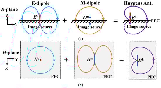
Figure 1.
Basic electric (E) and magnetic (H) field principles of a VP Huygens source antenna: (a) E-plane and (b) H-plane. Labels: E = electric, M = magnetic, H = Huygens.
Based on this operating principle, a two-port-fed VP HSA (Ant. I) was constructed. Its configuration is illustrated in Figure 2. The semi-circular loop is realized by the field of a cylindrical DR that is excited by a horizontal strip through port2, and the E-dipole is realized by the port1-excited monopole that is taken to be concentric with the DR. The radiated fields of this Ant. I were obtained by simultaneously exciting port1 and port2. Figure 3 presents its simulated S-parameters and radiation patterns. The overlapped −10 dB impedance bandwidth of |S11| and |S22| ranges from 1.77 to 1.98 GHz and the corresponding resonance frequency is 1.85 GHz yielding the FBW = 11.2%. It is highlighted with the blue background in Figure 3a. The corresponding profile, transverse size and ka are 0.15 λL, π × (0.14 λL)2, and 1.15, respectively, where λL is the wavelength of the lowest frequency in the impedance bandwidth. The E-plane and H-plane 2-D radiation patterns at the resonance frequency, 1.85 GHz, are shown Figure 3b,c. It is verified that Ant. I exhibits the expected unidirectional end-fire radiation pattern towards the +y-direction, which echoes well with the HSA principles illustrated in Figure 1.
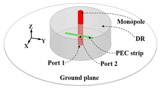
Figure 2.
DR-based VP HSA configuration.
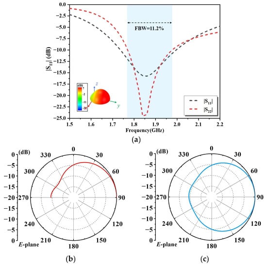
Figure 3.
Simulated responses of the DR-based VP HSA: (a) S-parameters; (b) Radiation patterns in the E-plane (yz-plane); and (c) H-plane (xy-plane) at the resonance frequency 1.85 GHz.
To gain further insight into the operating mechanism of this DR-based VP HSA, the horizontal-strip excited dielectric resonator antenna (DRA) and the monopole-excited DRA were analyzed separately. The model of the former is shown in Figure 4a. The simulated −10 dB impedance bandwidth ranged from 1.77 to 1.98 GHz with a resonance frequency of 1.85 GHz, i.e., a 11.2% fractional bandwidth (FBW). Figure 4b,c depict the E- and H-field distributions inside the cylindrical DR in the two principal vertical planes at that resonance frequency. It is noted that the DR encompasses a semicircular E-field in the yz-plane. The H-field is concentrated in its middle region and has the characteristic figure eight dipole pattern in the zx-plane. These field distributions are characteristic of its HEM11δ mode [19,24].
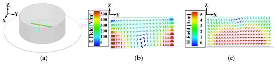
Figure 4.
Simulated model and field distributions of the horizontal-strip dipole excited DRA: (a) antenna configuration; (b) E-field on the yz-plane within the DRA; and (c) H-field on the zx-plane within the DRA.
The resonance frequency of a cylindrical DR operating in its HEM11δ mode is calculated with the empirical formulas [41]:
where c is the speed of light in free space. With εr, a and H denoting, respectively, the dielectric constant (10.0), radius (24.0 mm), and height (19.5 mm) of the cylindrical DR, they yield 1.81 GHz as the resonance frequency. This value agrees well with the simulated one, 1.85 GHz. Figure 5 shows the simulated radiation patterns in the yz-plane (E-plane) and xy-plane (H-plane). They indicate that this DRA radiates as a magnetic dipole oriented along the x-direction.
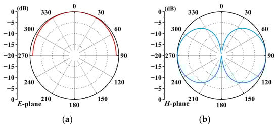
Figure 5.
Simulated radiation patterns of the horizontal dipole strip-excited DRA: (a) E-plane (yz-plane); (b) and H-plane (xy-plane).
The concentric monopole-excited DRA is displayed in Figure 6a. The height of the monopole was optimized to be 25.0 mm to make it operate at the same resonance frequency as the magnetic dipole, i.e., 1.85 GHz. Figure 6b,c display its simulated E-plane and H-plane radiation patterns. They clearly are those of an electric monopole, i.e., half of the dipole pattern in the yz-plane (E-plane) and omnidirectional in the xy-plane (H-plane).
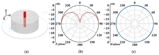
Figure 6.
Simulation model of the concentric-monopole excited DR antenna and its predicted radiation patterns: (a) configuration; (b) E-plane (yz-plane); and (c) H-plane (xy-plane).
2.2. Wideband DR-Based VP HSA
Because Ant. I required two ports to excite the E- and M-dipoles, it would be a cumbersome system in practice. Moreover, the height of the monopole results in its high profile. A single-port-fed DR-based VP HSA, Ant. II, that overcomes these drawbacks, is described next. The configuration of Ant. II is displayed in Figure 7. It consists of a DR and a 3D inverted-F antenna [42]. The DR is hollowed out by removing a small cylinder whose height is 6.5 mm and radius is 11.0 mm. The inverted-F structure is embedded into this hollow area.
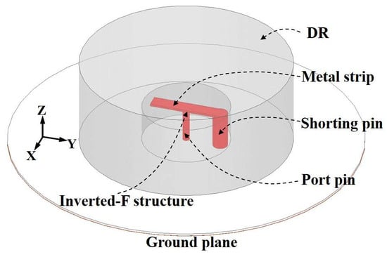
Figure 7.
Configuration of the single-port-fed wideband DR-based VP HSA.
The inverted-F antenna has several roles in this design. First, it acts as the electric dipole element that radiates a VP field. Second, it excites the DR’s HEM11δ mode to yield the M-dipole. Moreover, since it resides in the interior air-cylinder, its profile is significantly smaller than the monopole case in Figure 2 in which the monopole protrudes through the top of the DR. Third, the shorting pin regulates the phase difference between its electric and magnetic dipoles. When its distance along the y-axis from the port pin in the center of the DR is tuned properly, end-fire unidirectional fields are generated with their maxima being along the y-axis. The geometric structures of the resulting HSA and their corresponding radiation patterns are shown in Figure 8.
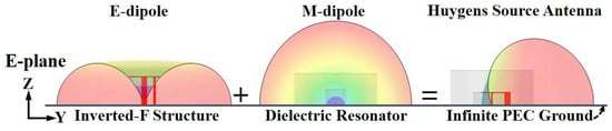
Figure 8.
The components of the single-port-fed wideband DR-based VP HSA together with their corresponding radiation patterns.
Figure 9 presents the simulated reflection coefficients of this DR-based VP HSA. The antenna exhibits two resonance frequencies located at 1.9 and 2.1 GHz. The first resonance is generated by the DR, and the second one is generated by the inverted-F antenna. The overlap of these two resonances forms a wide operating bandwidth ranging from 1.79 to 2.23 GHz, i.e., a FBW of 21.9%. This region is depicted with the blue shaded area in Figure 9. Similar unidirectional end-fire radiation patterns with their maxima being along the +y-direction are attained at its two resonance frequencies. While there are differences in their peak and antipodal values and beam-widths, they are relatively small. The antenna’s profile, transverse size, and ka are 0.12 λL, π (0.14 × λL)2 and 1.16, respectively. In comparison to Ant. I, the operating bandwidth of Ant. II is dramatically larger and its profile is smaller.
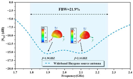
Figure 9.
Simulated reflection coefficient of the wideband HSA, Ant II, and the 3D-realized gain patterns at its two resonance frequencies.
2.3. Electrically Small DR-Based VP HSA
In order to further reduce the transverse size of Ant. II, a metal top-hat is introduced on the top of the DR. The configuration and simulated reflection coefficient (|S11|) values of the resulting miniaturized DR-based VP HSA, Ant. III, are shown in Figure 10. The latter are compared to those of Ant. I and Ant. II. The center frequency of Ant. III has been significantly red-shifted from 2.01 to 1.38 GHz when compared with that of Ant. II. Similarly, the overlap of its two resonance frequencies, i.e., 1.315 and 1.440 GHz, form a wide −10 dB impedance bandwidth ranging from 1.28 to 1.49 GHz, i.e., the FBW = 15.2%. The first and second resonances are generated by the top-hat loaded DR and the inverted-F antenna, respectively. The corresponding profile, transverse size, and ka are 0.083 λL, π × (0.10 λL)2 and 0.83, respectively. Note that Ant. III is electrically small and its profile is smaller than that of Ant. II.
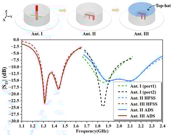
Figure 10.
Configurations and simulated |S11| values as functions of the source frequency for Ant. I, Ant. II, and Ant. III.
To fully explain the minimization effects in this design, an equivalent circuit model of Ant. III was developed. It is presented in Figure 11. The equivalent circuit of the driven element, i.e., the inverted-F structure, consists of the port pin and the metallic strip being represented as inductors (L1 and L2), and the shorting pin connected to the ground plane being modeled as a parallel capacitor, inductor, and resistor set (L3, C3, R1) [43]. The equivalent circuit of the parasitic elements, i.e., the DR and the top-hat, represents the DR as another parallel capacitor, inductor, and resistor set (L4, C4, R2), and the top-load patch as a tank circuit, i.e., a parallel capacitor–inductor pair (L5, C5) [22,44]. Furthermore, because the inverted-F structure transfers energy to the DR by means of a near-field capacitive-coupling effect, the capacitor, C1, is introduced to represent this effect. Finally, the top-hat patch in the presence of the ground plane introduces a capacitive load, which is denoted by C2 [22,44].
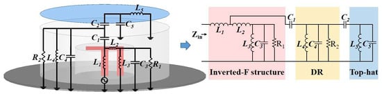
Figure 11.
The equivalent circuit model of Ant. III and the corresponding physical structures in it.
As illustrated in Figure 11, the equivalent circuit of Ant. III is composed of three parts, i.e., an inverted-F structure; a DR and its metallic top-hat; and the interacting capacitors (C1, C2). The equivalent circuit diagrams of the inverted-F structure, DR, and top-hat are marked with red, yellow, and blue shading in the circuit diagram, respectively. The values of the circuit of Ant. II are explicitly as follows: L1 = 1.37 nH, L2 = 2.9 nH, L3 = 1.35 nH, L4 = 1.798 nH, C1 = 0.693 pF, C3 = 4.7 pF, C4 = 2.84 pF, R1 = 68.7 Ω, and R2 = 117.3 Ω. Similarly, those of Ant. III are: L1 = 1.67 nH, L2 = 4.74 nH, L3 = 1.32 nH, L4 = 1.74 nH, L5 = 100.0 nH, C1 = 0.903 pF, C2 = 3.5 pF, C3 = 10.23 pF, C4 = 3.12 pF, R1 = 81.8 Ω, and R2 = 224.0 Ω.
The inverted-F structure and the DR exhibit two resonant frequencies at 2.1 and 1.9 GHz, respectively. With the addition of the interacting capacitor C1, these two resonances merge to give a wideband operation bandwidth that ranges from 1.79 to 2.23 GHz, as indicated by the solid blue line in Figure 10. These results also demonstrate that the dual resonances of Ant. II stem from the inverted-F structure and the DR. Furthermore, the top-hat is capacitive in the target frequency range. Thus, its presence and that of the interacting capacitor C2 downshifts the operating bandwidth of Ant. II to 1.28–1.49 GHz, as indicated by the red solid line in Figure 10. These results demonstrate that the top-hat loading in Ant. III leads to its miniaturization.
Figure 10 also plots the S-parameters calculated with this equivalent circuit in ADS for comparison with the HFSS-simulated responses of Ant. II and Ant. III. As Figure 10 indicates, the |S11| values of the equivalent circuit coincide quite well with those of the HFSS simulations. It is clearly shown that the operating frequency range red-shifted after the top-hat patch was introduced on the DR. The capacitor C2 nicely recovers its effects. The effective antenna miniaturization is thus explained.
3. Pattern-Reconfigurable Electrically Small DR-Based VP HSA
Because the inverted-F structure radiates a VP electric field, eed, the direction of the magnetic dipole moment, mmd, formed in the DR by its magnetic field exciting the HEM11δ mode, completely determines the peak direction of the unidirectional field radiated by the HSA, i.e., in the direction eed × mmd. Due to the structural symmetry of the cylindrical DR, the direction of the M-dipole moment could be conveniently adjusted in the azimuthal plane simply by rotating the inverted-F structure. This is illustrated clearly in Figure 12. State-1 is taken as an example. The E-dipole is along the +z-direction, and the M-dipole is along the +x-direction; they produce the unidirectional beam pointed in the +y-direction. Moreover, benefiting from the wide beamwidth character of the HSA, four pattern-reconfigurable states are sufficient to cover the entire azimuthal coverage, as shown in Figure 12b.
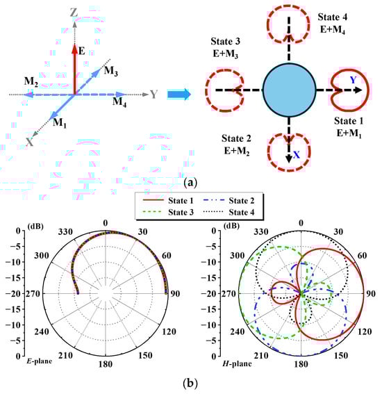
Figure 12.
Pattern-reconfigurable DR-based VP HAS: (a) working principle schematic diagrams; and (b) corresponding radiation patterns in the vertical planes (left) and horizontal plane (right).
Because the feed post is fixed at the origin, it is the location of the shorting pin of the inverted-F structure in the four cases in Figure 12 that adjusts the direction of the magnetic dipole moment. Consequently, the 3D inverted-F structure shown in Figure 13 was developed with four switchable states to realize the desired azimuthal pattern reconfigurability. Details of the configuration are given. The corresponding optimized design parameters are listed in Table 1.
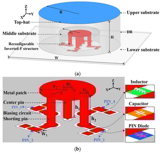
Figure 13.
Configuration of the pattern-reconfigurable DR-based VP ESA: (a) 3-D isometric view; and (b) its reconfigurable inverted-F structure.

Table 1.
Optimized design parameters of the developed ESA (in Millimeters).
Figure 13a illustrates that the pattern-reconfigurable DR-based VP ESA comprises three substrate boards, a cylindrical DR, and the reconfigurable 3D inverted -F structure. The ceramic material is alumina. Its dielectric constant εr and loss tangent tan δ are 10.0 and 0.018, respectively. The three boards are the copper-cladded substrate Rogers RT/duroid 5880 with a relative dielectric constant of εr = 2.2, loss tangent of tan δ = 0.0009, and copper cladding thickness of 0.018 mm. The thickness of their dielectric substrates are, respectively, 0.127, 0.787, and 0.508 mm from top to bottom. The top-hat patch with a radius of R is printed on the upper surface of the upper substrate, and the copper cladding on the lower surface of the lower substrate is utilized as the ground plane. An SMP connector was selected to feed the antenna.
The zoom-in view of the reconfigurable 3D inverted-F structure in Figure 13b reveals its details. It consists of a center pin, a metal patch, four shorting pins, and a reconfigurable biasing structure. The upper end of the center pin is connected to the center of the metal patch, and the lower end is connected to the inner conductor of the SMP connector. The upper ends of four shorting pins are connected to the edge of the metal patch and their lower ends are connected to the biasing structure. The biasing structure is composed of four pathways, which are printed in the slots etched in the ground plane. They are symmetrically arranged to accommodate the four switchable sectoral states. Each pathway contains a PIN diode, an RF choke inductor, a DC blocking capacitor, and several small metal pads for soldering the biasing lines. All four diodes are pin diodes [45]. These PIN diodes are represented in the simulations by a 0.8 Ω resistor in the ON state and a 0.2 pF capacitor in the OFF state, in correspondence with the data sheet of the employed MSWSE-050-17 PIN diodes. These four diodes are denoted as PIN_1, PIN_2, PIN_3, and PIN_4. All negative poles of these four diodes are connected to the ground plane, as depicted in Figure 13b. Four Murata 120 nH coil inductors were utilized to eliminate any adverse effects from the DC-biasing lines, and four Murata 3.3 pF capacitors were employed to avoid any occurrence of short-circuited DC currents and to realize independent control of the four pathways.
By controlling the ON/OFF state of the four PIN diodes, the orientation of the HEM11δ mode’s field distributions will change accordingly, and thereby the peak direction of the HSA’s unidirectional fields is dynamically switched. In particular, when PIN_1 is turned on, and PIN_2, PIN_3, and PIN_4 are turned off, the shorting pin located on the +y-axis is connected to the ground plane, leading to an inverted-F structure oriented along the +y-axis. As a consequence, the end-fire radiation pattern pointing along the +y-axis (State-1) is obtained. In a similar manner, when PIN_2, PIN_3, or PIN_4 is ON and the other three diodes are OFF, the end-fire radiation pattern points along the +x-axis (State-2), the −y-axis (State-3), and the −x-axis (State-3), respectively. These four pattern-reconfigurable states and the corresponding beam directions, together with their PIN diode states, are summarized in Table 2. By dynamically switching amongst these four pattern-reconfigurable states, the VP ESA achieves a 360° beam-scanning performance in its azimuthal plane.
Table 2.
Pin diodes states for the four pattern-reconfigurable states.
To further reveal the effects of each part of the antenna on its performance, several key parameter studies of the positions of the shorting pins, as well as the sizes of the top-hat and the ground plane, were performed. Due to the geometric symmetry of the antenna structure, it was only necessary to carry out parameter analyses with the antenna operating in State-1. Figure 14 illustrates the S-parameter values versus different distances (s) between the shorting pins and the medial axis. The data presented clearly indicate that the first resonance moves gradually towards lower frequencies as s increases from 5.7 to 6.7 mm. Thus, it leads to the deterioration of the overlapped impedance bandwidth. Consequently, the position of the shorting pins not only dictates the direction of the magnetic dipole moment, thereby determining the maximum radiation direction of the antenna—but it also plays a vital role in the impedance matching.
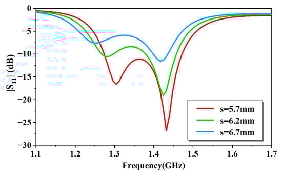
Figure 14.
Simulated |S11| curves for different positions of the shorting pins.
The simulation results of the antenna with varying sizes of the top-hat are illustrated in Figure 15. The diameter of the dielectric resonator was fixed at 24.0 mm, and only the size of the top-hat was altered. It is observed that increasing the top-hat size from 24.0 to 34.0 mm results in a redshift of the antenna’s entire bandwidth range by approximately 25 MHz. Additionally, the radiation patterns when the antenna is operating at its second resonance frequency are also presented. One finds that the tilt angle increases with an increase in the top-hat size. This phenomenon demonstrates an effective means of achieving larger tilt angles. Consequently, the size of the top-hat can be adjusted according to specific requirements in practical applications.
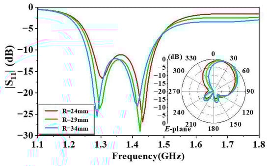
Figure 15.
Simulated |S11| values together with the radiation patterns at the second resonance frequency for different top-hat sizes.
The simulated performance of the antenna as its ground plane size varies is illustrated in Figure 16. One finds that the S-parameters of the antenna remain largely unchanged when the square ground plane side-length is 200, 250, and 300 mm. On the other hand, the tilt angle of the radiation beam increases from 20° to 35°, as it increases from 200 to 300 mm.
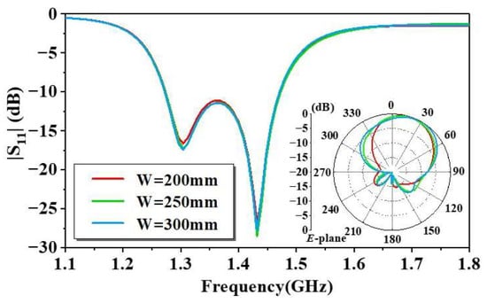
Figure 16.
Simulated |S11| values together with the radiation patterns at the second resonance frequency for different side-lengths of the square ground plane.
4. Experimental Validation
The optimized pattern-reconfigurable electrically small DR-based VP HSA was fabricated, assembled, and measured. There was a considerable savings in costs using a square aluminum plate with dimensions 0.85 λL × 0.85 λL rather than a Duroid sheet of the same size to simulate the large the ground plane. Because the plate was highly conductive and of similar extent to the ground plane in the simulation model shown in Figure 13, it had no noticeable impact on the measured results and, hence, on the comparisons with their simulated values. Photographs of the antenna under text (AUT) in the chamber and its components are exhibited in Figure 17. As shown in Figure 17a, the low-profile (0.085 λL) cylindrical DR with its top-hat is placed on the upper surface of a square piece of the lower dielectric substrate. The metallic reconfigurable inverted-F structure was 3D-printed; it is shown in Figure 17b. As depicted in Figure 17c, the DC biasing circuit was printed on the bottom surface of the square Duroid sheet, and five DC-biasing lines were located below the ground plane. They were utilized to control the ON/OFF states of the four PIN diodes. The four red wires were connected via the inductors to the positive poles of the four PIN diodes, and one blue wire was connected to the ground plane. Thus, each pattern state employed one corresponding red (“+” pole) line and the common blue (“−” pole) line.
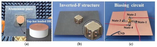
Figure 17.
Fabricated prototype. (a) AUT in the chamber; (b) reconfigurable 3D-inverted-F structure; And (c) state control structure with its DC biasing lines.
The measured |S11| results, together with their simulated values for each of the pattern-reconfigurable States 1–4, are presented in Figure 18. Note that the simulated curves in all four states exactly overlap due to the antenna’s symmetry. The simulated −10 dB impedance bandwidth in each state is 198 MHz, ranging from 1.274 to 1.472 GHz, which yields a broad FBW = 14.4%. The measured −10 dB impedance bandwidths (FBW) for State-1, State-2, State-3, and State-4 are, respectively, from 1.270 to 1.467 GHz (14.4%), from 1.268 to 1.468 GHz (14.6%), from 1.267 to 1.464 GHz (14.4%), and from 1.271 to 1.466 GHz (14.2%). Consequently, the measured overlapped −10 dB impedance bandwidth (FBW) for all four states is 193 MHz (14.1%), ranging from 1.271 to 1.464 GHz. Compared with the simulated results, there is a small error of 2% in the measured FBW. Overall, the measured and simulated values are in good agreement.
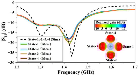
Figure 18.
Simulated and measured |S11| values together with the 3-D radiation patterns of the ES pattern-reconfigurable VP HSA in each of its four states.
The measured and simulated realized gain curves of all four pattern-reconfigurable states are presented in Figure 19a. The measured (simulated) peak realized gain (RG) is 6.07 dBi (6.5 dBi). Moreover, Figure 19b indicates that the measured (simulated) peak overall efficiency (OE) value was as high as 71.6% (77%). The discrepancy between the simulated and measured results are mainly due to the extra losses in the lumped circuit components and the relatively higher dielectric losses associated with the practical dielectric resonator material that we purchased in comparison to that employed in the simulations. The measured and simulated radiation patterns in each pattern-reconfigurable state at 1.4 GHz are presented in Figure 20. The measured results confirm that when the PIN states were changed, the main beam direction was steered towards opposite directions in the yz- and zx-planes, respectively, as predicted. Thus, the full 360° azimuthal beam steering ability was verified by the measurements. Moreover, the antenna exhibits a low cross-polarization level in each state, less than −30 dB. The measured and simulated radiation performance characteristics in each state of the developed pattern-reconfigurable DR-based VP HSA are summarized in Table 3.
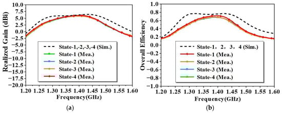
Figure 19.
The corresponding measured and simulated (a) realized gain and (b) OE values of the antenna in each of its four states.
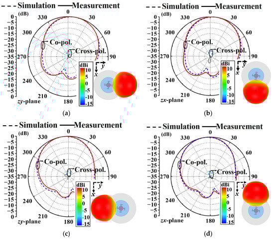
Figure 20.
The corresponding measured and simulated 2D and radiation patterns in each of its four states at 1.4 GHz: (a) State-1; (b) State-2; (c) State-3; and (d) State-4.
Table 3.
Performance characteristics of the electrically small pattern-configurable DR-based VP HSA.
5. Discussion
To demonstrate the advantages of the developed pattern-reconfigurable ES HSA, performance comparisons of its prototype with other previously reported Huygens DRAs are given in Table 4. Details include the DR’s dielectric constant, transverse electric size, profile, FBW, peak RG, pattern reconfigurability, and the antenna configuration. For a fair comparison, the electrical size and profile of each design is given with respect to the lower bound of its operational frequency range, i.e., λL. Moreover, we also scaled our design using the same materials, i.e., alumina ceramics with a dielectric constant of εr = 10.0 and Rogers 5880 substrate with a dielectric constant of εr = 2.2, to operate in a higher band similar to the comparison cases. The design with dimensions 0.22 λL × 0.22 λL and 0.065 λL achieves a 12% fractional bandwidth from 5.12 to 5.77 GHz with a maximum gain of 6.18 dBi.
Table 4.
Comparison of the pattern-configurable DR-based VP HSA with other related Huygens DRAs reported in the literature.
It is clear from this table that the developed antennas are comparable in size to the smallest ones but with the lowest profile. Moreover, it has the largest peak gain value of any of them and maintains a broad FBW. Particularly, the developed antenna possesses 360° beam coverage in entire azimuthal plane by dynamically switching among four pattern-reconfigurable states.
6. Conclusions
An ES, wideband, pattern-reconfigurable DR-based VP HSA was presented. It consists of an electronically reconfigurable inverted-F structure, a cylindrical DR with a metallic top-hat load, and a finite ground plane. The inverted-F structure not only serves as the low-profile E-dipole of the HSA, but it also acts as the excitation source that induces the orthogonal M-dipole, i.e., the HEM11δ mode of the DR. This antenna has four reconfigurable endfire states corresponding to four different 90° sectors. Its low profile and ES size are facilitated by the top-hat load. The experimental results confirmed its simulated performance characteristics. With its pattern-reconfigurability and VP properties, the developed HSA is a promising candidate for a variety of compact wireless communication and sensor systems that require long-distance operation and multi-user coverage for IoT applications.
Author Contributions
Conceptualization, R.W.Z.; methodology, Y.D., M.-C.T., M.L. and R.W.Z.; validation, Y.D.; writing—original draft preparation, Y.D.; writing—review and editing, Y.D., M.-C.T., M.L., Z.Z., Q.L. and R.W.Z. All authors have read and agreed to the published version of the manuscript.
Funding
This work was supported by the Graduate Research and Innovation Foundation of Chongqing (grant number CYB22067), the National Natural Science Foundation of China (grant numbers 62371080, 62031006, and 62425106), the Chongqing Natural Science Foundation (grant number CSTB2022NSCQ-LZX0015), and, in part, by New Chongqing Youth Innovation Talent Program (contract no. 2024NSCQ-qncxX0535).
Data Availability Statement
The original contributions presented in this study are included in the article. Further inquiries can be directed to the corresponding author(s).
Conflicts of Interest
The authors declare no conflict of interest.
Abbreviations
The following abbreviations are used in this manuscript:
| VP | Vertically polarized |
| ES | Electrically small |
| ESA | Electrically small antenna |
| HSA | Huygens source antenna |
| DR | Dielectric resonator |
| DRA | Dielectric resonator antenna |
| E-dipole | Electric dipole |
| M-dipole | Magnetic dipole |
| EAD | Egyptian axe dipole |
| CLL | Capacitively loaded loop |
| FBW | Fractional bandwidth |
| RG | Realized gain |
| Ant. | Antenna |
| Sim. | Simulation |
| Mea. | Measurement |
References
- Lin, W.; Ziolkowski, R.W. Theoretical analysis of beam-steerable, broadside-radiating Huygens dipole antenna arrays and experimental verification of an ultrathin prototype for wirelessly powered IoT applications. IEEE Open J. Antennas Propag. 2021, 2, 954–967. [Google Scholar] [CrossRef]
- Lee, S.-H.; Radha, S.M.; Shin, G.; Yoon, I.-J. Design of electrically small and thin Huygens source antenna. In Proceedings of the 2018 International Symposium on Antennas and Propagation (ISAP), Busan, Republic of Korea, 23–26 October 2018; pp. 1–2. [Google Scholar]
- Tang, M.-C.; Shi, T.; Ziolkowski, R.W. A study of 28 GHz, planar, multilayered, electrically small, broadside radiating, Huygens source antennas. IEEE Trans. Antennas Propag. 2017, 65, 6345–6354. [Google Scholar] [CrossRef]
- Lin, W.; Ziolkowski, R.W. Electrically-small rectenna with Huygens radiation pattern for wireless power transfer applications. In Proceedings of the 2018 IEEE International Symposium on Antennas and Propagation & USNC/URSI National Radio Science Meeting, Boston, MA, USA, 8–13 July 2018; pp. 311–312. [Google Scholar]
- Tang, M.-C.; Wang, H.; Ziolkowski, R.W. Design and testing of simple, electrically small, low-profile, Huygens source antennas with broadside radiation performance. IEEE Trans. Antennas Propag. 2016, 64, 4607–4617. [Google Scholar] [CrossRef]
- Lin, W.; Ziolkowski, R.W. Electrically small, low-profile, Huygens circularly polarized antenna. IEEE Trans. Antennas Propag. 2018, 66, 636–643. [Google Scholar] [CrossRef]
- Wu, Z.; Tang, M.-C.; Shi, T.; Ziolkowski, R.W. Two-port, dual-circularly polarized, low-profile broadside-radiating electrically small Huygens dipole antenna. IEEE Trans. Antennas Propag. 2021, 69, 514–519. [Google Scholar] [CrossRef]
- Wu, Z.; Tang, M.-C.; Ziolkowski, R.W. Broadside radiating, low-profile, electrically small, Huygens dipole filtenna. IEEE Antennas Wireless Propag. Lett. 2022, 21, 556–560. [Google Scholar] [CrossRef]
- Tang, M.-C.; Wu, Z.; Shi, T.; Zeng, H.; Lin, W.; Ziolkowski, R.W. Dual-linearly polarized, electrically small, low-profile, broadside radiating, Huygens dipole antenna. IEEE Trans. Antennas Propag. 2018, 66, 3877–3885. [Google Scholar] [CrossRef]
- Yin, X.; Chen, S.J.; Fumeaux, C. A Huygens source quasi-end-fire button antenna. In Proceedings of the 2023 5th Australian Microwave Symposium (AMS), Melbourne, Australia, 16–17 February 2023; pp. 9–10. [Google Scholar]
- Lee, S.-H.; Shin, G.; Radha, S.M.; Choi, J.-Y.; Yoon, I.-J. Low-profile, electrically small planar Huygens source antenna with an endfire radiation characteristic. IEEE Antennas Wireless Propag. Lett. 2019, 18, 412–416. [Google Scholar] [CrossRef]
- Tang, M.-C.; Zhou, B.; Ziolkowski, R.W. Low-profile, electrically small, Huygens source antenna with pattern-reconfigurability that covers the entire azimuthal plane. IEEE Trans. Antennas Propag. 2017, 65, 1063–1072. [Google Scholar] [CrossRef]
- Best, S.R. Progress in the design and realization of an electrically small Huygens source. In Proceedings of the 2010 International Workshop on Antenna Technology (iWAT), Lisbon, Portugal, 1–3 March 2010; pp. 1–4. [Google Scholar]
- Huang, H.-F.; Bu, H.-L. Single-layer electrically small antenna with reconfigurable radiation pattern. In Proceedings of the 2021 IEEE MTT-S International Wireless Symposium (IWS), Nanjing, China, 23–26 May 2021; pp. 1–3. [Google Scholar]
- Wu, Z.; Tang, M.-C.; Ziolkowski, R.W. Electrically small, planar, frequency-agile, beam-switchable Huygens dipole antenna. IEEE Trans. Antennas Propag. 2021, 69, 8271–8281. [Google Scholar] [CrossRef]
- Pfeiffer, C.; Grbic, A. Realizing Huygens sources through spherical sheet impedances. In Proceedings of the 2012 IEEE International Symposium on Antennas and Propagation, Chicago, IL, USA, 8–14 July 2012; pp. 1–2. [Google Scholar]
- Wei, K.; Zhang, Z.; Feng, Z. Design of a wideband horizontally polarized omnidirectional printed loop antenna. IEEE Antennas Wireless Propag. Lett. 2012, 11, 49–52. [Google Scholar]
- Chen, X.; Tang, M.-C.; Yi, D.; Ziolkowski, R.W. Wideband, compact antennas with interdigitated magnetic-based near-field resonant parasitic elements. IEEE Trans. Antennas Propag. 2021, 69, 5036–5041. [Google Scholar] [CrossRef]
- Guo, L.; Leung, K.W.; Pan, Y.M. Compact unidirectional ring dielectric resonator antennas with lateral radiation. IEEE Trans. Antennas Propag. 2015, 63, 5334–5342. [Google Scholar] [CrossRef]
- Morales, C.D.; Morlaas, C.; Chabory, A.; Pascaud, R.; Grzeskowiak, M.; Mazingue, G. Huygens source antenna using stacked dielectric resonators. In Proceedings of the 2020 IEEE International Symposium on Antennas and Propagation and North American Radio Science Meeting, Montreal, QC, Canada, 5–10 July 2020; pp. 105–106. [Google Scholar]
- Jacobsen, R.E.; Lavrinenko, A.V.; Arslanagić, S. A water-based Huygens dielectric resonator antenna. IEEE Open J. Antennas Propag. 2020, 1, 493–499. [Google Scholar] [CrossRef]
- Wang, Z.; Dong, Y.; Peng, Z.; Hong, W. Hybrid metasurface, dielectric resonator, low-cost, wide-angle beam-scanning antenna for 5G base station application. IEEE Trans. Antennas Propag. 2022, 70, 7646–7658. [Google Scholar] [CrossRef]
- Ma, B.; Pan, J.; Huang, S.; Yang, D.; Guo, Y.-X. Unidirectional dielectric resonator antennas employing electric and magnetic dipole moments. IEEE Trans. Antennas Propag. 2021, 69, 6918–6923. [Google Scholar]
- Guo, L.; Leung, K.W. Compact linearly and circularly polarized unidirectional dielectric resonator antennas. IEEE Trans. Antennas Propag. 2016, 64, 2067–2074. [Google Scholar] [CrossRef]
- Pan, Y.M.; Leung, K.W.; Guo, L. Compact laterally radiating dielectric resonator antenna with small ground plane. IEEE Trans. Antennas Propag. 2017, 65, 4305–4310. [Google Scholar] [CrossRef]
- Guo, L.; Leung, K.W.; Yang, N. Wide-beamwidth unilateral dielectric resonator antenna using higher-order mode. IEEE Antennas Wireless Propag. 2019, 18, 93–97. [Google Scholar] [CrossRef]
- Guo, L.; Leung, K.W. Compact unilateral circularly polarized dielectric resonator antenna. IEEE Trans. Antennas Propag. 2018, 66, 668–674. [Google Scholar] [CrossRef]
- Wang, Z.; Zhao, S.; Dong, Y. Metamaterial-based wide-beam dielectric resonator antenna for broadband wide-angle beam-scanning phased array applications. IEEE Trans. Antennas Propag. 2022, 70, 9061–9072. [Google Scholar] [CrossRef]
- Wang, Z.; Zhao, S.; Dong, Y. Miniaturized, vertically polarized, pattern reconfigurable dielectric resonator antenna and its phased array for wide-angle beam steering. IEEE Trans. Antennas Propag. 2022, 70, 9233–9246. [Google Scholar] [CrossRef]
- Pan, Y.-M. A complementary dielectric resonator antenna with uniform hemispherical radiation. In Proceedings of the 2018 International Applied Computational Electromagnetics Society Symposium-China (ACES), Beijing, China, 29 July–1 August 2018; pp. 1–2. [Google Scholar]
- Han, S.; Wang, Z.; Dong, Y. Dielectric resonator antenna with reconfigurable patterns based on Huygens source. In Proceedings of the 2024 International Conference on Microwave and Millimeter Wave Technology (ICMMT), Bejing, China, 16–19 May 2024; pp. 1–3. [Google Scholar]
- Han, S.; Wang, Z.; Dong, Y. Planar beam-steering dielectric resonator antenna based on hybrid excitation method. IEEE Antennas Wireless Propag. 2024, 23, 3609–3613. [Google Scholar] [CrossRef]
- Wang, Z.; Dong, Y. Theory, design, and verification of miniaturized phase-controlled Huygens antenna for 360° continuous beam scanning. IEEE Trans. Antennas Propag. 2023, 70, 3104–3113. [Google Scholar] [CrossRef]
- Song, W.; Weng, Z.; Jiao, Y.-C.; Wang, L.; Yu, H.-W. Omnidirectional WLAN antenna with common-mode current suppression. IEEE Trans. Antennas Propag. 2021, 69, 5980–5985. [Google Scholar] [CrossRef]
- Qin, Y.; Zhang, L.; Mao, C.; Zhu, H. Low-profile compact tri-band multimode reconfigurable antenna using characteristic mode analysis. IEEE Trans. Antennas Propag. 2023, 7, 6144–6149. [Google Scholar] [CrossRef]
- Artner, G.; Kotterman, W.; Galdo, G.D.; Hein, M.A. Conformal automotive roof-top antenna cavity with increased coverage to vulnerable road users. IEEE Antennas Wireless Propag. 2018, 17, 2399–2403. [Google Scholar] [CrossRef]
- Tang, M.-C.; Duan, Y.; Wu, Z.; Chen, X.; Li, M.; Ziolkowski, R.W. Pattern reconfigurable, vertically polarized, low-profile, compact, near-field resonant parasitic antenna. IEEE Trans. Antennas Propag. 2019, 67, 1467–1475. [Google Scholar] [CrossRef]
- Wang, Z.; Liu, S.; Dong, Y. A compact, broadband, monopole-like endfire antenna with reconfigurable patterns for 5G applications. IEEE Trans. Antennas Propag. 2022, 70, 7199–7204. [Google Scholar] [CrossRef]
- Chen, S.-L.; Qin, P.-Y.; Lin, W.; Guo, Y.J. Pattern-reconfigurable antenna with five switchable beams in elevation plane. IEEE Antennas Wireless Propag. 2018, 17, 454–457. [Google Scholar] [CrossRef]
- Zhao, S.; Wang, Z.; Dong, Y. Pattern-reconfigurable antenna using low-profile electric and magnetic radiators. IEEE Antennas Wireless Propag. 2023, 22, 616–620. [Google Scholar] [CrossRef]
- Mongia, R.K.; Bhartia, P. Dielectric resonator antennas—A review and general design relations for resonant frequency and bandwidth. Int. J. Microw. Millim.-Wave Comput.-Aided Eng. 1994, 4, 230–247. [Google Scholar] [CrossRef]
- Fu, Y.; Huang, C.; Gao, C.; Liang, Y. Study on inverted F-shaped RFID antenna. In Proceedings of the 2020 21st International Conference on Electronic Packaging Technology (ICEPT), Guangzhou, China, 12–15 August 2020; pp. 1–4. [Google Scholar]
- Duan, Y.; Tang, M.-C.; Wu, Z.; Zhang, Z.; Yi, D.; Li, M. Omnidirectional-radiating, vertically polarized, wideband, electrically small filtenna. IEEE Trans. Circuits Syst. II, Exp. Briefs 2023, 70, 1380–1384. [Google Scholar] [CrossRef]
- Zhao, S.-K.; Liu, N.-W.; Chen, Q.; Fu, G.; Chen, X.-P. A low-profile dielectric resonator antenna with compact-size and wide bandwidth by using metasurface. IEEE Access 2021, 9, 29819–29826. [Google Scholar] [CrossRef]
- MACOM. Products: MSWSE-050-17. Available online: https://cdn.macom.com/datasheets/MSWSE-050-17.pdf (accessed on 5 February 2025).
Disclaimer/Publisher’s Note: The statements, opinions and data contained in all publications are solely those of the individual author(s) and contributor(s) and not of MDPI and/or the editor(s). MDPI and/or the editor(s) disclaim responsibility for any injury to people or property resulting from any ideas, methods, instructions or products referred to in the content. |
© 2025 by the authors. Licensee MDPI, Basel, Switzerland. This article is an open access article distributed under the terms and conditions of the Creative Commons Attribution (CC BY) license (https://creativecommons.org/licenses/by/4.0/).