Article

Enhanced Monte Carlo Simulations for Electron Energy Loss Mitigation in Real-Space Nanoimaging of Thick Biological Samples and Microchips

1
Brookhaven National Laboratory, National Synchrotron Light Source II, Upton, NY 11973, USA
2
Laboratory for BioMolecular Structure, Brookhaven National Laboratory, Upton, NY 11973, USA
*
Author to whom correspondence should be addressed.
Electronics 2025, 14(3), 469; https://doi.org/10.3390/electronics14030469
Submission received: 15 December 2024 / Revised: 9 January 2025 / Accepted: 22 January 2025 / Published: 24 January 2025

Abstract

:
High-resolution imaging using Transmission Electron Microscopy (TEM) is essential for applications such as grain boundary analysis, microchip defect characterization, and biological imaging. However, TEM images are often compromised by electron energy spread and other factors. In TEM mode, where the objective and projector lenses are positioned downstream of the sample, electron–sample interactions cause energy loss, which adversely impacts image quality and resolution. This study introduces a simulation tool to estimate the electron energy loss spectrum (EELS) as a function of sample thickness, covering electron beam energies from 300 keV to 3 MeV. Leveraging recent advances in MeV-TEM/STEM technology, which includes a state-of-the-art electron source with 2-picometer emittance, an energy spread of 3 × 10 5 , and optimized beam characteristics, we aim to minimize energy spread. By integrating EELS capabilities into the BNL Monte Carlo (MC) simulation code for thicker samples, we evaluate electron beam parameters to mitigate energy spread resulting from electron–sample interactions. Based on our simulations, we propose an experimental procedure for quantitively distinguishing between elastic and inelastic scattering. The findings will guide the selection of optimal beam settings, thereby enhancing resolution for nanoimaging of thick biological samples and microchips.

1. Introduction

The permissible thickness of a sample in electron microscopy is governed by both the electron beam energy and the underlying mechanisms of image formation. Advanced techniques, such as cryo-electron microscopy (cryo-EM) and cryo-electron tomography (cryo-ET) [1,2,3,4], widely employed in biological research, often rely on the Weak Phase Object Approximation (WPOA) to reconstruct the sample’s projected electrostatic potential from the exit electron wave function. In this framework, images are primarily generated through the coherent interference of elastically scattered electrons, a process known as phase contrast. However, phase contrast is highly sensitive to factors such as defocus, spherical and chromatic aberrations, objective aperture size, and illumination conditions, all of which collectively influence spatial resolution and image quality.
Inelastic scattering, which occurs when electrons lose energy during interactions with the sample, contributes to background noise and reduces the signal-to-noise ratio (SNR). For thin samples, resolution is mainly limited by elastic scattering and associated aberrations, with inelastic scattering having a minimal impact. As sample thickness increases, however, inelastic scattering becomes more significant, leading to increased energy loss and further degradation of resolution.
For thicker samples, the interplay between sample thickness, spatial resolution and image quality becomes increasingly complex due to the occurrence of multiple scattering events. At electron energies above a few MeVs, the assumptions underlying conventional low-energy TEM, which is primarily used for thin, sub-micrometer samples, are no longer valid. This necessitates the application of advanced models to optimize imaging performance under high-energy conditions. Spatial resolution, as a purely technical measure of the smallest distinguishable feature size, depends on several factors, including the wavelength of the electrons (determined by the accelerating voltage of the microscope), lens aberrations, instrument stability, and detector properties. However, image quality encompasses additional information, such as contrast, noise, and overall clarity. Consequently, high spatial resolution does not inherently ensure high image quality, as noise, artifacts, or poor contrast can obscure the image. Conversely, good image quality can sometimes be achieved even with moderate resolution if contrast and signal-to-noise ratio are optimized. While higher electron energies reduce the relative contribution of inelastic scattering to total energy loss, they also influence factors such as energy spread and chromatic aberration, which in turn affect image resolution as well as image quality [5,6]. Addressing this issue is inherently complex (briefly discussed in Appendix A.1 in the Appendix A) and, in this manuscript, we specifically focus on numerically estimating how energy loss varies with electron beam energy and sample thickness.
To address these challenges, we have developed an innovative tool within the BNL-MC simulation code [7] to model the electron energy loss spectrum (EELS) as a function of both sample thickness and electron beam energy (Figure 1). Our simulations demonstrate that, for thick samples, up to 15 μm, and an electron energy of 3 MeV, the energy loss resulting from electron–sample interactions leads to a normalized energy spread that is significantly lower than at an electron energy of 300 keV, on the order of a few ×10−4. We expect this value to decrease further with an increase in electron beam energy, which will be the focus of our future studies. The primary objective of this study is to optimize electron beam parameters in MeV-TEM/STEM, with a particular focus on minimizing energy spread. By leveraging the newly developed EELS simulation tool, integrated with the enhanced BNL Monte Carlo (MC) code, we aim to identify optimal electron beam settings for a broad range of applications. These include studying biological macromolecules, such as proteins and viruses, where high resolution is critical for observing molecular structures, and inspecting microchips and advanced materials, where precision imaging is essential for defect detection and material characterization. Our simulations will predict the effects of various parameters on image quality, enabling fine-tuning of beam settings to meet the specific requirements of each application. This work represents a significant advancement in improving the resolution and capabilities of high-energy electron microscopy, with broad implications for molecular biology, drug development, and materials science by reducing energy loss during electron–sample interactions. Especially in drug development, the ability to image thick biological samples in their native state allows for high-resolution visualization of complex macromolecules, such as proteins and nucleic acids, as well as their interactions with drug candidates. This capability offers detailed structural insights into molecular mechanisms, including protein conformational changes, binding dynamics, and the identification of key drug-target interactions. Such precision not only accelerates the drug discovery process but also aids in the rational design of more effective, targeted therapeutics.
Furthermore, based on our simulations, we propose an experimental procedure designed to quantitatively distinguish between elastic and inelastic scattering events. This procedure aims to provide a more accurate understanding of scattering mechanisms in electron microscopy, which is essential for improving both the precision of imaging and the interpretation of complex sample interactions.

2. Results

2.1. Implementing MC Simulation with EELS Capability

The electron beam profile was generated using state-of-the-art parameters: a 2 pm geometrical emittance, a 3 × 10 5 normalized energy spread ( σ E E ) that is dimensionless, and optimized chromatic (1.8 cm) and spherical (16 cm) aberrations of the objective lens [5,8,9] and listed in Table 1. This compact, ultra-high-brightness MeV electron source is achieved through the optimization of both emittance and energy spread from the photoinjector [5]. The optimization process involves fine-tuning key parameters, such as laser duration, transverse size, and the amplitude and phase of the accelerating fields. By minimizing energy jitters induced by fluctuations in the amplitude and phase stability of the accelerating fields, the energy spread is significantly reduced. This results in a substantially smaller energy spread, especially when the bunch charge is reduced to a single electron per pulse, effectively eliminating space charge effects and improving the overall performance of the MeV electron source.
The initial distribution used in the MC simulations had an RMS (root-mean-square) beam size of 1 nm, a convergence semi-angle of 1 mrad at the focal position, and a total of 10,000 electrons. For each simulation step, an electron was randomly selected from this distribution. Each event, whether elastic (channel 1, denoted c1), inelastic (c2), or no scattering (c3), was chosen probabilistically based on the event’s likelihood over the sample thickness, d t (set to 0.5 nm), as described by Equations (1) and (2):
σ e l h 2 c 2 Z 4 3 π E 0 2 β 2 ,   β 2 = 1 E 0 E + E 0 2
σ i n e l 1.5 × 10 6 Z 1 2 β 2 ln ( 2 θ c ) ,   θ c = Δ E β 2 ( E + E 0 )
The total inelastic scattering cross-section ( σ i n e l ) was scaled to three times the total elastic scattering cross-section ( σ e l ) , with R i n 2 e l 3 [10,11], consistent with values reported by Dr. Henderson [12] and Peet et al. [13] for 500 KeV electrons, without considering high voltage effects on the ratio. When an electron interacts with the specimen, the probability of undergoing event i (elastic or inelastic scattering) within a sample thickness dt is given by
P = σ i ρ d t = K i d t
where σ i is the cross-section for event i, ρ is the sample density, and K i is the scattering coefficient. The density of amorphous ice (0.92 g/cm3), as used by Langmore and Smith [14] and Jacobsen et al. [15], was applied in the simulation. The scattering angle for each event was determined based on the differential scattering cross-section for each angle interval (dθ) for both elastic (Equation (4)) and inelastic (Equation (5)) scattering.
d σ e l d Ω = 2 Z R 2 1 + E E 0 a H ( 1 + ( θ θ e l ) 2 ) 2 ,   θ e l = λ 2 π R , R = a H Z 1 3
d σ i n e l d Ω Z λ 4 1 + E E 0 2 4 π 2 a H 2 1 1 + θ 0 2 + θ 2 θ 0 2 2 θ 2 + θ E 2 2 ,   θ E = E E E + E 0 E + 2 E 0
For elastic scattering, the cross-section for each angle interval is the sum of the oxygen ( σ O _ a t o m ) and hydrogen ( σ H _ a t o m ) cross-sections, as σ i c e = σ O _ a t o m + 2 σ H _ a t o m . For inelastic scattering, the cross-section is set to 110% of the oxygen cross-section [11]. The cross-sections of oxygen in amorphous ice are calculated using Equations (1), (2), (4) and (5), and listed in Table 2. The angle interval dθ is defined with varying values to maintain a nearly constant probability density: 0.001 mrad for θ less than 0.6 mrad, 0.01 mrad for θ less than 6.3 mrad, 0.1 mrad for θ less than 67 mrad, 1 mrad for θ less than 600 mrad, and 10 mrad for larger θ values. The electron’s position was updated based on the scattering angle and the distance dt along the scattering direction, while the event type was recorded. The procedure was repeated, e.g., for a 15 μm thick sample, resulting in 30,000 iterations (15 μm/dt).
The original MC code categorizes each electron at depth t into one of five groups: no scattering, single elastic scattering, multiple elastic scattering, at least one inelastic scattering, or scattered outside the detector collection angles [14,15,16]. The BNL-MC code extends this approach by retaining the scattering event labels for each electron as it traverses each sample layer, ensuring consistency across the distribution.
For each layer of thickness dt, an event, whether elastic scattering (c1), inelastic scattering (c2), or no scattering (c3), is selected based on the probabilities associated with each event. As the electron traverses the sample, it is assigned to one of these identities (c1, c2, or c3) for each layer. The EELS is then determined through MC simulation using the BNL-MC code. For each electron, the number of inelastic scattering events is counted, and the inelastic scattering frequency is determined as a function of sample thickness. This process is repeated for all electrons in the distribution to generate a histogram of inelastic scattering events at a specific thickness. Histograms at various sample thicknesses then yield the EELS.
The mean energy loss (MEL), or stopping power, represents the energy lost by an electron during an inelastic scattering event. This experimentally determined quantity is essential for calculating inelastic cross-sections and, consequently, the EELS. For a 300 keV electron in amorphous ice, the measured MEL is 39.3 eV [10,17].
The energy loss of an electron is described by the Bethe–Bloch formula (Equation (6)) [10,18]
d E d t = 4 π N A r e 2 m e c 2 l n 2 m e c 2 β 2 I β 2 β 2 = 4 π N A r e 2 m e c 2 · f ( E )
which represents the rate of energy loss due to ionization, depending on the electron’s velocity and the material’s properties. Here, N A , r e , m e , c, β , and I are Avogadro’s number, the classical electron radius, the electron mass, the speed of light, the electron’s velocity as a fraction of the speed of light, and the material’s mean excitation energy, respectively. Energy dependence is reflected in the relativistic β -term, as shown in Equation (7):
f E = l n 2 m e c 2 β 2 I β 2 / β 2
Using the Bethe–Bloch formula and the experimentally measured MEL of 39.3 eV for a 300 keV electron in amorphous ice, along with the calculated mean free path (MFP) for different electron beam energies (Figure 2) [5,6], we can derive MEL for various electron beam energies. This relationship is expressed as
M E L E = d E d t · M F P
where d E d t = d E 0 d t · f ( E ) f ( E 0 ) , ( E 0 = 300   keV ) . Ianik Pante [19] has extensively studied the behavior of elastic and inelastic scattering cross-sections, finding that both decrease as the electron energy increases. However, these cross-sections gradually approach saturation for electron energies exceeding 1 MeV, with an MFP approximately equal to 0.5 μm (as shown in Figure 2 for inelastic scattering).
For example, using Equation (8), the MEL for a 3 MeV electron is calculated to be 102.8 eV. This method can be similarly applied to calculate MEL for other electron energies.

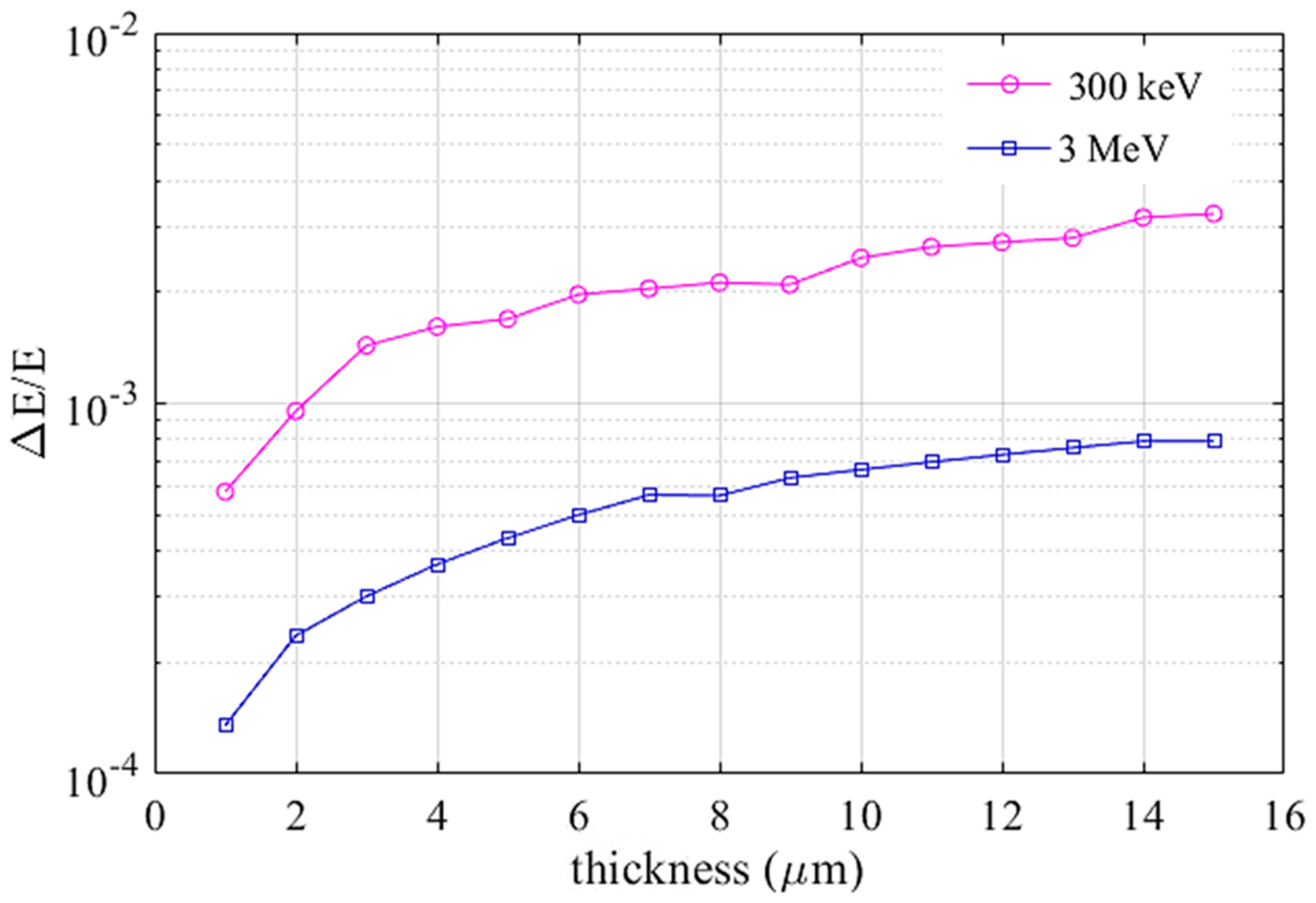
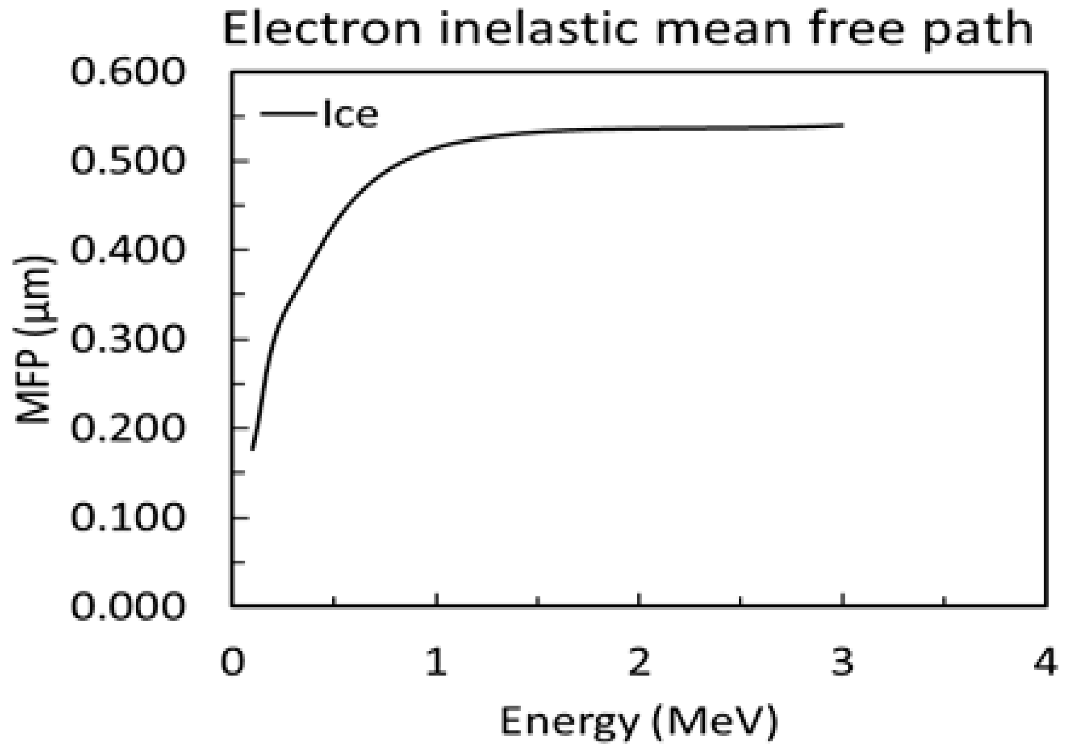
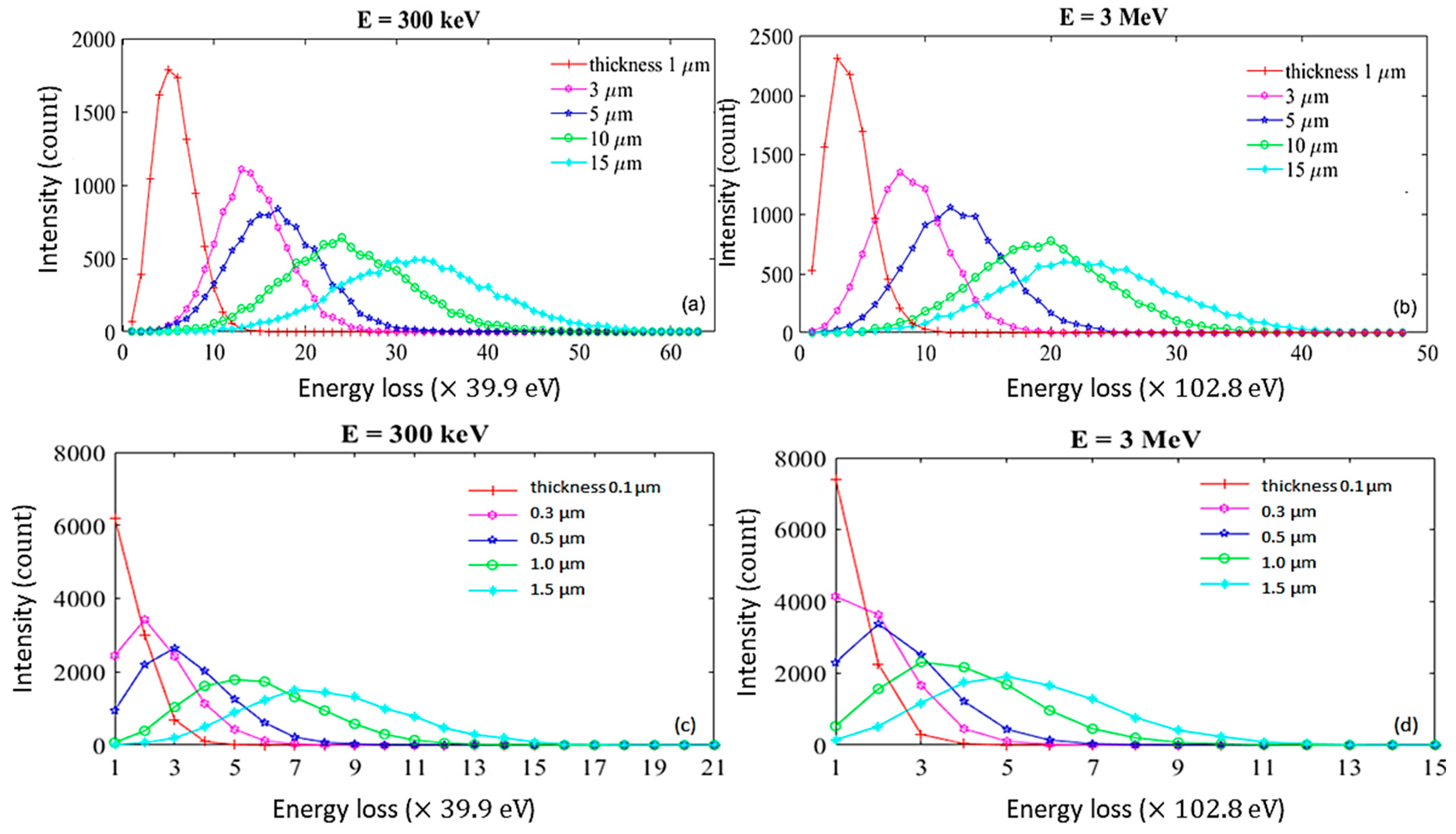
2.2. Simulating EELS

EELS is simulated using the BNL-MC code. For each electron passing through multiple layers of the sample, the number of inelastic scattering events is recorded, providing the count of such events as a function of sample thickness. This process is repeated for all electrons in the distribution, generating histograms of inelastic scattering events at each sample thickness with a step size of 0.5 nm. These histograms correspond to the electron energy loss spectra, as shown in Figure 3a,b for sample thickness up to 15 μm, and in Figure 3c,d for a thin sample with thickness ranging from 0–1.5 μm. The energy loss, in units of electron volts (eV), is obtained by multiplying the values on the horizontal axis by M E L = 39.9   e V for 300 keV and M E L = 102.8   e V for 3 MeV. Therefore, in the manuscript, we label the corresponding axis as energy loss in units of MEL regarding the electron beam energy per inelastic scattering event.

2.3. Analyzing EELS via Two Methods

Two methods are employed to estimate energy loss as a function of sample thickness from the simulated EELS data.

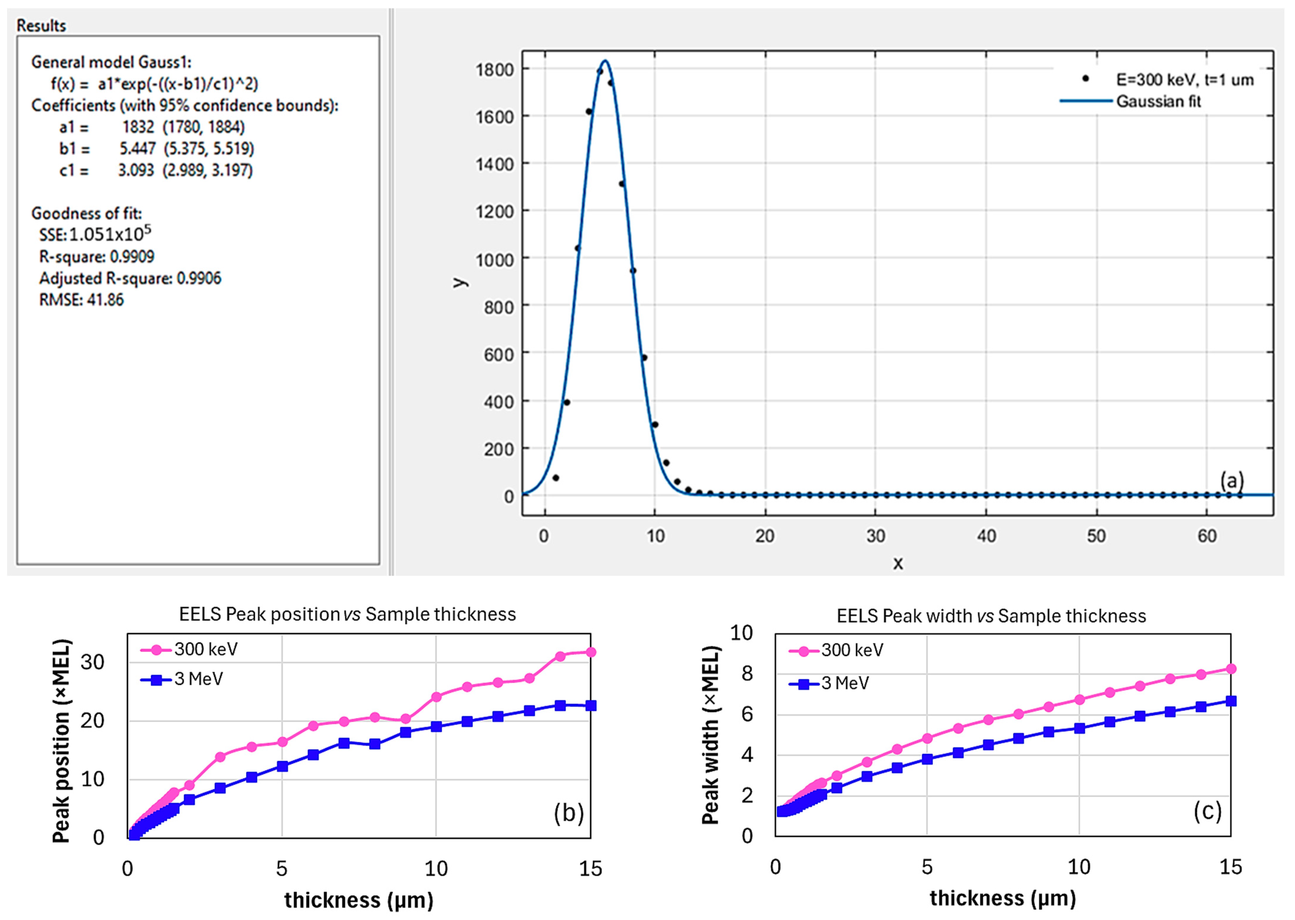
2.3.1. Method 1: Gaussian Fitting

Gaussian fitting is applied to each EELS curve, as in the example shown in Figure 4a for a 1 μm thick sample. This technique allows for the extraction of key parameters, such as the peak position, width, and amplitude. The peak position represents the average energy loss and is used to estimate energy loss in units of MEL per inelastic scattering event. This approach is referred to as the Gaussian Fit EELS (GF-EELS) method. Figure 4b–d shows the peak positions, widths, and amplitudes obtained from applying the GF-EELS method to the EELS curves in Figure 3a,b.

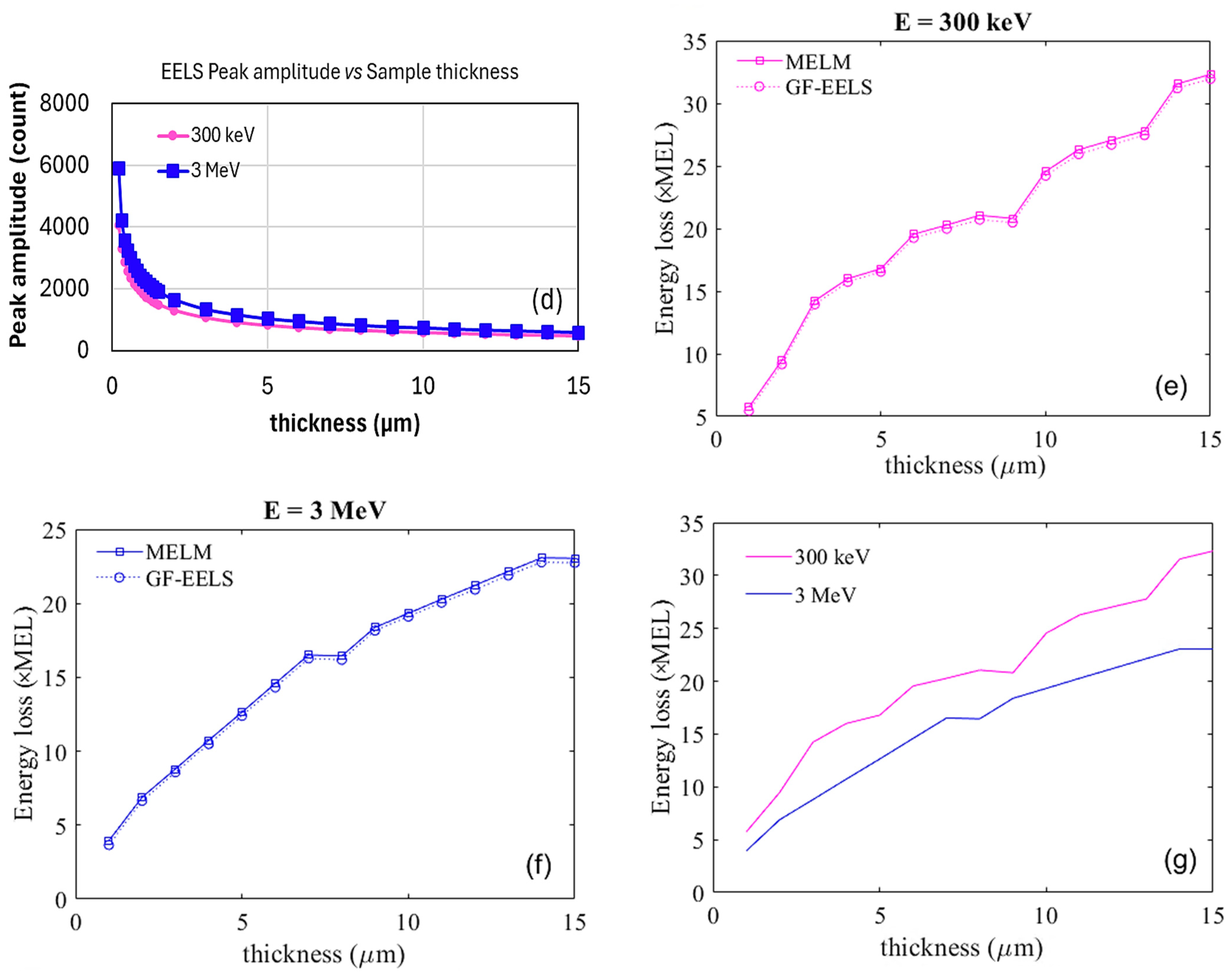
2.3.2. Method 2: Analytical Estimation of Energy Loss

Alternatively, the mean energy loss for each EELS can be calculated by integrating energy loss distribution, as described in Equation (9) [20]. This method, called the Mean Energy Loss Method (MELM), provides a quantitative measure of the average energy lost by electrons due to inelastic scattering. Unlike the GF-EELS method, which estimates the mean energy loss based on the EELS peak position, MELM takes into account the entire energy loss distribution, making it more robust, especially when the spectral shape deviates from Gaussian. MELM is also more reliable when the EELS peak is near zero energy loss, where Gaussian fitting can introduce significant errors.
Δ E = 0 Δ E I i n e l d Δ E 0 I i n e l d Δ E
Energy loss is analyzed using two methods: GF-EELS (dashed lines) and MELM (solid lines). These two methods are equivalent when the EELS curve follows a Gaussian distribution. A detailed mathematical derivation of their equivalence is provided in Appendix A.2 of the Appendix A. Energy losses as a function of sample thickness are shown in Figure 4e,f for two electron beam energies: (e) 300 keV and (f) 3 MeV. Figure 4g displays the energy loss estimated using MELM for 300 keV (magenta) and 3 MeV (blue). The vertical axis represents the energy loss in units of MEL per inelastic scattering event, which varies strongly with electron beam energy.
Energy loss exhibits nonlinear behavior as a function of sample thickness when the thickness exceeds 1.9 μm for 300 keV and 2.9 μm for 3 MeV, as illustrated in Figure 4b,g, with further details provided in Section 2.4. At these electron beam energies, the critical angles for both elastic and inelastic scattering are significantly large, on the order of several milliradians or more, as observed in MeV-STEM studies [5,6] and shown in Table 2. This increases the likelihood of large angle scattering events, leading to longer effective electron path lengths and resulting in deviations from energy loss predictions that are based solely on sample thickness and MFP.

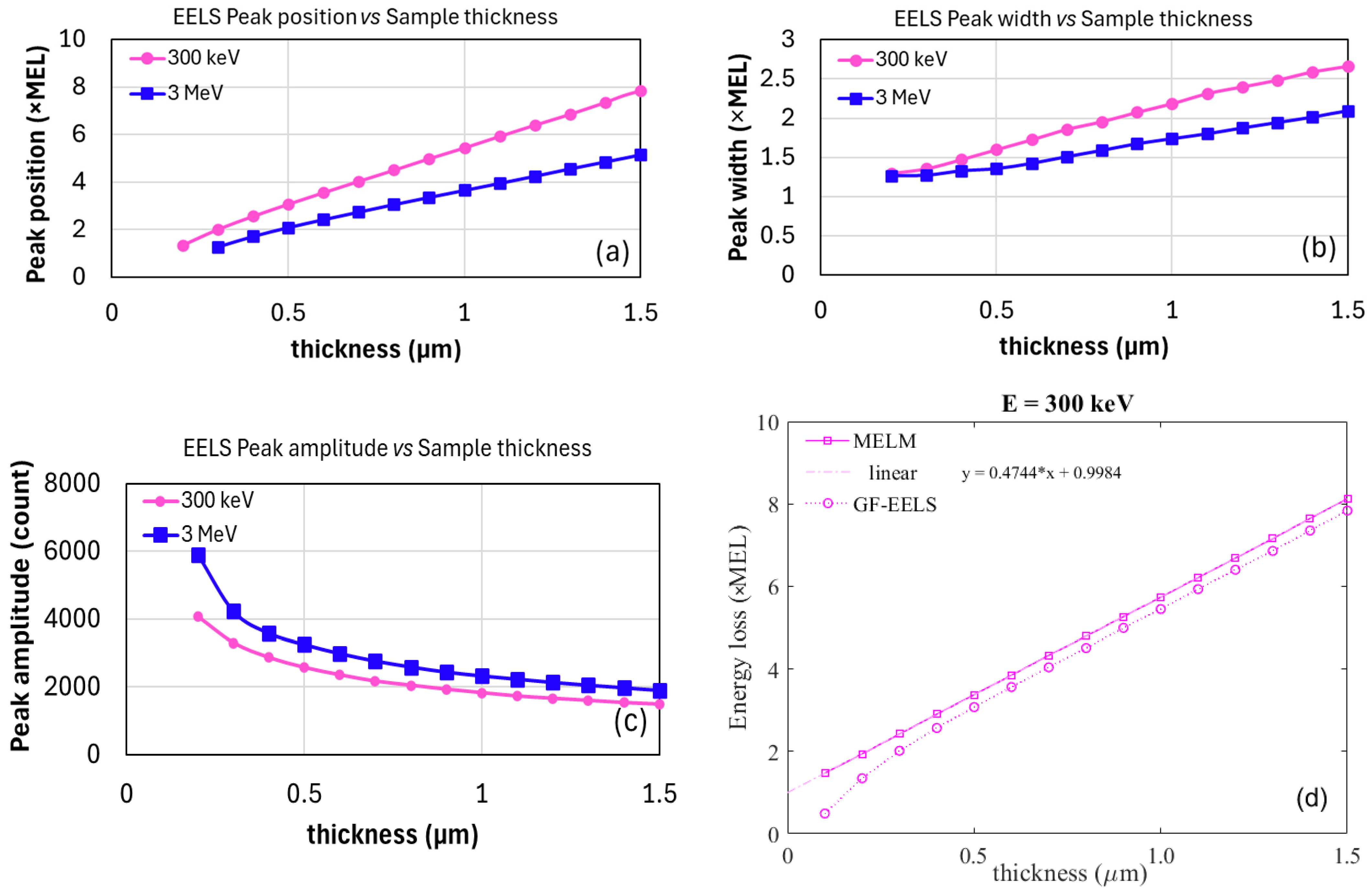
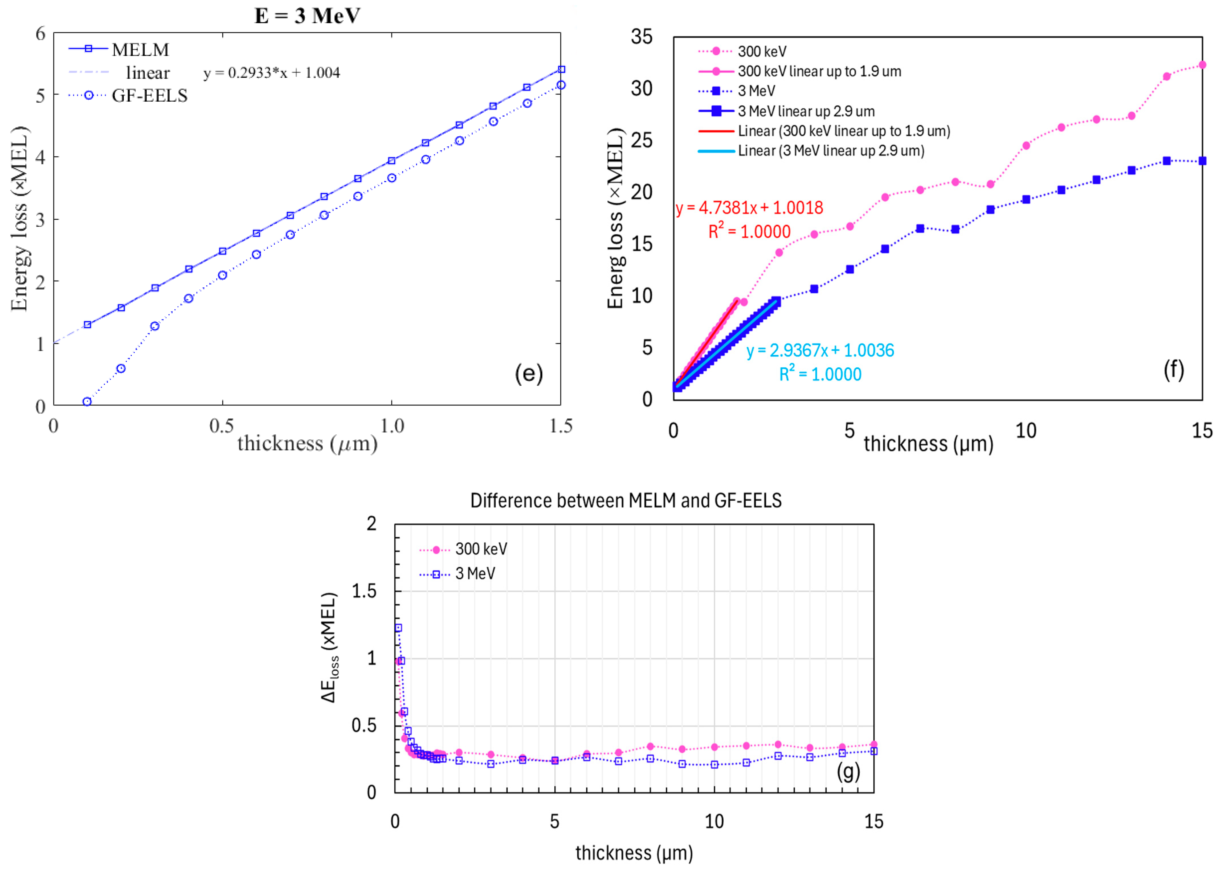
2.4. Simulating EELS for Thin Samples

MC simulations were conducted to obtain the EELS for 300 keV (Figure 3c) and 3 MeV (Figure 3d) beam energies for thin samples with thicknesses less than 2 μm. The corresponding peak positions, widths, and amplitudes were extracted using the GF-EELS method, as shown in Figure 5a–c, respectively.
In the thin-sample regime, the energy loss is nearly linearly proportional to the sample thickness. This linear relationship arises because the probability of inelastic scattering increases with thickness, leading to a corresponding increase in the average energy lost by the electrons as they pass through the sample.
Energy loss was analyzed using both MELM (solid lines) and GF-EELS (dashed lines) methods, as shown in Figure 5d–f. Significant discrepancies between the methods are observed when the sample thickness is ≤0.5 μm. However, these differences diminish as the thickness increases, stabilizing at a constant value of approximately 0.3 MEL units beyond 0.5 μm (Figure 5g). This behavior is expected, as the accuracy of Gaussian fitting decreases when the EELS peak approaches zero energy loss, making the results less reliable. The slight lower-energy shifts observed in the GF-EELS data are due to the tail contribution not fully captured by the Gaussian fit. This offset remains nearly constant (Figure 5g) and can be corrected. Once the electron energy is fixed, both methods predict the same slope, as shown in Figure 5d,e.
Additionally, to determine the maximum sample thickness where a linear relationship between energy loss and sample thickness is maintained, we performed linear fitting. The linear relationship holds up to 1.9 μm for 300 keV and 2.9 μm for 3 MeV, as shown in Figure 5f.

2.5. Differentiating Elastic and Inelastic Scattering via a Dipole Spectrometer

Energy-resolved angular broadening characterization is essential for distinguishing elastic from inelastic scattering processes, which involve scattering without and with energy loss, respectively. This distinction can be made by repeating the experiment with a zero-energy loss filter, consisting of a dipole spectrometer and a downstream aperture, as described in [21]. The scattering cross-section quantifies the probability of specific scattering events, emphasizing the need for experimental methods that can effectively differentiate elastic and inelastic scattering angle distributions. This is particularly important across a broad range of sample thicknesses, from a single to tens of MFPs, where both single and multiple elastic and inelastic events occur.
Accurate characterization of angular broadening and differentiation of elastic and inelastic contributions, as shown in Figure 6, as a function of sample thickness and composition, is critical yet challenging. In our previous studies, the detector signals we numerically simulated [6,21] were a mix of elastic and inelastic scattering events. The dipole spectrometer allows us to separate angular broadening caused by elastic and inelastic scattering.
The zero-energy loss filter can be operated in either ON or OFF mode. In the ON mode, only electrons with zero energy losses (including un-scattered, single elastically scattered, and multiple elastically scattered events) reach the detector, as illustrated in Figure 6a and Figure 6c for 300 keV and 3 MeV, respectively. In the OFF mode, similar to previous studies [6,22], both zero and non-zero energy loss electrons (including un-scattered, elastically scattered, and inelastically scattered events) are detected. Since angular broadening profiles for various sample thicknesses are similar to those in Figure 6a (300 KeV) and Figure 6c (3 MeV), we focus on the differences between the OFF and ON modes, as shown in Figure 6b,d. These differences represent the contribution from inelastic scattering only, improving measurement accuracy by isolating elastic scattering events.
Our previous study [6] demonstrated that the ratio of critical angles for elastic and inelastic scattering remains nearly constant across the electron energy range 0.3–3 MeV. Under zero-energy loss filter conditions, elastic scattering events typically produce much larger scattering angles compared to inelastic events. These measurements are crucial for accurately extrapolating the critical angles, refining scattering models, and enhancing our understanding of elastic and inelastic scattering processes in different materials.

3. Conclusions

In our previous study [6], we explored the interplay between sample thickness, electron energy, and resolution in high-energy electron microscopy, with a focus on MeV-STEM. This work extends those findings by providing valuable insights into estimating energy loss as a function of sample thickness and its impact on resolution, particularly in the context of TEM imaging mode. In comparing MeV-TEM with MeV-STEM, we emphasize that each mode offers distinct advantages for specific applications. MeV-TEM is particularly effective for studying local non-periodic structures, such as defects, vacancies, dislocations, and domains in condensed matter systems, providing sufficient spatial resolution for real-space imaging. However, its resolution is often limited by chromatic aberration, which is influenced by factors such as the objective lens’s chromatic aberration coefficient, electron energy spread, and convergence semi-angle. In TEM mode, energy spread induced by electron–sample interactions becomes a significant source degrading image qualities, especially for thicker samples. As sample thickness increases, energy loss accumulates, further degrading resolution.
To address this, we developed a simulation tool that estimates the EELS as a function of sample thickness across a broad range of electron beam energies (300 keV to 3 MeV). Leveraging advancements in MeV-TEM/STEM technology, we aim to refine electron beam parameters to minimize energy spread. By incorporating EELS capabilities into the BNL MC simulation code, we evaluate and optimize electron beam settings to mitigate the impact of electron–sample interactions on energy spread and resolution. For thin samples, inelastic scattering minimally affects energy loss, with resolution primarily determined by elastic scattering and aberrations. However, as sample thickness increases, inelastic scattering becomes more pronounced, exacerbating energy loss and further degrading resolution. This study advances our previous work by providing a systematic methodology to account for these effects and optimize beam parameters to enhance resolution in thicker samples.
Additionally, we developed a predictive model for mean energy loss as a function of sample thickness across a wide range of electron beam energies (300 keV to 3 MeV) [22]. EELS capabilities were integrated into the BNL-MC simulation code, and energy loss was computed using two methods: Gaussian fitting of the energy-loss peak and direct analysis of the energy loss distribution. Both thin (<2 μm) and thick (2–15 μm) samples were evaluated revealing that, while the methods yielded consistent results in most cases, significant discrepancies arose for very thin samples (<1 MFP), where Gaussian fitting introduced substantial errors due to the lack of a well-defined peak.
Key findings include the following: (a) Beam energy dependence: Energy loss is strongly influenced by electron beam energy, decreasing as the electron energy increases. (b) Thin samples (<2 μm): Energy loss exhibits a linear relationship with sample thickness across the entire energy range, including at 300 keV. (c) Thick samples (2 to 15 μm): The relationship between energy loss and sample thickness becomes nonlinear, especially for thicker samples, due to the increasing complexity from multiple scattering events. The linear relationship between energy loss and sample thickness holds up to 1.9 μm for an electron energy of 300 keV and up to 2.9 μm for 3 MeV (Figure 5f). These differences can be attributed to the fact that, at lower beam energies, elastic and inelastic critical angles are significantly larger (several milliradians or more, as observed in MeV-STEM studies [22] and listed in Table 2), increasing the likelihood of large-angle scattering. This results in longer effective electron path lengths and deviations from energy loss predictions based solely on sample thickness and MFP.
To experimentally validate these findings and precisely characterize MEL per inelastic scattering event, we propose utilizing the intensity profile in the dispersive direction of a standard magnetic spectrometer. By employing a wedged sample with varying, ranging from one to several tens of MFPs, we can systematically observe and analyze the effects. In future studies, we plan to use a silicon wafer as a model system to demonstrate the applicability of the wedge-shaped sample fabrication methodology to a wide range of materials. The analysis focuses on a silicon sample with a thickness range from 0.0 to 20.0 μm. The Metrology group at NSLS-II has a silicon wafer with dimensions of 30 mm × 10 mm × 20 μm, which can be used for this purpose. The wedged sample will be fabricated using the Focused Ion Beam with Shadow technique. Silicon, a commonly used substrate material in microchip production, serves as a representative material, while carbon, a low-Z material, is selected for its similarity to biological materials in terms of atomic composition. Furthermore, to fully leverage the EELS capabilities with the assistance of Artificial intelligence (AI) [23], it is essential to characterize angular broadening for both elastic and inelastic scattering in relation to sample thickness and composition, as shown in Figure 6. By incorporating AI, we can efficiently analyze and model these complex relationships, enabling more accurate predictions and a deeper understanding of scattering mechanisms. This comprehensive approach will form the foundation for our future investigations.

Author Contributions

Conceptualization, X.Y.; Methodology, X.Y.; Software, L.W.; Formal analysis, X.Y.; Investigation, V.S. and T.S.; Resources, V.S., T.S. and L.W.; Writing—original draft, X.Y.; Writing—review & editing, V.S., T.S. and L.W. All authors have read and agreed to the published version of the manuscript.

Funding

This work was supported by DOE under Contract No. DE-SC0012704 and partially supported by the BNL LDRD 22-029 and LBMS’ BER funding.

Data Availability Statement

The datasets generated and analyzed during the current study are not publicly available, due to the reason that we want to know who has an interest in our datasets, but are available from the corresponding author upon reasonable request.

Conflicts of Interest

The authors declare no competing financial and non-financial interests in relation to the work described in the paper.

Appendix A

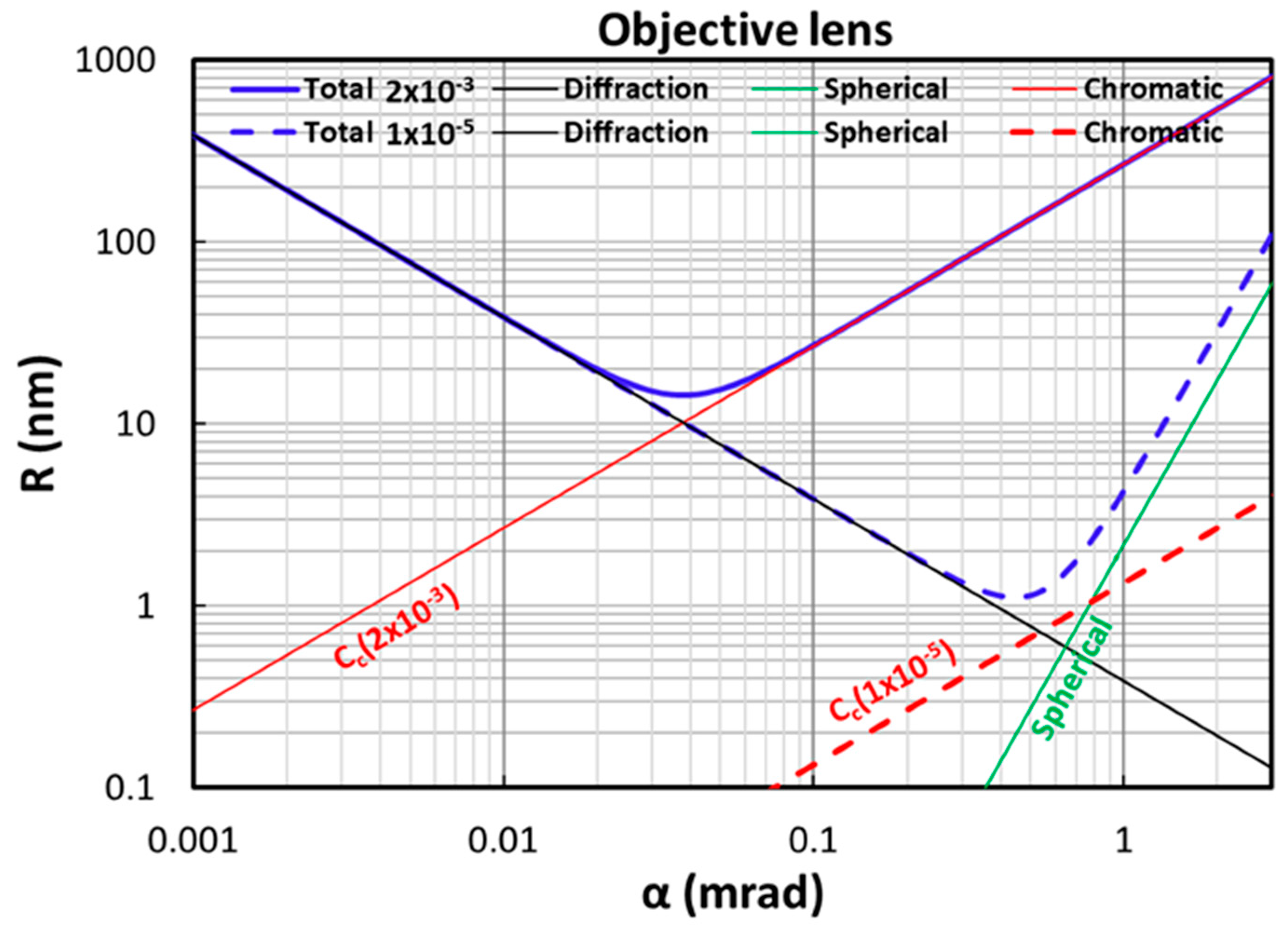
Appendix A.1. Beam Energy Spread Influence on TEM Resolution

Our previous study showed that achieving 1 nm resolution requires an energy spread of approximately 10−5 at a convergence semi-angle of α 0.5   m r a d . In contrast, an energy spread of 10−3 at the same α would degrade the resolution to over 10 nm, as shown in Figure A1 [8,9].
Figure A1. Resolution as a function of collection semi-angle, considering spherical aberration (green), chromatic aberration (red), and diffraction (black) contributions, for two energy spread conditions: 2 × 10⁻³ (solid blue) and 1 × 10⁻⁵ (dashed blue).
Electronics 14 00469 g0a1

Appendix A.2. Derivation of the Equivalence Between Two Methods: Gaussian Fitting and Direct Analysis

The EELS curve is assumed to follow a Gaussian distribution (Equation (A1))
1 2 π σ e E E p e a k 2 2 σ 2 d E ,
where σ and E p e a k are the standard deviation and the mean or expectation of the distribution, respectively. We replace the integral 0 I i n e l d Δ E in Equation (9) using a Gaussian distribution 1 2 π σ e E E p e a k 2 2 σ 2 d E . As a result, Equation (9) becomes Equation (A2).
1 2 π σ E · e E E p e a k 2 2 σ 2 d E 1 2 π σ e E E p e a k 2 2 σ 2 d E
Equation (A2) can be simplified as follows:
( E E p e a k ) · e E E p e a k 2 2 σ 2 d E + E p e a k · e E E p e a k 2 2 σ 2 d E e E E p e a k 2 2 σ 2 d E   = E p e a k · e ( E E p e a k ) 2 2 σ 2 d E e ( E E p e a k ) 2 2 σ 2 d E = E p e a k .
So far, we have mathematically derived that when the EELS curve follows a Gaussian distribution, the two methods, GF-EELS and MELM, are equivalent.

References

  1. Weiner, E.; Pinskey, J.M.; Nicastro, D.; Otegui, M.S. Electron microscopy for imaging organelles in plants and algae. Plant Physiol. 2022, 188, 713–725. [Google Scholar] [CrossRef] [PubMed]
  2. Böhning, J.; Bharat TA, M. Towards high-throughput in situ structural biology using electron cryotomography. Prog. Biophys. Mol. Biol. 2021, 160, 97–103. [Google Scholar] [CrossRef] [PubMed]
  3. Oikonomou, C.M.; Jensen, G.J. Cellular Electron Cryotomography: Toward Structural Biology In Situ. Annu. Rev. Biochem. 2017, 86, 873–896. [Google Scholar] [CrossRef]
  4. Otegui, M.S.; Pennington, J.G. Electron tomography in plant cell biology. Microscopy 2019, 68, 69–79. [Google Scholar] [CrossRef] [PubMed]
  5. Yang, X.; Wang, L.; Maxson, J.; Bartnik, A.C.; Kaemingk, M.; Wan, W.; Cultrera, L.; Wu, L.; Smaluk, V.; Shaftan, T.; et al. Towards Construction of a Novel Nanometer-resolution MeV-STEM for Imaging of Thick Frozen Biological Samples. Photonics 2024, 11, 252. [Google Scholar] [CrossRef]
  6. Yang, X.; Wang, L.; Smaluk, V.; Shaftan, T. Optimize electron beam energy toward in-situ imaging of large thick frozen bio-samples with nanometer resolution. Nanomaterials 2024, 14, 803. [Google Scholar] [CrossRef] [PubMed]
  7. Wang, L.; Yang, X. Monte Carlo Simulation of Electron Interactions in an MeV-STEM for Thick Frozen Biological Sample Imaging. Appl. Sci. 2024, 14, 1888. [Google Scholar] [CrossRef]
  8. Wan, W.; Chen, F.R.; Zhu, Y. Design of compact ultrafast microscopes for single- and multi-shot imaging with MeV electrons. Ultramicroscopy 2018, 194, 143–153. [Google Scholar] [CrossRef] [PubMed]
  9. Yang, X.; Smaluk, V.; Shaftan, T.; Wang, L.; McSweeney, S.; Yu, L.; Tiwari, G.; Hidaka, Y.; Wang, G.; Doom, L.; et al. Current Status of Developing Ultrafast Mega-Electron-Volt Electron Microscope; NSLSII-TN-ASD-383; Brookhaven National Laboratory (BNL): Upton, NY, USA, 2022. [Google Scholar]
  10. Wolf, S.G.; Shimoni, E.; Elbaum, M.; Houben, L. STEM Tomography in Biology. In Cellular Imaging: Electron Tomography and Related Technique; Hanssen, E., Ed.; Springer International Publishing: Cham, Switzerland, 2018; pp. 33–60. [Google Scholar]
  11. Reimer, L.; Kohl, H. Transmission Electron Microscopy, 5th ed.; Springer Science + Business Media, LLC.: New York, NY, USA, 2008. [Google Scholar]
  12. Henderson, R. The potential and limitations of neutrons, electrons and X-rays for atomic resolution microscopy of unstained biological molecules. Q. Rev. Biophys. 1995, 28, 171–193. [Google Scholar] [CrossRef] [PubMed]
  13. Peet, M.J.; Henderson, R.; Russo, C.J. The energy dependence of contrast and damage in electron cryomicroscopy of biological molecules. Ultramicroscopy 2019, 203, 125–131. [Google Scholar] [CrossRef]
  14. Langmore, J.P.; Smith, M.F. Quantitative energy-filtered electron-microscopy of biological molecules in ice. Ultramicroscopy 1992, 46, 349–373. [Google Scholar] [CrossRef] [PubMed]
  15. Jacobsen, C.; Medenwaldt, R.; Williams, S. X-Ray Microscopy and Spectromicroscopy: Status Report from the Fifth International Conference, Würzburg, August 19–23, 1996; Thieme, J., Schmahl, G., Rudolph, D., Umbach, E., Eds.; Springer: Berlin/Heidelberg, Germany, 1998; pp. 197–206. [Google Scholar]
  16. Du, M.; Jacobsen, C. Relative merits and limiting factors for X-ray and electron microscopy of thick, hydrated organic materials. Ultramicroscopy 2018, 184, 293–309. [Google Scholar] [CrossRef] [PubMed]
  17. Egerton, R.F. Choice of operating voltage for a transmission electron microscope. Ultramicroscopy 2014, 145, 85–93. [Google Scholar] [CrossRef]
  18. Tanaka, N. Electron Nano-Imaging, 1st ed.; Springer: Tokyo, Japan, 2017. [Google Scholar]
  19. Pante, I.; Cucinotta, F.A. Cross sections for the interactions of 1 eV–100 MeV electrons in liquid water and application to Monte-Carlo simulation of HZE radiation tracks. New J. Phys. 2009, 11, 063047. [Google Scholar] [CrossRef]
  20. Quintard, B.; Yang, X.; Wang, L. Quantitative Modeling of High-Energy Electron Scattering in Thick Samples Using Monte Carlo Techniques. Appl. Sci. 2025, 15, 565. [Google Scholar] [CrossRef]
  21. Photoelectron Generated Amplified Spontaneous Radiation Source (PEGASUS). Available online: http://pbpl.physics.ucla.edu/pages/pegasus.html (accessed on 20 October 2024).
  22. Yang, X.; Wang, L.; Smaluk, V.; Shaftan, T.; Wang, T.; Bouet, N.; D’Amen, G.; Wan, W.; Musumeci, P. Simulation Study of High-Precision Characterization of MeV Electron Interactions for Advanced Nano-Imaging of Thick Biological Samples and Microchips. Nanomaterials 2024, 14, 1797. [Google Scholar] [CrossRef] [PubMed]
  23. Xu, S.; Manshaii, F.; Xiao, X.; Chen, J. Artificial intelligence assisted nanogenerator applications. J. Mater. Chem. A 2025, 13, 832. [Google Scholar] [CrossRef]
Figure 1. The normalized energy loss of the amorphous ice sample as a function of sample thickness was calculated using the mean-energy-loss method (described in Section 2.3.2), for two different electron beam energies: 300 keV (magenta) and 3 MeV (blue).
Electronics 14 00469 g001
Figure 2. The estimated MFP as a function of electron energy for an amorphous ice sample, based on our early study [5,6], is shown.
Electronics 14 00469 g002
Figure 3. Histograms of energy loss in units of MEL per inelastic scattering event for sample thicknesses up to 15 μm, including 1 μm (red), 3 μm (magenta), 5 μm (blue), 10 μm (green) and 15 μm (cyan), at electron beam energies of 300 keV with M E L = 39.9   e V (a) and 3 MeV with M E L = 102.8   e V (b). In the thin sample regime, histograms for different sample thicknesses, 0.1 μm (red), 0.3 μm (magenta), 0.5 μm (blue), 1.0 μm (green) and 1.5 μm (cyan), are shown for 300 keV (c) and 3 MeV (d), respectively.
Electronics 14 00469 g003
Figure 4. (a) Gaussian fitting of the EELS curve for a 1 μm thick sample at 300 keV is used as an example to extract the peak position, width, and amplitude, a method referred to as GF-EELS. GF-EELS analysis was applied to the MC simulation results for thick samples up to 15 μm, with electron beam energies of 300 keV (magenta) and 3 MeV (blue), extracting the peak positions (b), peak widths (c), and peak amplitudes (d). Energy loss was analyzed using two methods: GF-EELS (dashed lines) and MELM (solid lines). The energy loss as a function of sample thickness is shown for two electron beam energies: (e) 300 keV and (f) 3 MeV. Panel (g) displays the energy loss estimated using MELM for 300 keV (magenta) and 3 MeV (blue). The vertical axis represents the energy loss in units of MEL per inelastic scattering event, which varies with electron beam energy.
Electronics 14 00469 g004aElectronics 14 00469 g004b
Figure 5. In the thin sample range of 0 to1.5 μm, we apply GF-EELS to analyze MC simulation results for two different electron beam energies: 300 keV (magenta) and 3 MeV (blue). This analysis provides the peak positions (a), peak widths (b), and peak amplitudes (c). Additionally, energy loss is analyzed using two methods: GF-EELS (dashed lines) and MELM (solid lines). The energy loss as a function of sample thickness is shown for two electron beam energies: (d) 300 keV and (e) 3 MeV. Panel (f) shows the energy loss estimated via MELM for 300 keV (magenta) and 3 MeV (blue). The vertical axis represents the energy loss in units of MEL per inelastic scattering event. A linear relationship between energy loss and sample thickness is maintained for the 300 keV case up to a thickness of 1.9 μm and for the 3 MeV case up to 2.9 μm. (g) The difference in energy loss obtained using MELM and GF-EELS is plotted for 300 keV (magenta) and 3 MeV (blue) as the sample thickness increases from 0.1 to 15 μm.
Electronics 14 00469 g005aElectronics 14 00469 g005b
Figure 6. For an electron beam energy of 300 KeV, panels (a,b) display the cumulative angle profiles for elastic and inelastic scattering, respectively, for various sample thicknesses: 1 μm (red), 5 μm (blue), 10 μm (green) and 15 μm (cyan). The bin width was 1 mrad for elastic scattering and 0.1 mrad for inelastic scattering. For an electron beam energy of 3 MeV, panels (c,d) show the corresponding cumulative angle profiles for elastic and inelastic scattering at the same sample thickness. The bin width was 0.1 mrad for elastic scattering and 0.05 mrad for inelastic scattering. The high noise level observed in panels (a,c) is primarily due to the small bin widths. These bin widths were selected to retain more detail in the plots.
Electronics 14 00469 g006
Table 1. Electron beam parameters used as input for MC simulations.
EdsamαE/Eϵgeo
MeVnmmrad pm·rad
3.021<10−42
Table 2. Electron scattering cross-section for oxygen from 300 keV to 3 MeV. θ0 and θE are the characteristic scattering angles for elastic and inelastic scattering.
Elastic Cross-Section (nm2) Inelastic Cross-Section (nm2)
Detector Collection Angle Detector Collection Angle
Electron energy (eV)θ0 (mrad)0–10 mrad10–50 mrad50–100 mradTotalθE (mrad)0–10 mrad10–50 mrad50–100 mradTotal
300,00011.82.1 × 10−52.6 × 10−52.6 × 10−65.0 × 10−50.0809.4 × 10−56.8 × 10−63.4 × 10−71.0 × 10⁻⁴
3,000,0002.12.9 × 10−51.3 × 10−65.5 × 10−83.1 × 10−50.0114.1 × 10−51.7 × 10−76.9 × 10−94.1 × 10⁻⁵
Disclaimer/Publisher’s Note: The statements, opinions and data contained in all publications are solely those of the individual author(s) and contributor(s) and not of MDPI and/or the editor(s). MDPI and/or the editor(s) disclaim responsibility for any injury to people or property resulting from any ideas, methods, instructions or products referred to in the content.

