Article

A Memory-Efficient Compensation Algorithm for Vertical Crosstalk in 8K LCD Panels

by
Yongwoo Lee
1,2,
Kiwon Choi
1,
Hyeryoung Park
2,
Yong Ju Kim
1,
Kookhyun Choi
2,*,
Jae-Hong Jeon
3,* and
Min Jae Ko
1,4,*
1
Department of Chemical Engineering, Hanyang University, Seoul 04763, Republic of Korea
2
Samsung Display Co., Ltd., Yongin 17113, Republic of Korea
3
School of Electronics and Information Engineering, Korea Aerospace University, Goyang 10540, Republic of Korea
4
Department of Battery Engineering, Hanyang University, Seoul 04763, Republic of Korea
*
Authors to whom correspondence should be addressed.
Electronics 2025, 14(19), 3965; https://doi.org/10.3390/electronics14193965
Submission received: 30 August 2025 / Revised: 7 October 2025 / Accepted: 8 October 2025 / Published: 9 October 2025
(This article belongs to the Section Electronic Materials, Devices and Applications)

Abstract

As ultra-high resolution liquid crystal displays (LCDs) advance, crosstalk has become a critical challenge due to the reduced spacing of electronic circuits and increased signal frequencies. In particular, vertical crosstalk (V-CT) in vertical-alignment LCDs arises mainly from fringing electric fields generated by data lines, along with secondary contributions from data line–pixel coupling effect, thin-film transistor leakage, and other factors. To resolve V-CT, we propose a memory-efficient compensation algorithm implemented on a field-programmable gate array as a customized timing controller. The proposed algorithm achieves compensation accuracy within 2% while significantly reducing memory requirements. A conventional 7680 × 4320 pixel LCD panel requires approximately 796 MB of memory for compensation data, whereas our method reduces this to only 0.37 MB—a nearly 2000-fold reduction—by referencing only preceding pixel information. This approach enables cost-effective implementation, faster processing, and enhanced image quality. Overall, the proposed method provides a practical and scalable solution for resolving V-CT in 8K LCD panels, establishing a new benchmark for high-resolution display technologies.

1. Introduction

In recent years, display technology has rapidly advanced from standard definition to high definition and, more recently, to ultra-high definition. However, the transition to higher resolutions has introduced substantial technical challenges [1,2,3,4]. In particular, increasing the pixel density within fixed panel dimensions requires a greater number of signal lines and a narrower spacing between adjacent elements that constitute a pixel. Under such conditions, ultra-high-resolution liquid crystal displays (LCDs), such as 8K, are highly susceptible to crosstalk—undesired interference between adjacent elements. Among these, vertical crosstalk (V-CT), which results from interactions between pixels and vertical signal lines (i.e., data lines), poses a critical threat to image quality in ultra-high-resolution LCDs.
A detailed understanding of LCD operation is essential for addressing this issue. As shown in Figure 1, each pixel contains a thin-film transistor (TFT) that acts as a switch, transferring the data voltage from the data line to the pixel [5,6]. The transferred data voltage determines the luminance of the pixel. Additionally, a pixel storage capacitor (Cst) plays a vital role in maintaining the transferred data voltage between refresh cycles. The two electrodes of the storage capacitor are the pixel and common -voltage (Vcom) electrodes. As display resolution increases, for example, in 8K panels operating at 120 Hz, the design of data and gate lines becomes increasingly complex, thereby amplifying the likelihood of signal interference.
V-CT has become a particularly critical issue in 8K LCDs due to the partial overlap between the data line and the pixel electrode in practical panel designs, along with the narrow spacing between them [7]. Under these conditions, strong fringing electric fields are generated around the data lines, which significantly disturb the tilt angle of the liquid crystal (LC) molecules and result in visible image artifacts. Prior efforts to resolve V-CT have primarily focused on two strategies: (i) design-based approaches, such as shielding structures to reduce interference [8,9], and (ii) compensation algorithms that correct signal distortions [10]. The latter strategy is considered more practical from an industrial engineering perspective because it does not require major design modifications and significant financial resources. However, although this approach has achieved limited success, it also demands large memory resources in the driving circuits, thereby imposing relatively high implementation costs.
In this study, we present a novel compensation algorithm that effectively suppresses V-CT in 8K vertical-alignment (VA) LCDs while significantly reducing memory requirements. Unlike conventional methods that rely on storing large volumes of compensation data, our approach requires only minimal data extracted from an adjacent pixel in the preceding and current frames. Our memory-efficient algorithm enables faster processing, cost-effective implementation, and improved image quality, thereby providing a practical solution for next-generation high-resolution displays.

2. Mechanism of Vertical Crosstalk in LCD

Crosstalk refers to visual defects in LCDs that arise from the interference between adjacent elements. For instance, when the voltage stored in the storage capacitor is influenced by voltage swings on the signal lines, the brightness and color of pixels can be distorted, leading to noticeable image artifacts. Such artifacts often appear as abnormal rectangular patterns in either the horizontal or vertical direction in matrix-type displays. Among the various types, V-CT is particularly problematic in 8K LCDs, as the dense pixel layout and high operating frequencies intensify interference effects [11]. The primary causes of V-CT can be summarized as follows:
  • Data line–pixel coupling: The capacitance asymmetry between the data line and pixel electrode (Cdp) can induce undesired variations in the voltages stored in the pixel storage capacitors and the resulting brightness fluctuations.
  • Fringing electric fields generated by the data line: Partial overlap between the data line and the pixel electrode produces undesired strong local electric fields that alter the tilt angle of LC molecules, leading to noticeable brightness variations [12,13]. This effect has been identified as the dominant factor in high-resolution LCDs.
  • TFT leakage current: Imperfections in TFTs may cause charge loss in pixel storage capacitors. However, under standard operating conditions, this effect is generally less significant and becomes particularly minor at high frequencies.
Figure 2 and Table 1 summarize the primary causes of V-CT in 8K LCDs. Each of these factors contributes to pixel luminance instability, resulting in V-CT. Although the data line–pixel coupling has generally been regarded as the cause of V-CT, the fringing electric fields from the data line have become the dominant factor in high-resolution LCDs. Therefore, our compensation algorithm was developed with a focus on reducing V-CT caused by the fringing electric fields from the data line.

3. Proposed Compensation Method for V-CT

In general, data compensation for resolving V-CT relies on the timing controller (T-con), which generates the data signals delivered to each pixel array. In this method, stored pixel voltage data are used to generate new compensated voltages based on image patterns and background luminance. Although effective, this approach requires a large memory capacity, especially for ultra-high-resolution panels, as shown in Figure 3. Figure 3 shows that the number of pixels in a 4K resolution panel is four times greater than that of an FHD panel, and an 8K panel contains four times more pixels than a 4K panel. This multiplication factor also represents the rate at which the data volume required for the T-con increases when conventional data compensation methods are employed to resolve V-CT. To resolve this issue, we designed a more efficient algorithm that reduces memory requirements without compromising the accuracy of compensation.
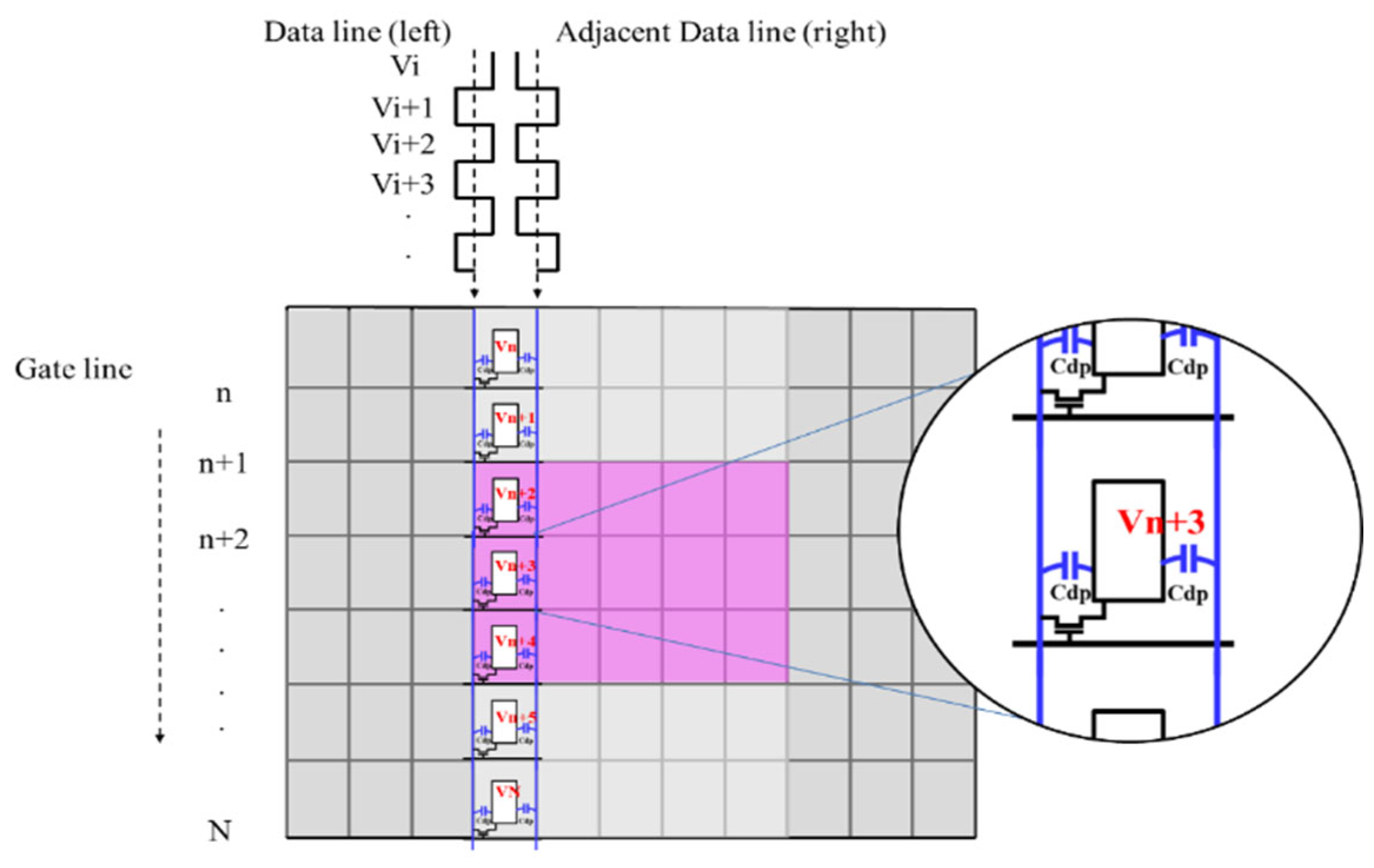
Because a data line delivers voltages to all pixels in the same column, the stored voltage of an individual pixel generally differs from the instantaneous voltage of the data line. This voltage discrepancy generates fringing fields that cause the LC molecules at the pixel edges to tilt differently from those in the interior. Figure 4 illustrates this interaction, highlighting how the signal voltages of the data lines interact with the pixel. Consequently, the average luminance of the pixel deviates from its intended value, resulting in visible V-CT.
Equations (1)–(3) describe how luminance distortion in a pixel is converted into an equivalent voltage caused by fringing fields from adjacent data lines. Equation (1) represents the effect of the left data line as an equivalent distortion voltage (ΔVn_left), and Equation (2) represents the effect of the right data line (ΔVn_right). Equation (3) combines both contributions to yield the total distortion ΔVn. Here, Vn is the voltage stored in the pixel on the nth line. The nth line is one of the total N lines, where N represents the number of pixels arranged in the vertical direction. Vi_left and Vi_right denote the signal voltages of the adjacent data lines in the current frame, while V*i_left and V*i_right denote those in the previous frame; δ is an experimentally determined proportionality constant that relates the voltage difference to luminance distortion.
V n _ l e f t = δ × i = n + 1 N V i _ l e f t * V n + i = 1 n V i _ l e f t V n × 1 N
V n _ r i g h t = δ × i = n + 1 N V i _ r i g h t * V n + i = 1 n V i _ r i g h t V n × 1 N
V n = V n _ l e f t + V n _ r i g h t
In practice, calculating ΔVn requires recalling N signal voltages for each column (e.g., N = 4320 for an 8K panel), which imposes a substantial memory burden.
To alleviate this demand, we introduce the following cumulative summation terms. Equation (4) defines Sn_left as the cumulative summation of the voltage differences between the left data line signals and the nth pixel voltage, whereas Equation (5) defines S(n−1)_left for the (n − 1)th pixel.
S n _ l e f t = i = n + 1 N V i _ l e f t * V n + i = 1 n ( V i _ l e f t V n ) = V n + 1 * V n + V n + 2 * V n + + V N * V n + V i V n + V 2 V n + + V n V n
S ( n 1 ) _ l e f t = i = n N V i _ l e f t * V n 1 + i = 1 n 1 ( V i _ l e f t V n 1 ) = V n * V n 1 + V n + 1 * V n 1 + + V N * V n 1 + V 1 V n + 1 + V 2 V n 1 + + V n 1 V n 1
Subtracting Equation (5) from Equation (4) yields Equation (6). Importantly, by applying the reasonable assumption that the pixel voltages in the current frame do not differ significantly from those in the previous frame (Vn     Vn−1), the recurrence relation can be significantly simplified.
S n _ l e f t S ( n 1 ) _ l e f t + N × V n 1 V n
An identical process applies to Sn_right and S(n−1)_right for the right data line. Thus, each cumulative summation term requires only three values—its previous state, Vn−1, and Vn—rather than all N signal voltages. This recurrence formulation means that the algorithm requires only the last step instead of the entire history, drastically reducing memory demand.
Finally, ΔVn is obtained by combining the left and right contributions, as expressed in Equation (7).
V n = V n _ l e f t + V n _ r i g h t = δ × S n _ l e f t + S n _ r i g h t × 1 N  

4. Experimental Results and Discussion

4.1. Implementation Methods

In LCD panels, the T-con processes gray-level data to generate the displayed image. Because the V-CT compensation IP core is integrated into the T-con, our approach focuses on adjusting gray-levels rather than directly modifying pixel voltages. The compensation process using our algorithm can be summarized as follows. When a box pattern is displayed at the center of the LCD screen, luminance distortion appears above and below the box in the uncompensated state; this luminance deviation is denoted as ΔTn. As described in the previous section, we converted ΔTn into ΔVn, the equivalent voltage, which can be obtained using Equation (7). Finally, to suppress the perception of V-CT by the observer, a new voltage (Vn   =   Vn     ΔVn) should be applied to the pixels located above and below the box pattern, instead of the original voltage (Vn). Since the T-con is the component responsible for generating gray-levels, the corresponding gray-level for this new voltage (Vn′) should be determined as the T-con output. V-CT compensation is realized using the T-con through this process.
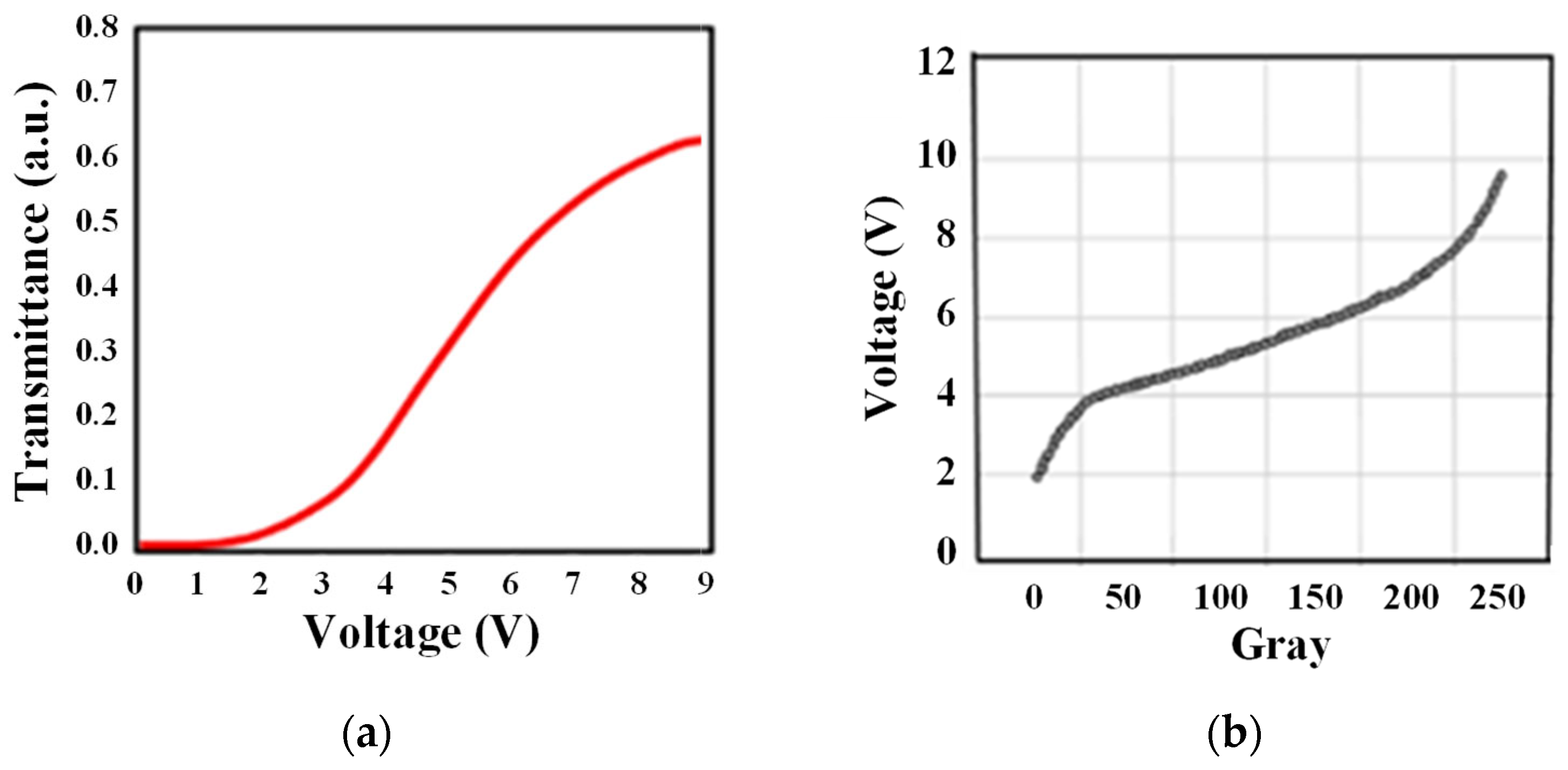
Although the above description outlines the compensation process in a simplified manner, its practical implementation is complicated by two key factors: the nonlinear voltage–transmittance (V–T) characteristics and the nonlinear voltage–gray-level (V–G) relationship. Figure 5 shows the V–T characteristics and the V–G relationship of a VA LCD panel.
The first complication arising from the nonlinear V–T characteristics is that, even with the same ΔV, its impact on ΔT varies depending on the pixel voltage (Vn). As a result, the proportionality constant δ required to compute ΔVn in Equation (7) varies depending on the pixel voltage (Vn). Although it is extremely difficult to derive δ as a closed-form function of Vn, it is possible to approximate δ values for each of the 256 gray-levels through carefully designed experiments. In our study, we quantified the level of V-CT under various conditions—such as the size of the box pattern, the gray-level of the box, and the gray-level of the background—and from these measurements, we derived approximate δ values for all 256 levels of Vn. Figure 6 shows the quantified V-CT values obtained from the above experiments, which were used to determine the δ values. In Figure 6a, the box size was fixed at 50% of the screen height, while the box and the background gray-levels were varied to measure the resulting V-CT. In Figure 6b, the box gray-level was fixed at 250 G, and the box size and the background gray-level were varied for the measurements. The V-CT value, which represents the degree of crosstalk, was obtained using Equation (8).
V e r t i c a l   c r o s s t a l k   % = L 1 L 2 / L 1 × 100
L 1 : L u m i n a c e   i n   c r o s s t a l k   r e g i o n , L 2 : L u m i n a n c e   i n   n o r m a l   r e g i o n
The second factor complicating the implementation—beyond the description presented at the beginning of this subsection—arises from the nonlinearity of the V–G relationship shown in Figure 5b. This nonlinearity arises from two factors: the application of gamma correction to compensate for the sensitivity of the human visual system to to luminance [14,15] and the inherent nonlinearity of the V–T characteristics of the LC, which promote the nonlinearity. As a result, even when a new voltage (Vn   =   Vn     ΔVn) is obtained from the calculation, it is not straightforward to identify a corresponding gray-level that precisely matches Vn′. Furthermore, performing such operations for every pixel in the T-con would impose a significant processing burden.
Therefore, once ΔVn is calculated, it is necessary to determine ΔGn, which indicates how many gray-level steps should be adjusted from the original gray-level (Gn). To facilitate implementation, we approximated the relationship between ΔGn and ΔVn as linear and introduced a compensation coefficient f(Gn) for each gray-level. Equation (9) defines the linear relationship between ΔGn and ΔVn, where f(Gn) serves as the proportional constant. Figure 7 shows the optimal f(Gn) values derived from both the V–T curve and the V–G relationship. Consequently, for V-CT compensation, the gray-level applied to each pixel is adjusted from the original Gn to Gn   =   Gn     ΔGn. Since ΔGn obtained from Equation (9) is generally non-integer, Gn′ also becomes non-integer. In such cases, the T-con must be programmed to select the nearest gray-level to Gn′.
G n = f ( G n ) × V n
For hardware verification, the proposed algorithm was implemented on an FPGA-based evaluation board (Xilinx, San Jose, CA, USA). The computation blocks were described using the VHSIC hardware description language (VHDL). Figure 8 shows the block diagram of the proposed V-CT compensation method. Module 3 first converts the input gray-levels into the voltage domain. Module 1 then aggregates the data for one frame. Module 2 then determines the compensated gray-level for each pixel using a lookup table containing the necessary tuning parameters.
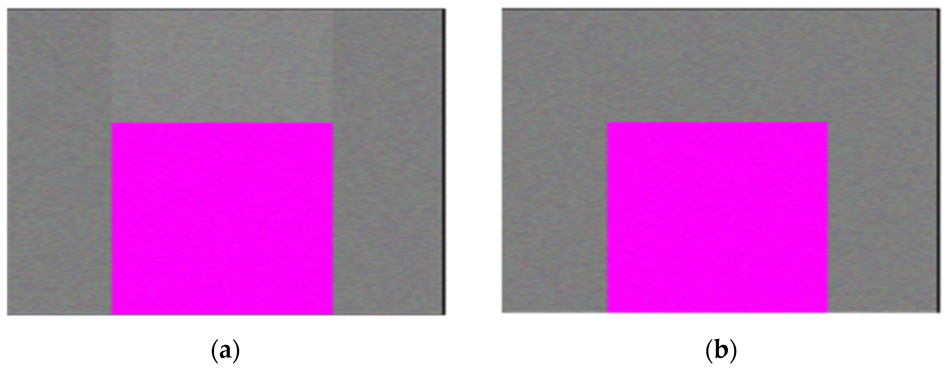
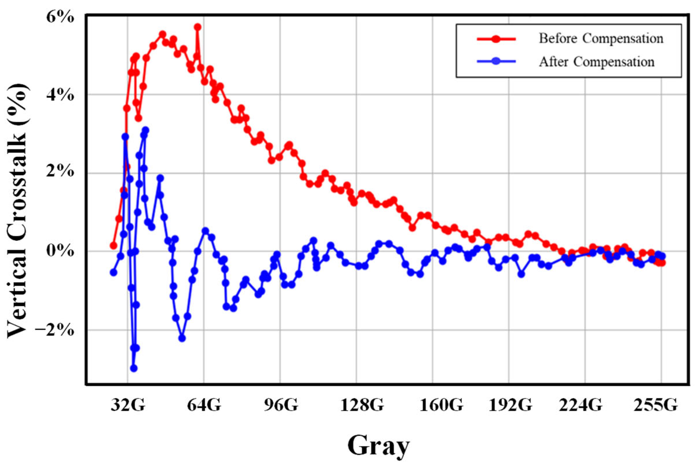
To evaluate the proposed compensation method, an 8K 120 Hz panel was employed. This configuration enhances the fringing-field effect, particularly when a colored window is displayed. We selected the 8K 120 Hz panel in this study because this configuration is widely adopted as a standard in high-end LCD evaluations, balancing practical availability with strict performance requirements. While higher refresh rates, such as 144 Hz, are also of interest, these were reserved for future investigation. Figure 9 shows the image compensated after applying the proposed method. Figure 10 presents the V-CT values as a function of the background gray-level, comparing the results before and after V-CT compensation. The results indicate that the proposed method considerably reduces the V-CT with appropriately tuned parameters.

4.2. Comparison of the Memory Requirements

An 8K panel with a resolution of 7680 × 4320 contains 99,532,800 RGB subpixels. Conventional compensation methods require approximately 796 MB of memory to store precomputed voltage values for each subpixel. In contrast, our algorithm requires only 0.37 MB, representing an approximately 2000-fold reduction.
This efficiency results from Equation (7), which references only the preceding pixel when calculating the compensation voltage, thereby minimizing the computational overhead. These results confirm that the proposed algorithm enables the practical implementation of V-CT compensation in 8K LCDs, providing both high efficiency and substantial hardware cost savings.

4.3. Comparison with the Existing Compensation Methods

Recent research efforts have approached the suppression of crosstalk and mura artifacts in LCD panels from different perspectives. To position our study within prior research, we compare it with representative approaches commonly used to suppress display artifacts. We consider the conventional pre-storage compensation method widely used in practice (no specific citation) as a baseline, which relies on full-panel pre-stored correction maps. Although effective in many cases, these methods scale poorly with resolution and typically require substantial memory capacity and periodic recalibration. Zhang et al. [10] proposed an efficient camera-based mura compensation system that leverages hardware–software co-optimization to correct luminance deviations, demonstrating strong performance with reduced hardware overhead, but still demanding significant storage and computation for ultra-high-resolution panels. Smorfa et al. [16] presented a physical-level driver model and simulator for analyzing pixel crosstalk phenomena. Their work provided an essential tool for evaluating new driver schemes and understanding the physical interactions among TFT leakage, line capacitance, and pixel storage capacitors. Although this simulator is powerful for design exploration, it does not directly propose a hardware-implementable compensation algorithm; therefore, it does not resolve the memory bottleneck encountered in T-cons for high-resolution panels. Historically, Yamada et al. [17] introduced a driving method for TFT-LCDs to improve pixel charging and reduce crosstalk under limited line times. This study represents the early development of compensation strategies at level of circuit driving. However, it predates the advent of ultra-high-resolution panels and thus does not address the scalability and memory requirements that dominate modern T-con design. In contrast, our study introduces a memory-efficient recurrence-based algorithm that directly targets vertical crosstalk while minimizing both computational and memory burdens, as summarized in Table 2.

4.4. Performance Considerations and Limitations

Several potential drawbacks commonly associated with optimization algorithms in high-resolution LCDs were examined. First, regarding image quality, our experimental results indicate that the proposed compensation improves visual clarity rather than degrading it. Second, in terms of algorithm complexity, the recurrence formulation requires only the previous state for each pixel, which simplifies both computation and memory usage compared with conventional LUT-based methods. Third, with respect to compatibility, the scheme is implemented at the T-con level and was successfully realized on an FPGA T-con without requiring any hardware modifications, demonstrating its practicality. Finally, concerning color accuracy, box-pattern experiments show that the method does not introduce noticeable chromatic distortion.
Beyond memory efficiency and compensation accuracy, broader performance aspects of high-resolution LCD driving schemes must also be considered. The introduction of compensation algorithms may affect factors such as power consumption, response time, signal accuracy, and the dynamic storage characteristics of TFTs. Although the present study focused on resolving vertical crosstalk caused by the fringing fields from the data line, quantitative evaluations of these additional aspects were not within the scope of this study and remain subjects for future investigation.
The robustness of the algorithm under diverse operating conditions also remains an important area for future work. Future studies should evaluate its performance across different refresh rates (e.g., 144 Hz), panel sizes, and environmental temperatures to confirm consistency and scalability. Such investigations are essential for establishing the general applicability of the proposed method in practical settings.
In addition, recent advances in 2D memory devices demonstrate the potential of atomically thin materials for ultra-fast, low-power memory applications [18]. For example, SnSe2/h-BN/graphene heterostructure devices have achieved ON/OFF ratios of ~106, nanosecond-scale program/erase speeds, and multi-bit storage capability. Such material-level innovations represent a complementary route to improving signal integrity and energy efficiency in next-generation electronic systems and may be combined with algorithmic solutions, such as those proposed in the present work.

5. Conclusions

In this study, we developed a memory-efficient compensation algorithm to resolve V-CT in high-resolution LCD panels. The proposed method was implemented on an FPGA as a T-con and achieved compensation accuracy within a 2% error margin while drastically reducing memory requirements. Specifically, for an 8K LCD panel (7680 × 4320), the required memory was reduced from approximately 796 MB to only 0.37 MB—approximately 1/2000 of conventional approaches.
The algorithm minimizes computational complexity by referencing only the preceding pixel data during compensation, enabling both faster processing and lower hardware costs. The experimental results demonstrated that the method effectively suppressed V-CT dominated by fringing fields, thereby improving image clarity and overall display quality.
The proposed approach provides a scalable and practical solution for next-generation 8K LCDs, establishing a new benchmark for efficient crosstalk compensation. Beyond V-CT suppression, the framework can be extended to address other forms of signal distortion, thereby contributing to the advancement of high-performance display technologies.

Author Contributions

Conceptualization, Y.L., K.C. (Kookhyun Choi), J.-H.J. and M.J.K.; coding and data curation, Y. L., K.C. (Kiwon Choi), H.P. and Y.J.K.; writing—original draft, review, and editing, Y.L., K.C. (Kookhyun Choi), J.-H.J. and M.J.K. All authors have read and agreed to the published version of the manuscript.

Funding

This work was supported in part by the GRRC program of Gyeonggi Province (GRRC-KAU-2025-B01, Development of Cinema Sound-Transmissive Display for the Substitution for Traditional Projector and Screen Systems) and by the Korea Institute of Energy Technology Evaluation and Planning (KETEP) grant funded by the Korea government (MOTIE) (Sector coupling energy industry advancement manpower training program, RS-2022-KP002703).

Data Availability Statement

The original contributions presented in this study are included in the article. Further inquiries can be directed to the corresponding authors.

Conflicts of Interest

The authors Hyeryoung Park and Kookhyun Choi were employed by the company Samsung Display Co., Ltd. The remaining authors declare that the research was conducted in the absence of any commercial or financial relationships that could be construed as a potential conflict of interest.

References

  1. Bae, K.S.; Oh, M.; Park, B.; Cho, Y.J.; Cho, S.H.; Kim, D. 51-1: Novel pixel structure for 8K QUHD LCD panel with enhanced optical performance. In Proceedings of the SID Symposium Digest of Technical Papers, San Jose, CA, USA, 14–15 May 2019; Wiley: Hoboken, NJ, USA, 2019; Volume 50, pp. 703–706. [Google Scholar] [CrossRef]
  2. Tan, G.; Huang, Y.; Li, M.-C.; Lee, S.-L.; Wu, S.-T. High dynamic range liquid crystal displays with a mini-LED backlight. Opt. Express 2018, 26, 16572–16584. [Google Scholar] [CrossRef] [PubMed]
  3. Alt, P.M.; Pleshko, P. Scanning limitations of liquid-crystal displays. IEEE Trans. Electron Devices 1974, 21, 146–155. [Google Scholar] [CrossRef]
  4. Hara, Y.; Kikuchi, T.; Kitagawa, H. IGZO-TFT technology for large-screen 8K display. J. Soc. Inf. Disp. 2018, 26, 169–177. [Google Scholar] [CrossRef]
  5. den Boer, W. Active Matrix Liquid Crystal Displays: Fundamentals and Applications, 1st ed.; Elsevier: Oxford, UK, 2005; ISBN 978-0-7506-7813-1. [Google Scholar]
  6. Chen, R.H. Liquid Crystal Displays: Fundamental Physics and Technology; Wiley: Hoboken, NJ, USA, 2011; ISBN 978-0470930878. [Google Scholar]
  7. Badano, A.; Kanicki, J. Characterization of crosstalk in high-resolution active-matrix liquid crystal displays for medical imaging. In Flat Panel Display Technology and Display Metrology II, Proceedings of the Photonics West 2001-Electronic Imaging, San Jose, CA, USA, 30 April 2001; SPIE: Bellingham, WA, USA, 2001; Volume 4295, pp. 248–253. [Google Scholar] [CrossRef]
  8. Xiao, J.; Wu, S. High-transmittance vertical-alignment liquid crystal display with subpixel electrode shielding electric field design. Displays 2021, 68, 102004. [Google Scholar] [CrossRef]
  9. Lin, J.-S.; Yang, K.-H.; Chen, S.-H. A high-aperture-ratio and low-crosstalk pixel structure design for in-plane-switching-mode TFT-LCDs. J. Soc. Inf. Disp. 2004, 12, 533–537. [Google Scholar] [CrossRef]
  10. Zhang, Y.; Mao, J.; Wang, Y.; Li, C.; Zhang, H.; Tan, H.; Chen, X.; Liu, Z.; Wu, F. An efficient optical mura compensation system for large liquid-crystal display panels. IEEE Trans. Instrum. Meas. 2022, 71, 1–13. [Google Scholar] [CrossRef]
  11. Jung, J.; Park, H.B.; Jung, H.Y.; Jung, S.E.; Kim, S.G.; Kim, T.H.; Ku, B.-C.; Kim, M.S.; Lee, S.H. Recent progress in liquid crystal devices and materials of TFT-LCDs. J. Inf. Disp. 2024, 25, 121–142. [Google Scholar] [CrossRef]
  12. Isomae, Y.; Shibata, Y.; Ishinabe, T.; Fujikake, H. Design of 1-μm-pitch liquid crystal spatial light modulators having dielectric shield wall structure for holographic display with wide field of view. Opt. Rev. 2017, 24, 165–176. [Google Scholar] [CrossRef]
  13. Vanbrabant, P.J.M.; Beeckman, J.; Neyts, K.; Willman, E.; Fernández, A. Diffraction and Fringing Field Effects in Small Pixel Liquid Crystal Devices with Homeotropic Alignment. J. Appl. Phys. 2010, 108, 083104. [Google Scholar] [CrossRef]
  14. Xiao, K.; Li, C.; Pointer, M.; Luo, M.R. Visual Gamma Correction for LCD Displays. Displays 2011, 32, 88–94. [Google Scholar] [CrossRef]
  15. Parraga, C.-A.; Bogdan, C.; Turbatu, A.; Bonnardel, V. Limitations of Visual Gamma Corrections in LCD Displays. Displays 2014, 35, 138–147. [Google Scholar] [CrossRef]
  16. Smorfa, S.; Olivieri, M.; Mancuso, R.; Lienhard, M. A physical-level LCD driver model and simulator with application to pixel crosstalk suppression. IEEE Trans. Consum. Electron. 2006, 52, 1027–1034. [Google Scholar] [CrossRef]
  17. Yamada, K.; Noguchi, T.; Sekiguchi, T. A new driving method for an AMLCD using a-Si TFTs. In Proceedings of the International Display Research Conference (IDRC), Nara, Japan, 16–19 October 1995; pp. 339–342. [Google Scholar]
  18. Dastgeer, G.; Nisar, S.; Rasheed, A.; Akbar, K.; Chavan, V.D.; Kim, D.-K.; Wabaidur, S.M.; Zulfiqar, M.W.; Eom, J. Atomically engineered, high-speed non-volatile flash memory device exhibiting multibit data storage operations. Nano Energy 2024, 119, 109106. [Google Scholar] [CrossRef]
Figure 1. Cross-sectional schematic of a vertical-alignment LCD pixel (left), its corresponding equivalent circuit (center), and voltage–transmittance characteristics (right).
Electronics 14 03965 g001
Figure 2. Types and causes of V-CT in 8K LCDs: (a) data line–pixel coupling, (b) the fringing electric fields from data line, and (c) TFT leakage current.
Electronics 14 03965 g002
Figure 3. Conventional approach to compensating for each pixel’s data using the T-con, which requires more memory resources as display resolution increases.
Electronics 14 03965 g003
Figure 4. Schematic illustrating the interactions between the signal voltages of adjacent data lines and the pixel.
Electronics 14 03965 g004
Figure 5. (a) Voltage–transmittance curve and (b) voltage–gray-level curve of the VA LCD panel.
Electronics 14 03965 g005
Figure 6. Quantified V-CT values: (a) under variation with box-pattern gray-level and background gray-level at fixed pattern size, (b) under variation with pattern size and background gray-level at fixed gray-level.
Electronics 14 03965 g006
Figure 7. The compensation coefficient f(Gn) for each gray-level.
Electronics 14 03965 g007
Figure 8. Block diagram of the proposed V-CT compensation method.
Electronics 14 03965 g008
Figure 9. Images of the LCD screen where a box pattern is displayed: (a) before and (b) after compensation.
Electronics 14 03965 g009
Figure 10. V-CT values before and after compensation as a function of the background gray-level.
Electronics 14 03965 g010
Table 1. Types and causes of V-CT in 8K LCDs.
TypesFactors That Induce Luminance VariationFactors Related to Manufacturing
Data line–pixel couplingAsymmetry between the data line–pixel capacitance on the left and right sides of a pixelPhotomask misalignment during photolithography
Fringing electric fields from data lineUndesired distortion of the molecular tilt angle of the LC in the regions adjacent to the pixel’s data lines Panel design with partial overlap between the data line and the pixel electrode
TFT leakage currentCharge loss of pixel storage capacitor due to TFT leakage currentReduction in the storage capacitor’s capacitance with increasing display resolution
Table 2. Comparison of the proposed method with the representative LCD compensation methods.
ApproachTarget Display/FocusMemory RequirementImplementation ComplexityPrimary StrategyNotes
BaselineLCDs; CT suppression via data compensationHigh (full-panel pre-computed maps)High (large storage)Pre-stored pixel data +LUTEffective but scales poorly with resolution
Zhang et al., 2022 [10]Large LCDs; brightness uniformityHigh (camera-measured correction maps)Medium–High (measurement/calibration framework)Camera-based measurement + correction LUTStrong uniformity gains; memory and measurement overhead
Smorfa et al., 2006 [16]LCDs; CT analysis and suppressionLow (offline modeling)Medium (physics-based modeling)Pre-simulation to optimize drive schemesUseful for selecting low CT drive conditions (no real-time compensation)
Yamada et al., 1995 [17]High-resolution LCDs; drive scheme-based CT suppressionLow–Medium (no large LUTs)Medium (drive waveform/mode tuning)Adjusting driving scheme with inversionEffective for power optimization (limited high-resolution scalability)
Our study8K LCDs; CT suppression via data compensationLow (uses a few pixel data)Low (small storage)Streaming implementation on T-conMemory-efficient, scalable without structural changes
Disclaimer/Publisher’s Note: The statements, opinions and data contained in all publications are solely those of the individual author(s) and contributor(s) and not of MDPI and/or the editor(s). MDPI and/or the editor(s) disclaim responsibility for any injury to people or property resulting from any ideas, methods, instructions or products referred to in the content.